
 Open Access Article
 This Open Access Article is licensed under a Creative Commons Attribution-Non Commercial 3.0 Unported Licence
Determination and investigation of defect domains in multi-shape monolayer tungsten disulfide†
H.
Ağırcan
ab,
D.
Convertino
 a,
A.
Rossi
ac,
L.
Martini
a,
S.
Pace
ac,
N.
Mishra
ac,
K.
Küster
d,
U.
Starke
d,
G.
Kartal Şireli
b,
C.
Coletti
ac and
S.
Forti
*a
a,
A.
Rossi
ac,
L.
Martini
a,
S.
Pace
ac,
N.
Mishra
ac,
K.
Küster
d,
U.
Starke
d,
G.
Kartal Şireli
b,
C.
Coletti
ac and
S.
Forti
*a
aCenter for Nanotechnology Innovation @NEST, Istituto Italiano di Tecnologia, Piazza San Silvestro 12, I-56127 Pisa, Italy. E-mail: stiven.forti@iit.it
bDepartment of Metallurgical & Materials Engineering Istanbul Technical University, 34469 Maslak, Istanbul, Turkey
cGraphene Labs, Istituto Italiano di Tecnologia, Via Morego 30, 16163 Genova, Italy
dMax-Planck-Institut für Festkörperforschung, Heisenbergstr. 1, 70569 Stuttgart, Germany
First published on 16th April 2024
Abstract
Single-layer tungsten disulfide (WS2) is among the most widely investigated two-dimensional materials. Synthesizing it over large areas would enable the exploitation of its appealing optical and electronic properties in industrial applications. However, defects of different nature, concentration and distribution profoundly affect the optical as well as the electronic properties of this crystal. Controlling the defect density distribution can be an effective way to tailor the local dielectric environment and therefore the electronic properties of the system. In this work we investigate the defects in single-layer WS2, grown in different shapes by liquid phase chemical vapor deposition, where the concentration of certain defect species can be controlled by the growth conditions. The properties of the material are surveyed by means of optical spectroscopy, photoelectron spectroscopy and Kelvin probe force microscopy. We determine the chemical nature of the defects and study their influence on the optical and electronic properties of WS2. This work contributes to the understanding of the microscopic nature of the intrinsic defects in WS2, helping the development of defect-based technologies which rely on the control and engineering of defects in dielectric 2D crystals.
Introduction
The recent increased effort in the investigation of two-dimensional (2D) materials is boosting the progress for the development of optoelectronics technologies.1–6 Monolayer tungsten disulfide (WS2) is one of the most widely investigated transition metal dichalcogenides (TMDs), by virtue of its ∼2 eV direct optical bandgap7,8 and large spin–orbit splitting at the K point9 that allows for spin-polarized light-matter transduction.10,11 Moreover, it can host a broad plethora of excitonic species, from biexcitons to charged trions.12–16 As with all 2D materials, it is extremely sensitive to the dielectric environment that can be tuned to control its optoelectronic properties.17–20 To date, it has been employed in countless applications, from photodetectors21–23 to memristors.24–26 The synthesis of large-area single crystals is observed to induce a variety of defects in the crystal, each affecting the properties of the material.27 Point defects in WS2 have been identified as the perfect platform for single photon emitters28,29 and linear defects30 have been observed to host correlated states of matter. In perspective, it becomes apparent that being able to control and engineer the type, concentration and distribution of these defects across the crystal will be crucial for the development of advanced quantum information technologies.31–33 In this work, we show that by modifying the growth pressure in a liquid-phase chemical vapor deposition (LiP-CVD) process it is possible to synthesize monolayer WS2 single-crystals displaying different shapes, ranging from triangular to hexagonal. LiP-CVD is a synthesis technique which provides some fundamental advantages, such as scalability, ease of transfer, cost effectiveness and the use of precursors with low toxicity. We use a W-containing precursor in liquid phase34,35 and this allows the reaction with sulfur to occur directly on the growth substrate, thereby reducing the amount of reactant needed, in comparison to standard co-evaporation techniques.35 In addition, the use of a growth promoter – i.e. NaOH – helps to minimize precursor consumption while ramping-up the temperature and to lower the reaction energy with S. This allows to achieve large-size crystals in a relatively short time and at relatively low temperatures, compared to a solid precursor CVD process. Control on the WS2 shape has been previously reported, by adjusting the amount of sulfur relative to that of W precursor.36 They showed that triangular WS2 flakes were formed within a sulfur-rich environment, while hexagonal WS2 flakes developed in a sulfur-deficient condition. In analogy with those results, we reduced the amount of sulfur reacting with the W precursor by decreasing the Ar back pressure during the growth. Raman and photoluminescence (PL) measurements indicate the existence of distinct domains within each crystal type, and via selected-area X-ray photoemission spectroscopy (μXPS) measurements, we identify the chemical nature of the defects on each domain, corroborating the recent findings in the literature.37–40 Kelvin probe force microscopy (KPFM) investigations and micro angle-resolved photoemission spectroscopy (μARPES) analyses are instrumental to unveil the electronic properties (i.e., electronic affinity and band structure) within chemically different domains. By performing gate-dependent photoluminescence (PL), we identify the quasiparticle composition of the PL spectrum and propose a model to hypothesize the relaxation mechanism, where the presence of W vacancies screens the excitons from the influence of an external gate.Results
The process flow of the LiP-CVD growth is schematically indicated in Fig. 1(a–c), where in panels (a) we schematize the spin-coating process for depositing the precursor onto the substrate and in (b) the growth in the reactor, while in panel (c) a typical temperature ramp is shown. LiP-CVD allows for the adoption of a lower amount of precursors and lower growth temperatures with respect to the synthesis from solid precursors.35 The alkali salt promotes the lateral enlargement of the crystal.35,41,42 Further details about the recipe can be found in the Methods section. As the background pressure of the carrier gas affects the geometry of the resulting crystal,43–45 we developed recipes in order to obtain crystals with the following shapes: cut-edges (CE) (Fig. 1(d)), truncated triangles (TT) (Fig. 1(e)) and hexagons (HX) (Fig. 1(f)). The pressure values yielding each shape are 820, 780 and 720 mbar, respectively. Each substrate contains flakes with variable dimensions, affected mainly by the flake position on the substrate with respect to the sulfur source and by the variability in the thickness of the spin-coated precursor solution. The flakes are well visible via optical microscopy and have a dimension that ranges between 80 and 140 μm (Fig. 1(d–f)).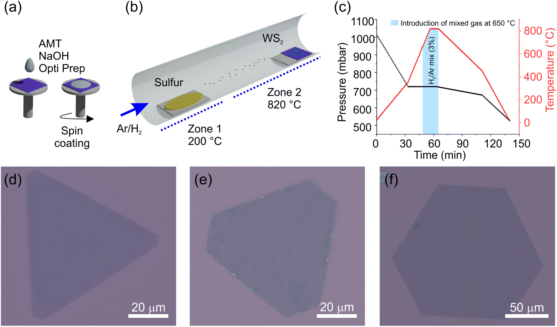 | ||
| Fig. 1 Schematic representation of the LiP-CVD growth process; (a) sample preparation with ammonium metatungstanate (AMT); (b) graphical representation of the reactor; (c) temperature and pressure ramps during the growth. Bright-field optical images of (d) cut-edge (CE), (e) truncated triangles (TT), (f) hexagonal (HX) shaped CVD grown monolayer WS2. | ||
We mapped crystals of each shape by means of Raman spectroscopy, looking at the two most intense Raman active modes of WS2: the out of plane A1g and the in plane E2g. In Fig. 2 we report the result of this mapping by showing the spatial distribution of the Raman-shift difference between the maxima of the A1g and E2g peaks (a–c) per shape. The reason for this choice is twofold: on the one hand it provides an immediate assessment of the single-layer nature of the crystals, as it was found to be a more reliable figure with respect to the intensity ratio.42,46–50 On the other hand, the spatial mapping clearly distinguishes between two regions within each shape. In panel (d) we show the plot of the peak position difference A1g–E2g for each region and shape. The values are calculated as the average of the number of pixels included in the colored squares in panels (a–c) on three different positions of the flake. In panel (e) and (f), we show the positions of the A1g and E2g peaks, evaluated in the same way (cf. Fig. S1 and S2 in the ESI† for the Raman spectra). It appears that the frequency difference between the peaks is mostly driven by the position of the out-of-plane mode A1g, which is known to be sensitive to the doping level of the system.51–53 In particular, A1g was observed to be highly sensitive to the presence of sulfur vacancy (VS) defects.50,53–55 The in-plane E2g mode shows instead a shape-dependent dispersion, indicating a different amount of strain transferred on the crystal lattice, depending on the growth conditions.56–58
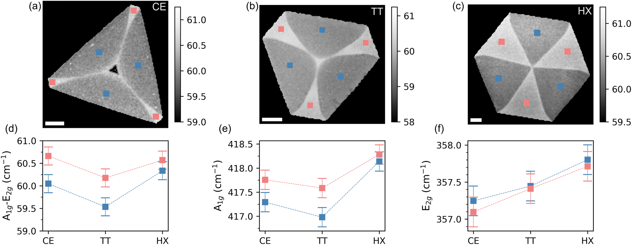 | ||
| Fig. 2 2D frequency difference maps of (a) cut-edge, (b) truncated, (c) hexagonal shaped monolayer WS2 measured by Raman spectroscopy. Scalebar 15 μm. (d) Comparisons of frequency difference in the alternating domains of each WS2. (e) A1g position over each domain and shape (f) E2g position over each domain and shape. | ||
The findings from the Raman scattering measurements are confirmed by the results obtained from the PL analysis, which is reported in Fig. 3. The intensity distribution of the PL signal mirrors the A1g position from Fig. 2, defining bright (high PL intensity) and dark (low PL intensity) regions on every crystal shape. This marked difference in PL intensity between the two domains in WS2 has been discussed in the literature and the defects responsible for non-radiative recombination in monolayer hexagonal WS2 were indicated as complex vacancies involving both tungsten (W) and sulfur (S) atoms, referred to as WSx-vacancy defects.59 These defects create localized states that trap excitons, leading to non-radiative recombination processes. The intensity of the color maps in panels (a) to (c) are logarithmic, to better discriminate between the substrate and the dark domains. PL values averaged on the three bright (dark) regions, are reported in panel (d). The reversed contrast between the two maps is consistent with the results from the work of Lee et al.,50 where a redshift of the A1g mode (cf.Fig. 2(e)) is related to the presence of VS. At the same time, VS domains are observed to favor radiative relaxation channels of optically excited quasiparticles in WS2.60–63 Conversely, the dark regions are assigned to tungsten-deficient areas (VW), in agreement with the results from the research of An et al.38 A comparison between the PL emission of dark and bright domains is provided in panels (e) and (f) of Fig. 3, where we see the VS domains emitting light about ten times more than VW domains. In addition, we see that while TT and HX crystals exhibit very similar line shapes, CE crystals have a different peak shape, indicating a substantially different quasiparticle relaxation dynamics. To better highlight these differences, we report the PL spectra with normalized intensities in Fig. S3 in the ESI.† The PL spectra reveal the importance of the high-defect density in this kind of crystals. The spectra are fitted, after subtracting a linear background, with three Voigt functions accounting for defect-bound exciton (XD), trionic peak (X−) and neutral exciton (X0)64 (cf. Fig. S4†). The trionic peak, which we locate at (1.95 ± 0.01) eV (or 633 ± 3 nm) for the bright and (1.97 ± 0.01) eV (or 626 ± 3 nm) for the dark domain, is dominant with respect to the radiative processes forming the signal of the neutral exciton, located at (2.00 ± 0.01) eV (or 617 ± 3 nm) and (2.02 ± 0.01) eV (or 611 ± 3 nm) for the bright and dark domains, respectively. The observed average ∼15 meV blueshift in the case of the CE crystals implies the fact that the crystalline quality is higher if compared with the other shapes. The lower defect density is also confirmed by looking at the ratio between the X0 and X− peaks59,65 (cf.Fig. 3), visibly higher than for the TT and HX shapes. The lowest binding energy peak is ascribed to defect bound excitons as reported in ref. 64.
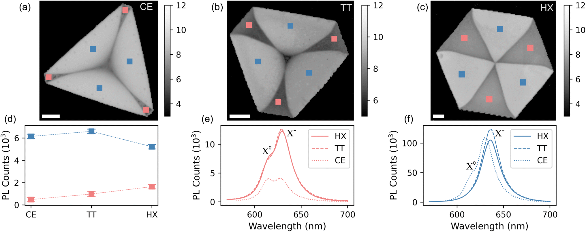 | ||
| Fig. 3 PL log intensity maps of cut-edged (a), truncated (b), hexagonal (c) monolayer WS2. Scalebar 15 μm. (d) Average PL intensity over each domain and shape. (e) Dark domain PL spectra per each shape. (f) Bright domain PL spectra per each shape. | ||
In order to have a more quantitative and chemically sensitive measure of the nature of the defect sites, we carried out selected-area XPS measurements. Because of instrumental limitations, we decided to do this only on HX crystals, as they provide the largest share of bright and dark domains and are therefore easier to identify. The core level spectra in Fig. 4(a) and (b) were extracted from the X-ray photoemission electron microscopy (XPEEM) volume, of which we display the integrated-intensity image in panel (c). The field of view (FOV) of the area is 76.6 μm and the spectra are averaged over areas of 16 × 16 μm2, gathered from the bright (blue circles) and dark (light red) areas, where the nomenclature is referenced to the PL data reported in Fig. 3. In the visualized spectra, a linear background has been first subtracted and the intensity was normalized to 1. Both S 2p and W 4f core levels are composed of two-component doublets, where the second, low binding energy component (WII and SII for W 4f and S 2p respectively) is a measure of the out-of-coordination atoms in the two regions, i.e. an estimate of the defect concentration. The more pronounced peak (SI/WI) corresponds to the pristine crystal, while the less pronounced peak (SII/WII) is linked to S and W atoms exhibiting distinct coordination. Specifically, when analyzing the S core level, insights into the missing W atoms can be gleaned from observing SII, since it affects the chemical shift of neighboring S atoms, and conversely, examining WII provides information about the surrounding S atoms. We extract the relative area of the components in each region and report our findings in Table 1.
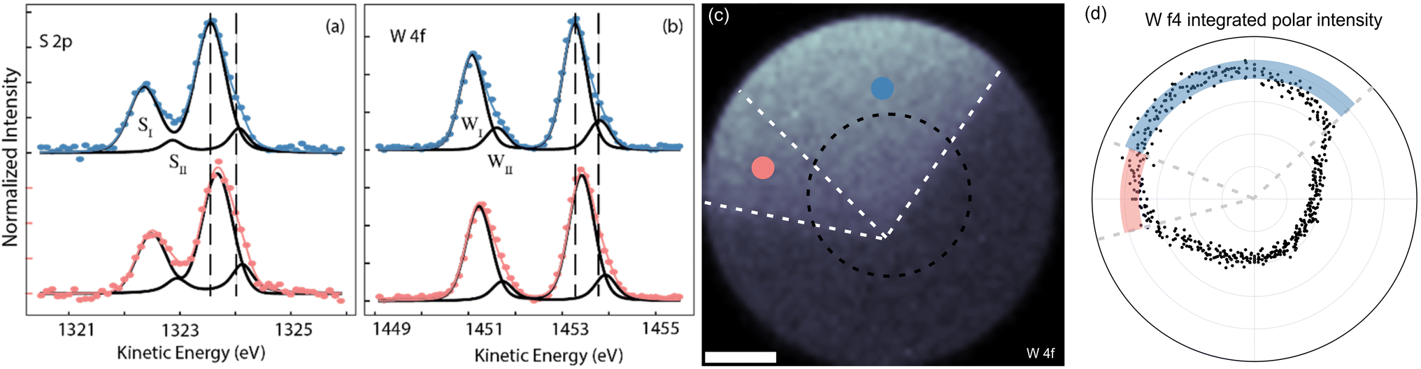 | ||
| Fig. 4 XPS spectra of (a) S 2p and (b) W 4f core levels recorded on the bright (blue) and dark (red) domains. Dots indicate the measured data while continuous lines indicate the fits. Vertical dashed lines have been added to guide the eyes and appreciate the shifts. (c) Spatial XPEEM map of the W 4f integrated intensity. (d) Polar trace of the W 4f integrated intensity, taken along the dashed circle in panel (c). The polar coordinate is the angle, while the radial coordinate is the intensity. Black dots are measured integrated intensity. The two colored bands highlight the intensity in the dark and bright domains. | ||
| Component | Bright | Dark | Delta |
|---|---|---|---|
| SII | (13.5 ± 2.5)% | (18.5 ± 2.5)% | (25.5 ± 1.5)% |
| WII | (17.5 ± 2.5)% | (16.5 ± 2.5)% | (6.5 ± 1.5)% |
These values could be translated into a defect density by considering the atomic density (per layer) of WS2, which is 1.16 × 1015 cm−2. However, as the missing atoms do not contribute to the photoemission signal, the integral of each peak does not consider the vacancy defects, therefore providing an underestimation of the total number of photoemitters (i.e. atoms). This consideration implies that from the XPS data, we can only provide an upper limit for the defect density in the low 1014 cm−2 range. We note that the SII component is more intense in the dark region, while WII has a much lower variation across the two regions. From this observation, we infer that the two regions have concentration of sulfur vacancy defects, differing for just about 6%. Conversely, the relative area of the SII component differs by about 25% between the two domains. Such a difference in tungsten vacancy between the dark and bright domains is in line with what was reported in literature.37,38,55,66 This higher incidence of VW in the dark regions, induces a stronger defective component (SII) in the S 2p spectrum. We observe two different chemical shifts associated with XPS. The first is the shift between the main component, coming from stochiometric WS2, and the defect-related component. The second is the shift between the lines coming from dark and bright domains. The latter is due to a difference in dielectric environment, as it changes the electronic screening of the core level by altering the relaxation energy of the photohole.67–69 For both S 2p and W 4f, these shifts are (400 ± 50) meV and (100 ± 25) meV, respectively. The lower kinetic energy (higher binding energy) of the core level spectra coming from the bright domains, indicate that those are affected by a lower electronic screening, i.e. their electronic states are all shifted towards higher binding energies.37,54,63,70
The XPS data analysis therefore suggests that the variation in dielectric environment is due to a difference in the concentration of VW defects in the mid-high 1013 cm−2 range, which generates a charge unbalance between the domains of the crystal. In Fig. 4(d) we show the polar plot of the XPEEM integrated intensity of the W 4f core level, measured along the black dashed circle in panel (c). To guide the reader, we have superimposed the boundaries of the WS2 crystal also on the plot of panel (d). The line bisecting the domains forms an angle smaller than 60° with the edge of the VW side, as the domain has a funnel-like shape, as visible in Fig. 3(c). As the center of the line profile is different from the vertex of the hexagon, so are the boundaries of the flake in polar coordinates. The thick red and blue bands highlight the distribution of points in the dark and bright domains, respectively. Excluding border effects and noise, the signal from the dark domains is about (7 ± 2)% lower than the signal (i.e. the integrated W 4f intensity) from the bright domains, confirming the difference in intensity to originate from the WII component. The polar plot of Fig. 4(d) also shows that the intensity of W 4f does not go to zero outside of the flake. This is because, outside the flake there are still traces of unreacted precursors containing W and S.
The consequences of this charge unbalance on the optical and electronic properties of WS2 are well visible also by means of KPFM. In Fig. 5(a–c) we show micrographs of the surface potential, recorded on the bright and dark domains for each shape. The VS (bright) domains appear to have a higher surface potential, a quantity which we can directly map into the electron affinity of WS2 and conclude that the Fermi level (EF) in the dark domains is about 70 meV closer to the valence band maximum (VBM) then for the VS domains,71 confirming what was inferred from the XPS data. The difference in surface potential value appears to increase depending on the shape of the crystal63 (Fig. 5(d)). This behavior is consistent with the results obtained via Raman spectroscopy and PL, indicating a lower defect density for the CE and TT shapes with respect to the hexagonal crystals. In a previous publication, KPFM was used in conjunction with transmission electron microscopy (TEM) and theoretical simulations, to correlate the measured surface potential to the types of defects in the crystal by means of.72 The qualitative conclusion of that work is that a higher work function is expected for the domains containing defects of W-vacancy type and this is as well what we also find, being the Fermi level of the dark domains, deeper than the one of the bright domains.
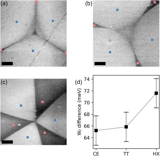 | ||
| Fig. 5 KPFM maps measured in the central region of each shape. (a) CE, (b) TT and (c) HX flake. Scale bar is 5 μm. (d) Plot indicating the work function difference between bright and dark domains as extracted from KPFM measurements for each shape. | ||
In order to gain insight into the electronic properties of the valence band of the system, we performed μARPES (see Methods), by means of which we could map the electron dispersion on the two domains and display it in Fig. 6. Panels (a) and (b) show the band structure of bright and dark domains, respectively. The reference (zero) for the energy scale has been chosen to be the Fermi level. Noticeably, the WS2 spin–orbit splitting of the valence bands in K is not visible in our sample, as shown in panel (c), where we display the energy distribution curves (EDCs) extracted at the K point of the bands recorded on each domain. There are several reasons for this: we are dealing with crystals which have a non-negligible content of defects; for the NanoESCA measurements, the flakes have been transferred onto an Au film (cf. Methods) which was evaporated via physical vapor deposition (PVD), and which therefore retains the intrinsic roughness of a metal PVD film. Considering how ARPES is sensitive to surface irregularities, even a nm of roughness can visibly broaden the signal.73 In addition, the transfer process leaves polymeric residuals on the surface, which increase even further the scattering of the photoemitted carriers. Defective areas have been observed to exhibit a full width at half maximum (FWHM) of 900 meV in nanoARPES.63 Since locating the position of the low-energy spin band is not straightforward by fitting the intensity with two components, we instead estimate the position of the center of the mean value first by subtracting the contribution to the signal from the secondary electrons (SES) and then extracting 〈E〉 = sum(E × I)/sum(I). The outcome of such a procedure is shown in panel (d), where we see that the two VBM are found (65 ± 10) meV apart, with the bands of the bright domains deeper in binding energy. This result is quantitatively consistent with the values measured by KPFM, as well as with the work function data extracted from the NanoESCA (cf. Fig. S4 in the ESI†).
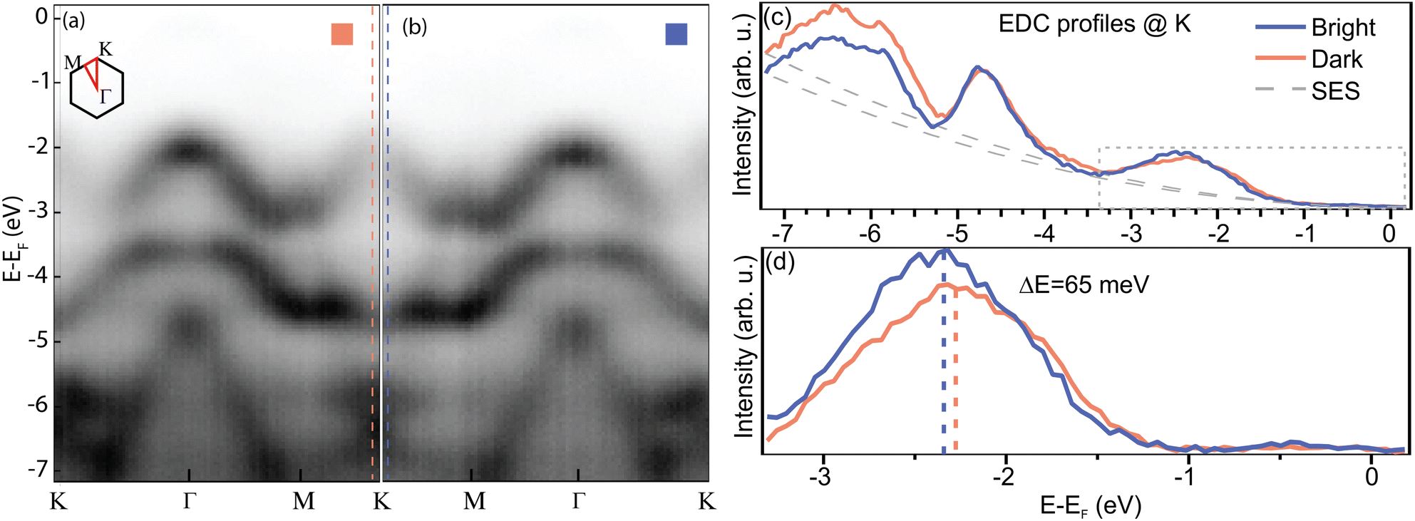 | ||
| Fig. 6 μARPES spectra comparing the band structure recorded on (a) dark and (b) bright domains. (c) Difference between the spectral intensity in (a) and (b), highlighting the energy shift between the two. (d) Zoom-in of the region framed in panel (c), highlighting the energy difference between the VBM in the two domains. | ||
The type and density of defects have a relevant impact on the quasiparticle dynamics of the system. Li and Carter74 reported on exciton recombination dynamics in the presence of various defective species in WSe2. They demonstrated how the W vacancies act as carrier traps. This behavior has a two-fold effect: it hinders radiative recombination paths, promoting a competing non-radiative electron–hole annihilation,70 but it also mitigates the effect of an external field. When a gate is applied, the presence of charge carrier traps, prevents the formation of trions, i.e. charged excitons. At the same time, trapping extra carriers screens the effect of the gate on the dielectric environment, leaving the neutral exciton X0 largely unaffected by the application of a bias voltage.14 To investigate that, we carried out gate-dependent PL experiments on TT crystals, reported in Fig. 7. Panel (a) and (b) display the normalized PL emission for bright and dark regions respectively. The stark contrast in intensity modulation as a function of the applied field is clear. However, we can better quantify this behavior by fitting the curves with three components64,75 as specified above, describing the defect bound exciton, the trion and the neutral exciton from lower to higher energy respectively. The plots from panels (a) and (b) are reported deconvolved into three components in panels (c) and (d) for the bright and dark domains, respectively. Tracking the intensity of the trion peak (Fig. 7(e)), we see how it changes by almost 15% of the total intensity as a function of the gate for the bright region. Conversely, the trion in the dark region changes its intensity by a mere 5%. These observations agree well with the model of VW acting as carriers trap described above. Over the measured TT crystals, we observe a of zero-bias energy difference in the neutral exciton emission between the dark and bright domains of about 15 meV. This suggests a variation in the optical band gap between two domains. The amplitude of the optical gap is given by the quasiparticle bandgap minus the binding energy of the exciton, i.e. Eo = Eg − Eb. Assuming the energy shift in the valence bands as rigid,76 implies the band dispersion to remain unchanged (i.e. no band renormalization occurring), and the difference in Eg between the two domains is therefore twice the measured difference in the position of the valence band maximum, that is 130 meV. From these relations, we find that the disparity in the binding energy of the X0 between bright and dark domains is ΔEb = ΔEg − ΔEo = 2ΔEVBM − ΔEo = 115 meV. In literature, the binding energy of the neutral exciton is reported to be anywhere between 320 meV77 and 710 meV.78 The relative difference we find in our work could therefore represent a discrepancy between 16% and 35% from one domain to the other.
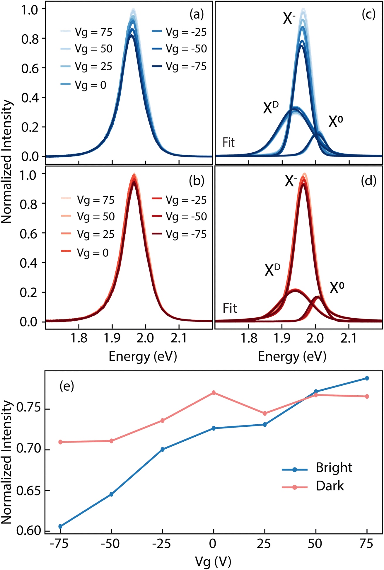 | ||
| Fig. 7 Gate-dependent PL spectra measured on (a) bright and (b) dark domains. Fitting curve representing neutral (X0), charged (X−) and defect-bound (XD) excitons for bright (c) and dark domains (d). (e) Dispersion of the trion (X−) emission intensity as a function of the gate voltage. | ||
Conclusions
In this work we have successfully synthetized LiP-CVD monolayer tungsten disulfide in different shapes, by controlling the Ar background pressure in the reactor. The resulting crystals have been probed via numerous techniques to unravel their structural, optical and electronic properties. We have found that the defects that are formed during the growth are point-defects represented by sulfur and tungsten vacancies, distributed following the symmetry of the crystal and having an extent which is shape-dependent. The shape of the crystal determines also the amount of strain across the crystal, which is mapped by the shift of the E2g Raman mode, as well as the A1g position provides a way of mapping the carrier distribution. Further independent measurements via μXPS, KPFM and μARPES, reveal that the domains which are bright in PL contain a VS concentration of the order of several in 1013 cm−2, corresponding to an n-type doping of (75 ± 25) meV with respect to the VW (dark) domains. Such a defect density on each domain implies that the radiative processes are dominated by the relaxation of the charged exciton X−. In the VS domains, the radiative channel of the X0 decay is not hindered and therefore still bright in the PL spectrum. Despite the fact that we could not access a precise determination of the quasiparticle bandgap and hence to the dielectric constant on each domain, we can still provide a route for engineering lateral, atomically sharp crystal domains, with heterogeneous dielectric environments. Deepening the comprehension of the mechanisms by which defects are generated will lead to their control and tailoring within the TMD crystal lattice, which represents a crucial step towards their exploitation of advanced technologies for quantum information.Methods
Synthesis and semidry transfer of monolayer WS2
Monolayer WS2 was grown via liquid-phase chemical vapor deposition (LiP-CVD) similarly to what was reported by Kim et al.35 In this method, the liquid precursors are mixed at a determined ratio and spun onto the target substrate. We dissolved 150 mg of ammonium metatungstate (AMT, Sigma-Aldrich) as tungsten source in deionized (DI) water (solution A) and 100 mg of NaOH pellet (Sigma-Aldrich) as promoter in 40 ml DI water (solution B) to prepare the mother solutions. Opti Prep (Sigma-Aldrich), a density gradient medium, was used as solution C to improve the spin casting process. Solution A, B and C were mixed in the ratio of 1![[thin space (1/6-em)]](https://www.rsc.org/images/entities/char_2009.gif) :4:2 before spinning. As in the work of Pace et al.,79 after cleaning via sonication in acetone and isopropanol, the SiO2/Si substrates were treated with oxygen plasma to improve the homogeneity of the distribution of the precursor and thus the growth performance. The mixture of precursors was dropped on the SiO2/Si substrate and the substrate was spin-coated at 4000 rpm for 1 min, as schematized in Fig. 1(a). The sulfur and the spin-coated sample were placed in a Lenton hot-wall horizontal CVD reactor as displayed in Fig. 1(b). The different shapes, cut-edges triangles, truncated triangles and hexagons, were obtained by setting the background pressure at different levels: 820, 780 and 720 mbar, respectively, while maintaining the temperature at 820 °C, the dwell time at 7 min and the Ar flux at 30 sccm. At 650 °C, we introduced an H2/Ar (3%) mixture gas into the system, followed by a switch back to pure Ar at the end of the dwell time. By decreasing the pressure, we reduced the amount of sulfur reacting with the W precursor, obtaining a result similar to the one reported in ref. 36. The schematic of the main steps of the growth process is shown in Fig. 1(c).
:4:2 before spinning. As in the work of Pace et al.,79 after cleaning via sonication in acetone and isopropanol, the SiO2/Si substrates were treated with oxygen plasma to improve the homogeneity of the distribution of the precursor and thus the growth performance. The mixture of precursors was dropped on the SiO2/Si substrate and the substrate was spin-coated at 4000 rpm for 1 min, as schematized in Fig. 1(a). The sulfur and the spin-coated sample were placed in a Lenton hot-wall horizontal CVD reactor as displayed in Fig. 1(b). The different shapes, cut-edges triangles, truncated triangles and hexagons, were obtained by setting the background pressure at different levels: 820, 780 and 720 mbar, respectively, while maintaining the temperature at 820 °C, the dwell time at 7 min and the Ar flux at 30 sccm. At 650 °C, we introduced an H2/Ar (3%) mixture gas into the system, followed by a switch back to pure Ar at the end of the dwell time. By decreasing the pressure, we reduced the amount of sulfur reacting with the W precursor, obtaining a result similar to the one reported in ref. 36. The schematic of the main steps of the growth process is shown in Fig. 1(c).
When needed the monolayer WS2 was transferred onto the desired substrate via a semidry approach.80–83 In particular, the WS2 substrate was covered with a double-layer of polymethylmethacrylate (PMMA AR-P 679.02, Allresist) and 15% polypropylene carbonate in anisole (PPC, Sigma-Aldrich), which were sequentially spun and baked at 90 °C for 2 min. The sample was then covered with a few-millimeter-thick polydimethylsiloxane (PDMS) frame, and left floating on NaOH 1 M solution at 70 °C, until the membrane was completely detached. After detachment, the floating membrane was fished out and rinsed in DI water for few minutes to remove the NaOH residuals. Finally, the membrane was transferred onto the target substrate, by using a transfer setup and backed at 90 °C for few minutes. The polymeric membrane was then removed via a standard cleaning in acetone and isopropanol, followed by a deep cleaning in a resist remover (AR-600 71) for 3 min.
Characterization techniques
The optical images of monolayer WS2 were collected with a Zeiss Axioscope microscope using a 50× objective lens.Raman spectroscopy and photoluminescence (PL) measurements were performed with a Renishaw InVia Spectrometer. The samples were illuminated with 473 nm laser light, a fluence of 315 μJ μm−2 and the scattered light was dispersed on a CCD detector with 1015 active pixels via a grating with 2400 lines per mm. The single PL spectra were recorded with a fluence of 31.5 mJ μm−2. The same system, equipped with a Linkam cell for electrical measurements, was used to perform gate-dependent PL measurements. The measurement in the Linkam cell has been performed under dry nitrogen atmosphere, at ambient pressure and room temperature. In this case the fluence was 8 mJ μm−2.
Amplitude-modulated Kelvin Probe Force Microscopy (AM-KPFM) was performed using a Bruker Dimension Icon microscope.
Area-selected μXPS and μARPES were recorded in a NanoEsca momentum microscope (Scienta Omicron GmbH and Focus GmbH).73 The photon source were a monochromatized small spot Al Kα source (1486.6 eV, SPECS GmbH) for XPS and a HeI α (21.22 eV) plasma lamp (FOCUS GmbH) for μARPES.
The XPS peaks of S 2p and W 4f were fitted with two symmetric doublets, where the doublet at low kinetic energy indicates the signal coming from WS2 and the doublet at higher kinetic was assigned to defects. The relative ratio between the area of the component with respect to their sum, provides a higher limit value for the concentration of the defects in the probed region. As each defective component represents the atoms out of coordination, with respect to stoichiometric WS2, each defective component (S or W) is an estimation of the vacancies of the other element (W or S).
For the μXPS and ARPES measurements, the monolayer WS2 was transferred via a semidry approach,79,84 onto a SiO2/Si substrate thermally evaporated with 5 nm Cr and 50 nm Au (see Fabrication).
Fabrication
In the gate-dependent PL measurements we used the 285 nm of SiO2 as dielectric and the p-doped silicon substrate as common back-gate. WS2 crystals were transferred onto a pristine SiO2/Si substrate, as described previously. The transfer was required because the growth process led to some holes and defects in the SiO2 (ref. 79) that may limit the use as a dielectric. To have a common ground connection on the crystals, metallic contacts were made via optical lithography. Optical lithography was performed in a laser writer MicroWriter ML3 Pro, with 365 nm light source and spatial resolution of 0.7 μm. Microposit S1813 was used as (positive) photoresist, spun at 6000 rpm for 1 minute and dried for 2 minutes at 110 °C. The photoresist was exposed with a dose of 150 mJ cm−2 and developed in MF-319 for 30 seconds. The metallic contacts were then made via thermal metal evaporation of 50 nm Au on top of 5 nm of Ti as adhesion layer. The lift-off and the cleaning of the device from the polymeric residual, was made by 50 minutes in acetone, 3 minutes in isopropanol and drying the sample via nitrogen-gas flux.Conflicts of interest
There are no conflicts to declare.Acknowledgements
This work is supported by the European Union's Horizon 2020 research and innovation program – GA 881603 and the Scientific and Technological Research Council of Turkey (TUBITAK). We acknowledge the PNRR MUR project PE0000023-NQSTI.References
- M.-L. Tsai, S.-H. Su, J.-K. Chang, D.-S. Tsai, C.-H. Chen, C.-I. Wu, L.-J. Li, L.-J. Chen and J.-H. He, ACS Nano, 2014, 8, 8317–8322 CrossRef CAS PubMed.
- D. Kufer and G. Konstantatos, Nano Lett., 2015, 15, 7307–7313 CrossRef CAS PubMed.
- H. Tan, Y. Fan, Y. Zhou, Q. Chen, W. Xu and J. H. Warner, ACS Nano, 2016, 10, 7866–7873 CrossRef CAS PubMed.
- Y. Xue, Y. Zhang, Y. Liu, H. Liu, J. Song, J. Sophia, J. Liu, Z. Xu, Q. Xu, Z. Wang, J. Zheng, Y. Liu, S. Li and Q. Bao, ACS Nano, 2016, 10, 573–580 CrossRef CAS PubMed.
- C. Lan, Z. Zhou, Z. Zhou, C. Li, L. Shu, L. Shen, D. Li, R. Dong, S. P. Yip and J. C. Ho, Nano Res., 2018, 11, 3371–3384 CrossRef CAS.
- T. Mueller and E. Malic, npj 2D Mater. Appl., 2018, 2, 1–12 CrossRef CAS.
- W. Zhao, Z. Ghorannevis, L. Chu, M. Toh, C. Kloc, P. H. Tan and G. Eda, ACS Nano, 2013, 7, 791–797 CrossRef CAS PubMed.
- H.-C. Kim, H. Kim, J.-U. Lee, H.-B. Lee, D.-H. Choi, J.-H. Lee, W. H. Lee, S. H. Jhang, B. H. Park, H. Cheong, S.-W. Lee and H.-J. Chung, ACS Nano, 2015, 9, 6854–6860 CrossRef CAS PubMed.
- S. Forti, A. Rossi, H. Büch, T. Cavallucci, F. Bisio, A. Sala, T. O. Menteş, A. Locatelli, M. Magnozzi, M. Canepa, K. Müller, S. Link, U. Starke, V. Tozzini and C. Coletti, Nanoscale, 2017, 9, 16412–16419 RSC.
- A. Rossi, H. Büch, C. Di Rienzo, V. Miseikis, D. Convertino, A. Al-Temimy, V. Voliani, M. Gemmi, V. Piazza and C. Coletti, 2D Mater., 2016, 3, 031013 CrossRef.
- J. Wang, H. Li, Y. Ma, M. Zhao, W. Liu, B. Wang, S. Wu, X. Liu, L. Shi, T. Jiang and J. Zi, Light: Sci. Appl., 2020, 9, 148 CrossRef PubMed.
- G. Plechinger, P. Nagler, J. Kraus, N. Paradiso, C. Strunk, C. Schüller and T. Korn, Phys. Status Solidi RRL, 2015, 9, 457–461 CrossRef CAS.
- A. Chernikov, A. M. Van Der Zande, H. M. Hill, A. F. Rigosi, A. Velauthapillai, J. Hone and T. F. Heinz, Phys. Rev. Lett., 2015, 115, 1–6 CrossRef PubMed.
- B. Liu, W. Zhao, Z. Ding, I. Verzhbitskiy, L. Li, J. Lu, J. Chen, G. Eda and K. P. Loh, Adv. Mater., 2016, 28, 6457–6464 CrossRef CAS PubMed.
- J. Shang, X. Shen, C. Cong, N. Peimyoo, B. Cao, M. Eginligil and T. Yu, ACS Nano, 2015, 9, 647–655 CrossRef CAS PubMed.
- M. Paur, A. J. Molina-Mendoza, R. Bratschitsch, K. Watanabe, T. Taniguchi and T. Mueller, Nat. Commun., 2019, 10, 1–7 CrossRef CAS PubMed.
- C. Cong, J. Shang, Y. Wang and T. Yu, Adv. Opt. Mater., 2018, 6, 1700767 CrossRef.
- M. Magnozzi, T. Pflug, M. Ferrera, S. Pace, L. Ramó, M. Olbrich, P. Canepa, H. Ağircan, A. Horn, S. Forti, O. Cavalleri, C. Coletti, F. Bisio and M. Canepa, J. Phys. Chem. C, 2021, 125, 16059–16065 CrossRef CAS PubMed.
- S. Feng, C. Cong, S. Konabe, J. Zhang, J. Shang, Y. Chen, C. Zou, B. Cao, L. Wu, N. Peimyoo, B. Zhang and T. Yu, Small, 2019, 15, 1–7 CrossRef PubMed.
- A. W. Cummings, J. H. Garcia, J. Fabian and S. Roche, Phys. Rev. Lett., 2017, 119, 206601 CrossRef PubMed.
- Y. Xue, Y. Zhang, Y. Liu, H. Liu, J. Song, J. Sophia, J. Liu, Z. Xu, Q. Xu, Z. Wang, J. Zheng, Y. Liu, S. Li and Q. Bao, ACS Nano, 2016, 10, 573–580 CrossRef CAS PubMed.
- N. Huo and G. Konstantatos, Adv. Mater., 2018, 30, 1–27 CrossRef PubMed.
- W. Gao, S. Zhang, F. Zhang, P. Wen, L. Zhang, Y. Sun, H. Chen, Z. Zheng, M. Yang, D. Luo, N. Huo and J. Li, Adv. Electron. Mater., 2021, 7, 1–7 Search PubMed.
- P. Cheng, K. Sun and Y. H. Hu, Nano Lett., 2016, 16, 572–576 CrossRef CAS PubMed.
- R. Ge, X. Wu, L. Liang, S. M. Hus, Y. Gu, E. Okogbue, H. Chou, J. Shi, Y. Zhang, S. K. Banerjee, Y. Jung, J. C. Lee and D. Akinwande, Adv. Mater., 2021, 33, 1–9 Search PubMed.
- R. Ge, X. Wu, M. Kim, J. Shi, S. Sonde, L. Tao, Y. Zhang, J. C. Lee and D. Akinwande, Nano Lett., 2018, 18, 434–441 CrossRef CAS PubMed.
- B. Schuler, J. H. Lee, C. Kastl, K. A. Cochrane, C. T. Chen, S. Refaely-Abramson, S. Yuan, E. Van Veen, R. Roldán, N. J. Borys, R. J. Koch, S. Aloni, A. M. Schwartzberg, D. F. Ogletree, J. B. Neaton and A. Weber-Bargioni, ACS Nano, 2019, 13, 10520–10534 CrossRef CAS PubMed.
- A. Rossi, J. C. Thomas, J. T. Küchle, E. Barré, Z. Yu, D. Zhou, S. Kumari, H.-Z. Tsai, E. Wong, C. Jozwiak, A. Bostwick, J. A. Robinson, M. Terrones, A. Raja, A. Schwartzberg, D. F. Ogletree, J. B. Neaton, M. F. Crommie, F. Allegretti, W. Auwärter, E. Rotenberg and A. Weber-Bargioni, arXiv, 2023, preprint, arXiv:2301.02721v2, DOI:10.48550/arXiv.2301.02721.
- A. Singh and A. K. Singh, Phys. Rev. Mater., 2021, 5, 2–10 Search PubMed.
- B. Schuler, K. A. Cochrane, C. Kastl, E. S. Barnard, E. Wong, N. J. Borys, A. M. Schwartzberg, D. F. Ogletree, F. J. G. de Abajo and A. Weber-Bargioni, Sci. Adv., 2020, 6, 1–8 Search PubMed.
- X. Xin, Y. Zhang, J. Chen, M.-L. Chen, W. Xin, M. Ding, Y. Bao, W. Liu, H. Xu and Y. Liu, Mater. Horiz., 2022, 9, 2416–2424 RSC.
- J. Y. Tsai, J. Pan, H. Lin, A. Bansil and Q. Yan, Nat. Commun., 2022, 13, 1–9 Search PubMed.
- J. A. Robinson and B. Schuler, Appl. Phys. Lett., 2021, 119, 140501 CrossRef CAS.
- S. J. Yun, S. H. Chae, H. Kim, J. C. Park, J.-H. Park, G. H. Han, J. S. Lee, S. M. Kim, H. M. Oh, J. Seok, M. S. Jeong, K. K. Kim and Y. H. Lee, ACS Nano, 2015, 9, 5510–5519 CrossRef CAS PubMed.
- H. Kim, G. H. Han, S. J. Yun, J. Zhao, D. H. Keum, H. Y. Jeong, T. H. Ly, Y. Jin, J.-H. Park, B. H. Moon, S.-W. Kim and Y. H. Lee, Nanotechnology, 2017, 28, 36LT01 CrossRef PubMed.
- A. Zafar, Z. Zafar, W. Zhao, J. Jiang, Y. Zhang, Y. Chen, J. Lu and Z. Ni, Adv. Funct. Mater., 2019, 29, 1–8 CrossRef.
- H. Y. Jeong, Y. Jin, S. J. Yun, J. Zhao, J. Baik, D. H. Keum, H. S. Lee and Y. H. Lee, Adv. Mater., 2017, 29, 1–6 Search PubMed.
- G. H. An, S. J. Yun, Y. H. Lee and H. S. Lee, Small, 2020, 16, 1–9 CrossRef PubMed.
- C. Lee, B. G. Jeong, S. H. Kim, D. H. Kim, S. J. Yun, W. Choi, S. J. An, D. Lee, Y. M. Kim, K. K. Kim, S. M. Lee and M. S. Jeong, npj 2D Mater. Appl., 2022, 6, 1–9 CrossRef CAS.
- J. Kim, G. H. An, S. Bang, D. G. Park, D. Kim, S. Jin, M. J. Kim, H. S. Lee and J. W. Lee, Appl. Surf. Sci., 2022, 604, 154600 CrossRef CAS.
- S. Li, S. Wang, D.-M. Tang, W. Zhao, H. Xu, L. Chu, Y. Bando, D. Golberg and G. Eda, Appl. Mater. Today, 2015, 1, 60–66 CrossRef.
- M. S. Kim, S. J. Yun, Y. Lee, C. Seo, G. H. Han, K. K. Kim, Y. H. Lee and J. Kim, ACS Nano, 2016, 10, 2399–2405 CrossRef CAS PubMed.
- T. H. Choudhury, H. Simchi, R. Boichot, M. Chubarov, S. E. Mohney and J. M. Redwing, Cryst. Growth Des., 2018, 18, 4357–4364 CrossRef CAS.
- Y. Zhang, Y. Zhang, Q. Ji, J. Ju, H. Yuan, J. Shi, T. Gao, D. Ma, M. Liu, Y. Chen, X. Song, H. Y. Hwang, Y. Cui and Z. Liu, ACS Nano, 2013, 7, 8963–8971 CrossRef CAS PubMed.
- J. Chen, B. Liu, Y. Liu, W. Tang, C. T. Nai, L. Li, J. Zheng, L. Gao, Y. Zheng, H. S. Shin, H. Y. Jeong and K. P. Loh, Adv. Mater., 2015, 27, 6722–6727 CrossRef CAS PubMed.
- S.-L. Li, H. Miyazaki, H. Song, H. Kuramochi, S. Nakaharai and K. Tsukagoshi, ACS Nano, 2012, 6, 7381–7388 CrossRef PubMed.
- C. Lee, H. Yan, L. E. Brus, T. F. Heinz, J. Hone and S. Ryu, ACS Nano, 2010, 4, 2695–2700 CrossRef CAS PubMed.
- A. Berkdemir, H. R. Gutiérrez, A. R. Botello-Méndez, N. Perea-López, A. L. Elías, C.-I. Chia, B. Wang, V. H. Crespi, F. López-Urías, J.-C. Charlier, H. Terrones and M. Terrones, Sci. Rep., 2013, 3, 1755 CrossRef.
- W. Zhao, Z. Ghorannevis, K. K. Amara, J. R. Pang, M. Toh, X. Zhang, C. Kloc, P. H. Tan and G. Eda, Nanoscale, 2013, 5, 9677 RSC.
- C. Lee, B. G. Jeong, S. J. Yun, Y. H. Lee, S. M. Lee and M. S. Jeong, ACS Nano, 2018, 12, 9982–9990 CrossRef CAS PubMed.
- Y. Jin, D. H. Keum, S. An, J. Kim, H. S. Lee and Y. H. Lee, Adv. Mater., 2015, 27, 5534–5540 CrossRef CAS PubMed.
- M. W. Iqbal, K. Shahzad, G. Hussain, M. K. Arshad, R. Akbar, S. Azam, S. Aftab, T. Alharbi and A. Majid, Mater. Res. Express, 2019, 6, 115909 CrossRef CAS.
- J. Kim, G. H. An, S. Bang, D. G. Park, D. Kim, S. Jin, M. J. Kim, H. S. Lee and J. W. Lee, Appl. Surf. Sci., 2022, 604, 154600 CrossRef CAS.
- S. Salehi and A. Saffarzadeh, Surf. Sci., 2016, 651, 215–221 CrossRef CAS.
- Y. Lin, S. Li, H. Komsa, L. Chang, A. V. Krasheninnikov, G. Eda and K. Suenaga, Adv. Funct. Mater., 2018, 28, 1–8 Search PubMed.
- Y. Y. Hui, X. Liu, W. Jie, N. Y. Chan, J. Hao, Y. Te Hsu, L. J. Li, W. Guo and S. P. Lau, ACS Nano, 2013, 7, 7126–7131 CrossRef CAS PubMed.
- F. Wang, I. A. Kinloch, D. Wolverson, R. Tenne, A. Zak, E. O'Connell, U. Bangert and R. J. Young, 2D Mater., 2016, 4, 015007 CrossRef.
- P. Kumar, B. Singh, P. Kumar and V. Balakrishnan, J. Mater. Chem. C, 2018, 6, 11407–11415 RSC.
- K. Wu, H. Zhong, Q. Guo, J. Tang, Z. Yang, L. Qian, S. Yuan, S. Zhang and H. Xu, Adv. Opt. Mater., 2022, 10, 1–8 RSC.
- Z. Wu, W. Zhao, J. Jiang, T. Zheng, Y. You, J. Lu and Z. Ni, J. Phys. Chem. C, 2017, 121, 12294–12299 CrossRef CAS.
- L. Gao, Q. Liao, X. Zhang, X. Liu, L. Gu, B. Liu, J. Du, Y. Ou, J. Xiao, Z. Kang, Z. Zhang and Y. Zhang, Adv. Mater., 2020, 32, 1–10 Search PubMed.
- J. Jiang, C. Ling, T. Xu, W. Wang, X. Niu, A. Zafar, Z. Yan, X. Wang, Y. You, L. Sun, J. Lu, J. Wang and Z. Ni, Adv. Mater., 2018, 30, 1–6 Search PubMed.
- C. Kastl, R. J. Koch, C. T. Chen, J. Eichhorn, S. Ulstrup, A. Bostwick, C. Jozwiak, T. R. Kuykendall, N. J. Borys, F. M. Toma, S. Aloni, A. Weber-Bargioni, E. Rotenberg and A. M. Schwartzberg, ACS Nano, 2019, 13, 8b06574 CrossRef PubMed.
- R. Kesarwani, K. B. Simbulan, T.-D. Huang, Y.-F. Chiang, N.-C. Yeh, Y.-W. Lan and T.-H. Lu, Sci. Adv., 2022, 8, 1–9 Search PubMed.
- Q. Cui, Z. Luo, Q. Cui, W. Zhu, H. Shou, C. Wu, Z. Liu, Y. Lin, P. Zhang, S. Wei, H. Yang, S. Chen, A. Pan and L. Song, Adv. Funct. Mater., 2021, 31, 1–10 Search PubMed.
- B. G. Jeong, C. Lee, S. H. Kim, S. J. Yun, D. H. Kim, J. Lee, D. Lee, K. K. Kim, S. C. Lim and M. S. Jeong, J. Phys. Chem. C, 2022, 126, 7177–7183 CrossRef CAS.
- S. P. Kowalczyk, L. Ley, R. L. Martin, F. R. McFeely and D. A. Shirley, Faraday Discuss. Chem. Soc., 1975, 60, 7–17 RSC.
- F. Bechstedt, R. Enderlein, R. Fellenberg, P. Streubel and A. Meisel, J. Electron Spectrosc. Relat. Phenom., 1983, 31, 131–143 CrossRef CAS.
- J. A. Mejías, V. M. Jiménez, G. Lassaletta, A. Fernández, J. P. Espinós and A. R. González-Elipe, J. Phys. Chem., 1996, 100, 16255–16262 CrossRef.
- W.-H. Lin, W.-S. Tseng, C. M. Went, M. L. Teague, G. R. Rossman, H. A. Atwater and N.-C. Yeh, ACS Nano, 2020, 14, 1350–1359 CrossRef CAS PubMed.
- S. Salehi and A. Saffarzadeh, J. Phys. Chem. Solids, 2018, 121, 172–176 CrossRef CAS.
- X. Wang, J. Dan, Z. Hu, J. F. Leong, Q. Zhang, Z. Qin, S. Li, J. Lu, S. J. Pennycook, W. Sun and C. H. Sow, Chem. Mater., 2019, 31, 7970–7978 CrossRef CAS.
- B. Matta, P. Rosenzweig, O. Bolkenbaas, K. Küster and U. Starke, Phys. Rev. Res., 2022, 4, 023250 CrossRef CAS.
- L. Li and E. A. Carter, J. Am. Chem. Soc., 2019, 141, 10451–10461 CrossRef CAS PubMed.
- R. Kesarwani, K. B. Simbulan, T. De Huang, Y. F. Chiang, N. C. Yeh, Y. W. Lan and T. H. Lu, Sci. Adv., 2022, 8, 1–9 Search PubMed.
- L. Waldecker, A. Raja, M. Rösner, C. Steinke, A. Bostwick, R. J. Koch, C. Jozwiak, T. Taniguchi, K. Watanabe, E. Rotenberg, T. O. Wehling and T. F. Heinz, Phys. Rev. Lett., 2019, 123, 206403 CrossRef CAS PubMed.
- A. Chernikov, T. C. Berkelbach, H. M. Hill, A. Rigosi, Y. Li, B. Aslan, D. R. Reichman, M. S. Hybertsen and T. F. Heinz, Phys. Rev. Lett., 2014, 113, 076802 CrossRef CAS PubMed.
- B. Zhu, X. Chen and X. Cui, Sci. Rep., 2015, 5, 9218 CrossRef PubMed.
- S. Pace, L. Martini, D. Convertino, D. H. Keum, S. Forti, S. Pezzini, F. Fabbri, V. Mišeikis and C. Coletti, ACS Nano, 2021, 15, 4213–4225 CrossRef CAS PubMed.
- S. Conti, L. Pimpolari, G. Calabrese, R. Worsley, S. Majee, D. K. Polyushkin, M. Paur, S. Pace, D. H. Keum, F. Fabbri, G. Iannaccone, M. Macucci, C. Coletti, T. Mueller, C. Casiraghi and G. Fiori, Nat. Commun., 2020, 11, 3566 CrossRef CAS PubMed.
- M. Ferrera, L. Ramò, D. Convertino, G. Orlandini, S. Pace, I. Milekhin, M. Magnozzi, M. Rahaman, D. R. T. Zahn, C. Coletti, M. Canepa and F. Bisio, Chemosensors, 2022, 10, 120 CrossRef CAS.
- E. Peci, M. Magnozzi, L. Ramó, M. Ferrera, D. Convertino, S. Pace, G. Orlandini, A. Sharma, I. Milekhin, G. Salvan, C. Coletti, D. R. T. Zahn, F. Bisio and M. Canepa, Adv. Mater. Interfaces, 2023, 10, 1–7 Search PubMed.
- C. Coletti, M. A. Giambra, V. Miseikis, and M. Romagnoli, Italian PatentApplication No. IT102019000005030, Filed on April 3, 2019, International PatentApplication No. PCT/IB2020/052501, Filed on March 19, 2020 Search PubMed.
- V. Miseikis, F. Bianco, J. David, M. Gemmi, V. Pellegrini, M. Romagnoli and C. Coletti, 2D Mater., 2017, 4, 021004 CrossRef.
Footnote |
| † Electronic supplementary information (ESI) available. See DOI: https://doi.org/10.1039/d4na00125g |
| This journal is © The Royal Society of Chemistry 2024 |