
 Open Access Article
 This Open Access Article is licensed under a Creative Commons Attribution-Non Commercial 3.0 Unported Licence
Nanoscale liquid Al phase formation through beam heating of MgAl2O4 in TEM†
Sung Bo
Lee
 *,
Jun Young
Chae
and
Heung Nam
Han
*,
Jun Young
Chae
and
Heung Nam
Han
Department of Materials Science and Engineering and Research Institute of Advanced Materials, Seoul 08826, Republic of Korea. E-mail: bolee@snu.ac.kr
First published on 29th March 2024
Abstract
In this study, electron-beam irradiation of a MgAl2O4 single-crystalline thin-film specimen in a transmission electron microscope reveals an unexpected formation of nanoscale liquid Al droplets. Despite the comparable melting temperatures of Mg and Al, the resulting liquid phase is predominantly composed of Al. This predominant presence of Al in the liquid phase is attributed to the selective evaporation of Mg, driven by its higher vapor pressure at elevated temperatures. Our observations suggest a correlation between electron-beam irradiation and a subsequent rise in specimen temperature. In particular, the observed melting of Al defies explanation by the widely accepted mechanism that attributes specimen heating to electron-energy loss, given the negligible energy deposited as determined by the collision stopping power. Instead, we suggest that the significant specimen heating is due to Auger excitation, a process known to deposit substantial energy. This contention is supported by a quantitative heat-transfer finite element analysis.
Introduction
Electron-beam damage in transmission electron microscopes (TEMs) manifests itself through a spectrum of mechanisms, encompassing knock-on atomic displacement, sputtering, radiolysis, and electron-beam heating.1,2 Incident electrons engage with nuclei through elastic scattering, causing knock-on atomic displacement and sputtering. Radiolysis and electron-beam heating arise from inelastic electron–electron scattering. Knock-on atomic displacement refers to the movement of atoms induced by electron bombardment, while sputtering involves the ejection of atoms from a solid surface. Radiolysis is the breaking of chemical bonds caused by the transfer of the electron-beam energy.In the realm of electron-beam heating, two energy transfer mechanisms were proposed: direct dissipation of kinetic energy from incident electrons (electron-energy loss)1–3 and generation of excited electronic states,4 potentially through Auger excitation.5 While many studies have shown the importance of beam heating in understanding nanoparticle dynamics and melting,6–10 the lack of comprehensive quantitative analysis leaves the relative dominance of each mechanism unclear. This uncertainty hinders accurate interpretation of observed behavior and necessitates further investigation into the specific heat-transfer processes at the nanoscale.
An alternative perspective on beam heating mechanisms comes from Lee et al.10 They10 observed lattice fluctuations in Au nanoparticles resting on amorphous SiO2 under TEM using electron-beam irradiation. They proposed using finite element analysis (FEA) that heating in the specimen arises not just from the energy deposited by incident electrons losing energy, but also from electronic excitations like Auger excitation. Therefore, our ongoing research aims to explore how both effects function in various systems using TEM and FEA.
As a prelude to this comprehensive endeavor, we initiated an investigation within the specific framework of MgAl2O4 (MAO), marking the initial phase of our broader investigative trajectory. A MAO single crystal was selected due to the relatively low melting temperatures of its constituents, Mg and Al (923 and 933 K, respectively). Additionally, its thermal conductivity (8.7 W m−1 K−1 at 300 K11) is low, potentially enhancing heat accumulation. The possible melting of the low-melting elements would gauge the temperature the specimen reaches under electron-beam irradiation.
Intriguingly, intense electron-beam irradiation of a MAO thin film at 4 nA with a beam diameter of 50 nm in a TEM leads to the formation of nanoscale liquid Al droplets. This occurrence is characterized by the Auger-excitation effect, elucidated through finite element analysis (FEA).
Methods
A (1 0 0) single crystal of MgAl2O4 (MAO) (MTI) with a spinel structure (space group: Fd![[3 with combining macron]](https://www.rsc.org/images/entities/char_0033_0304.gif) m, lattice parameter: 0.808 nm) served as the substrate for in situ high-resolution TEM (HRTEM) irradiation experiments. Cross-sectional TEM specimens, with their broad surface oriented normal to [0 0 1], were prepared using a focused Ga-ion beam (FIB) within a Quanta 3D FEG instrument (FEI). To minimize Ga implantation during FIB processing, post-processing was performed using an Ar ion milling system (Model 1040, Fischione Instruments) with an acceleration voltage of 900 V and a current of 180 μA.
m, lattice parameter: 0.808 nm) served as the substrate for in situ high-resolution TEM (HRTEM) irradiation experiments. Cross-sectional TEM specimens, with their broad surface oriented normal to [0 0 1], were prepared using a focused Ga-ion beam (FIB) within a Quanta 3D FEG instrument (FEI). To minimize Ga implantation during FIB processing, post-processing was performed using an Ar ion milling system (Model 1040, Fischione Instruments) with an acceleration voltage of 900 V and a current of 180 μA.
In situ observations of electron-beam irradiation were made using a spherical-aberration-corrected and monochromated transmission electron microscope (TEM) (Themis Z, Thermo Fisher Scientific). The TEM was operated at an acceleration voltage of 200 keV with a beam current of 4 nA, calibrated without a specimen in the electron-beam path. The beam diameter was kept constant at 50 nm, resulting in a current density of 204 A cm−2. The irradiation behavior was observed in situ with a charge-coupled device (CCD) camera (Ceta 16M) and imaged intermittently. All HRTEM images presented in this study were subjected to Wiener filtering to improve their signal-to-noise ratio.
Scanning TEM (STEM) was used with electron energy loss spectroscopy (EELS) for elemental mapping and phase identification in the spectrum imaging (SI) mode. This was performed simultaneously in both high- and low-loss regions, with the high-loss region covering the edges of O K (532 eV), Mg K (1305 eV), and Al K (1560 eV). The probe diameter was ∼0.14 nm and the energy resolution at the zero-loss peak typically reached 0.9 eV. EELS profiles were acquired with a convergence semi-angle of 17.9 mrad and a collection semi-angle of 38.6 mrad. An entrance aperture of 5 mm and a dispersion of 1 eV per channel were used with a step size of 0.7 nm. Elemental quantification in EELS was performed using Gatan Microscopy Suite software (version 3.32.2403.0), with the background model set to a power law and the cross section type set to Hartree–Slater with plural scattering correction. For STEM with energy dispersive X-ray spectroscopy (STEM-EDXS), a probe diameter of 80 pm was used, also in SI mode, with a focus on Ga concentration determination.
We used ABAQUS 2021 FEA software to study the effect of electron-beam irradiation on temperature change. We incorporated the physical properties of MAO at 300 K, including a density of 3.58 g cm−3 (ref. 12) and a specific heat capacity of 0.85 J g−1 K−1.13 More details of the FEA are accompanied by FEA results below.
Results
Fig. 1 illustrates the temporal evolution of microstructures under electron-beam irradiation at a beam current of 4 nA and an illumination diameter of 50 nm. Extended irradiation resulted in the emergence of distinctive circular shadows, as depicted in Fig. 1c and d. Notably, these circular phases lack discernible crystalline structures, ensuring no screening or overlap with the solid single-crystal phase, thereby confirming their liquid nature. Furthermore, the circular boundaries intersected each other, as evident in Fig. 1c, d, f and g.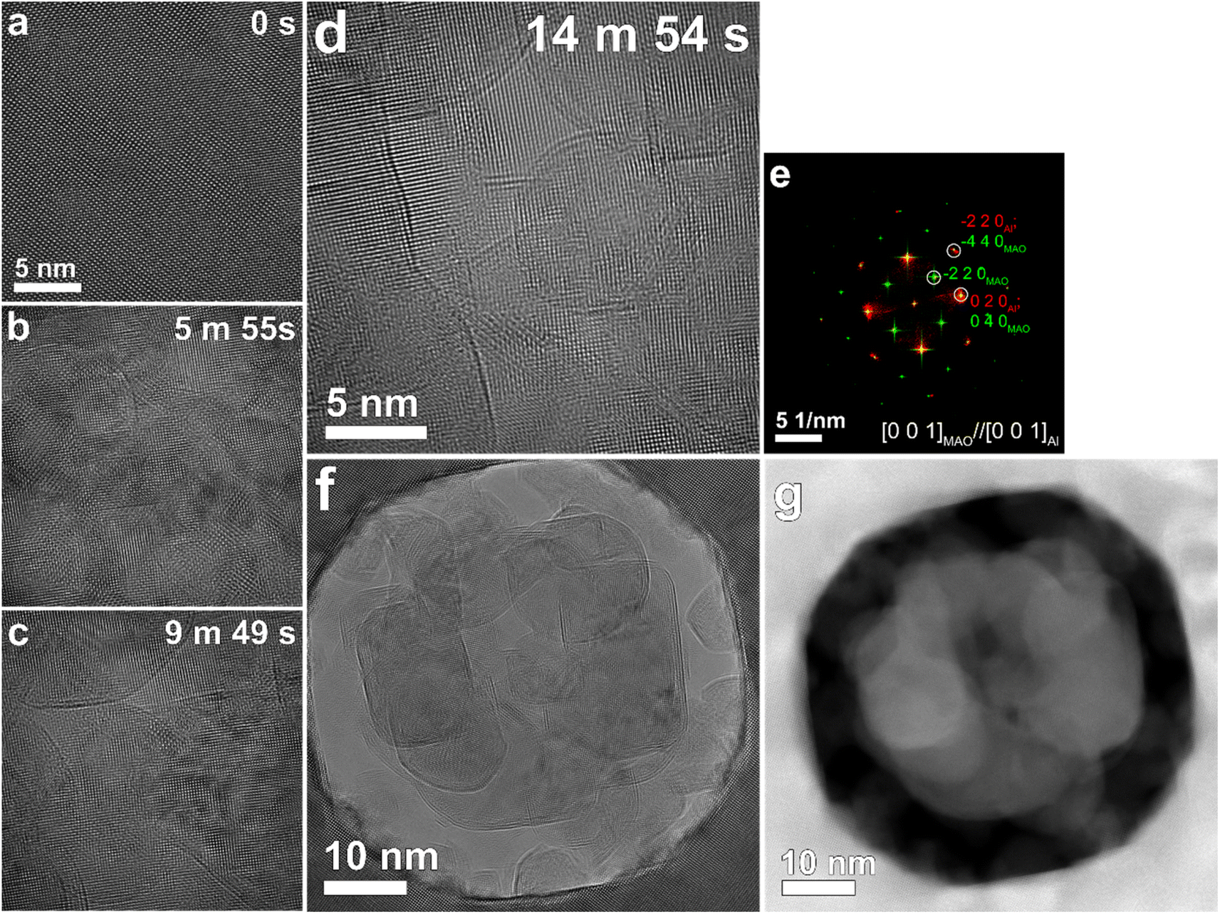 | ||
| Fig. 1 Time evolution of the irradiation behavior in the MAO specimen. Panels (a) to (d) show the evolution over time, while panel (e) is an overlay of fast Fourier transforms of the initial, unirradiated [panel (a)] and irradiated [panel (d)] regions. The green spots in (e) correspond to the initial unirradiated MAO matrix, while the red spots represent the irradiated region, revealing an orientation relationship [i.e., [0 0 1]MAO//[0 0 1]Al, (0 1 0)MAO//(0 1 0)Al]. Additionally, in (f), a lower magnification image provides a wider view after irradiation. (g) High-angle annular dark-field (HAADF) image taken at the end of the irradiation, acquired with a probe diameter of 80 pm and a dwell time of 2 μs. The irradiation time is indicated in the upper right corner of each panel, with “m” and “s” indicating minutes and seconds, respectively. | ||
In Fig. 1e, an overlay of fast Fourier transforms (FFTs) derived from the initial (Fig. 1a) and irradiated (Fig. 1d) regions reveals that the crystalline phase in the irradiated region is closely oriented to the [0 0 1] surface normal of solid Al and is nearly single-crystalline, given its lattice parameter (a = 0.405 nm). This indicates an orientation relationship between the two regions, [0 0 1]MAO//[0 0 1]Al, (0 1 0)MAO//(0 1 0)Al, which is well explained by a close match between the interplanar spacing of Al {0 2 0} (0.2025 nm) and that of MAO {0 4 0} (0.202 nm).
The thickness of the irradiated region was determined to be approximately 82 nm. This value was obtained by considering the effective atomic number of MAO (Zeff = 10) and analyzing the boxed region in the upper right corner of the low-loss EELS-SI map (Fig. 2a). The convergence and collection semi-angles used were 17.9 mrad and 38.6 mrad, respectively.
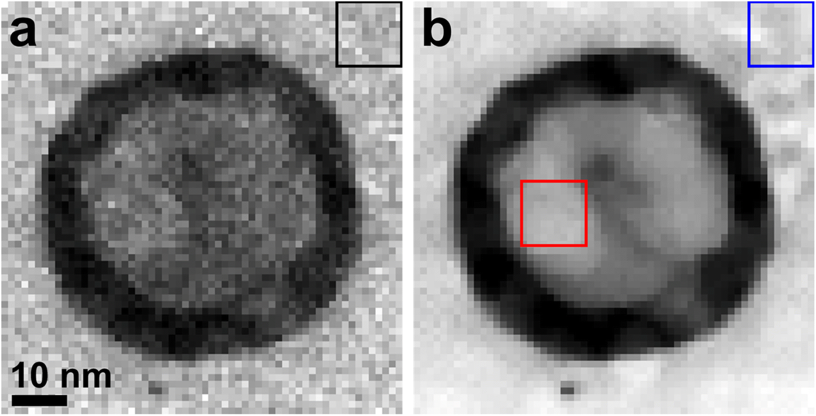 | ||
| Fig. 2 Electron energy-loss spectroscopy (EELS)-spectrum imaging (SI) maps with (a) the low-loss and (b) high-loss regions. | ||
The atomic compositions measured from the boxed areas in the irradiated region and its surroundings using the high-loss EELS-SI map (Fig. 2b) show a significant decrease in Mg (7.3%) and O (23.4%), but an increase in Al (69.3%), within the irradiated zone, as compared with those of Mg (14.2%), Al (30.9%), and O (54.9%) in the unirradiated region, as summarized in Table S1.† The composition in the unirradiated region are very similar to that of stoichiometric MgAl2O4 (14.29% Mg, 28.57% Al, and 57.14% O). This variation in elemental composition highlights a significant enrichment of Al within the irradiated region.
The compositional variations can be graphically represented by relative Al composition maps with respect to Mg and O (Fig. 3d and e), which were obtained by dividing the Al composition map (Fig. 3b) by the Mg and O maps (Fig. 3a and c, respectively).
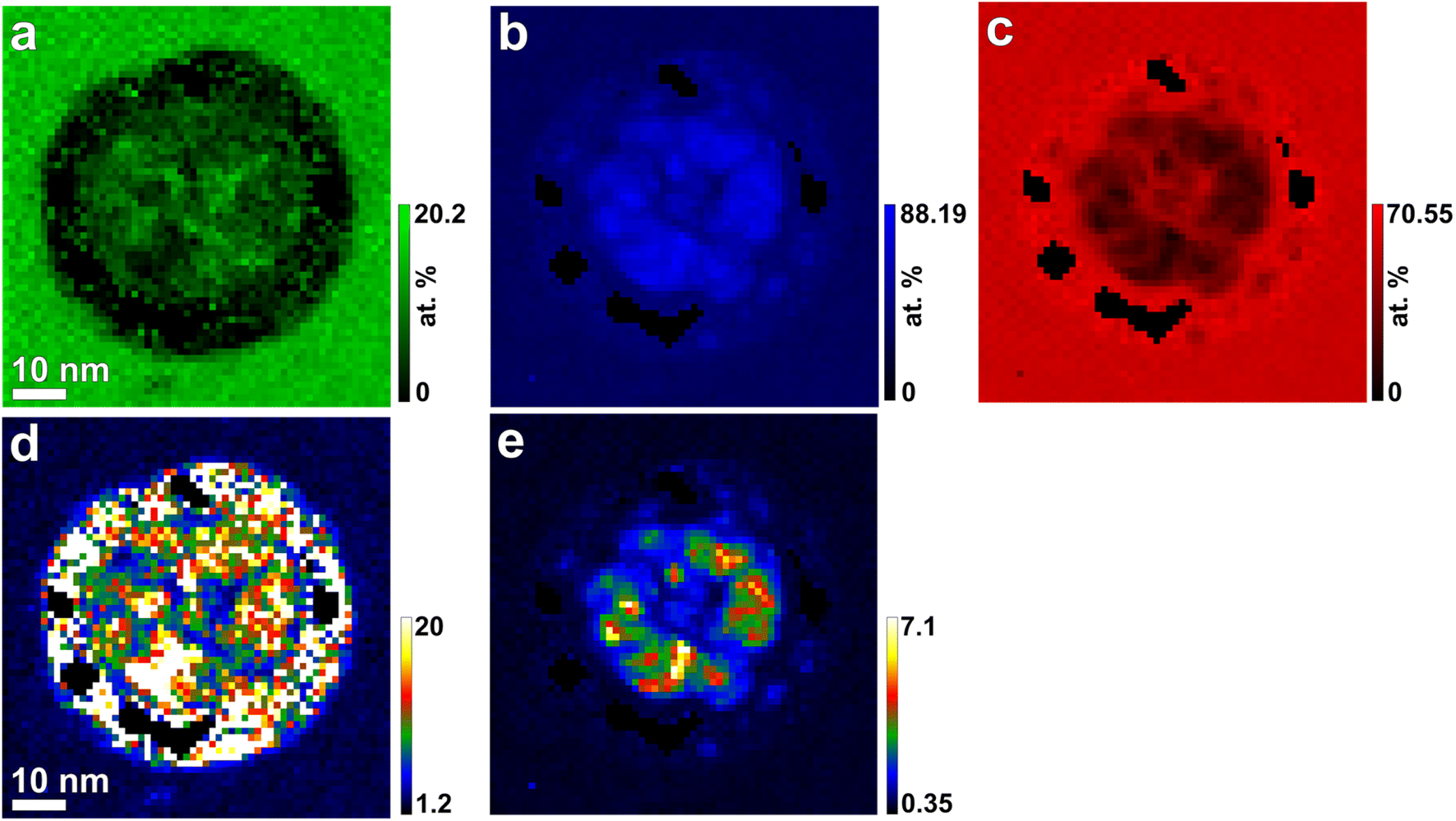 | ||
| Fig. 3 Atomic-percent composition maps of (a) Mg, (b) Al, and (c) O extracted from high-loss EELS-SI (Fig. 2b), along with derived maps showing the atomic ratios of (d) Al/Mg and (e) Al/O. | ||
The EEL spectra corresponding to the Al K, Mg K, and O K edges showed a significant change in chemical information between the unirradiated and irradiated regions. We normalized both the unirradiated and irradiated spectra with respect to their respective main peaks. The unirradiated Mg K edge exhibited typical MgAl2O4 (MAO) spectral features.14–16 The peaks between 1300 and 1320 eV, as shown in the previous work14–16 and represented by black arrows in Fig. 4a, were less visible in the unirradiated region. The Mg K edge from the irradiated region, on the other hand, lacked discernible peaks (Fig. 4a) and was weaker in intensity compared to the unirradiated region (not clearly seen in the normalized spectra). As shown in Fig. 4b, the Al K edge from the unirradiated region mirrored that of MAO.15,16 Conversely, the Al K edge from the irradiated region closely resembled that of metallic Al.17–19 In particular, the position of a saddle point for the irradiated region matched that of Al metal, as indicated by a dashed vertical line in Fig. 4b. For the O K edge (Fig. 4c), the shapes of the spectra from the unirradiated and irradiated regions were identical, showing distinct MAO features.20,21 However, the intensity of the spectra from the irradiated region was weaker than that from the unirradiated region (not clearly seen in the normalized spectra).
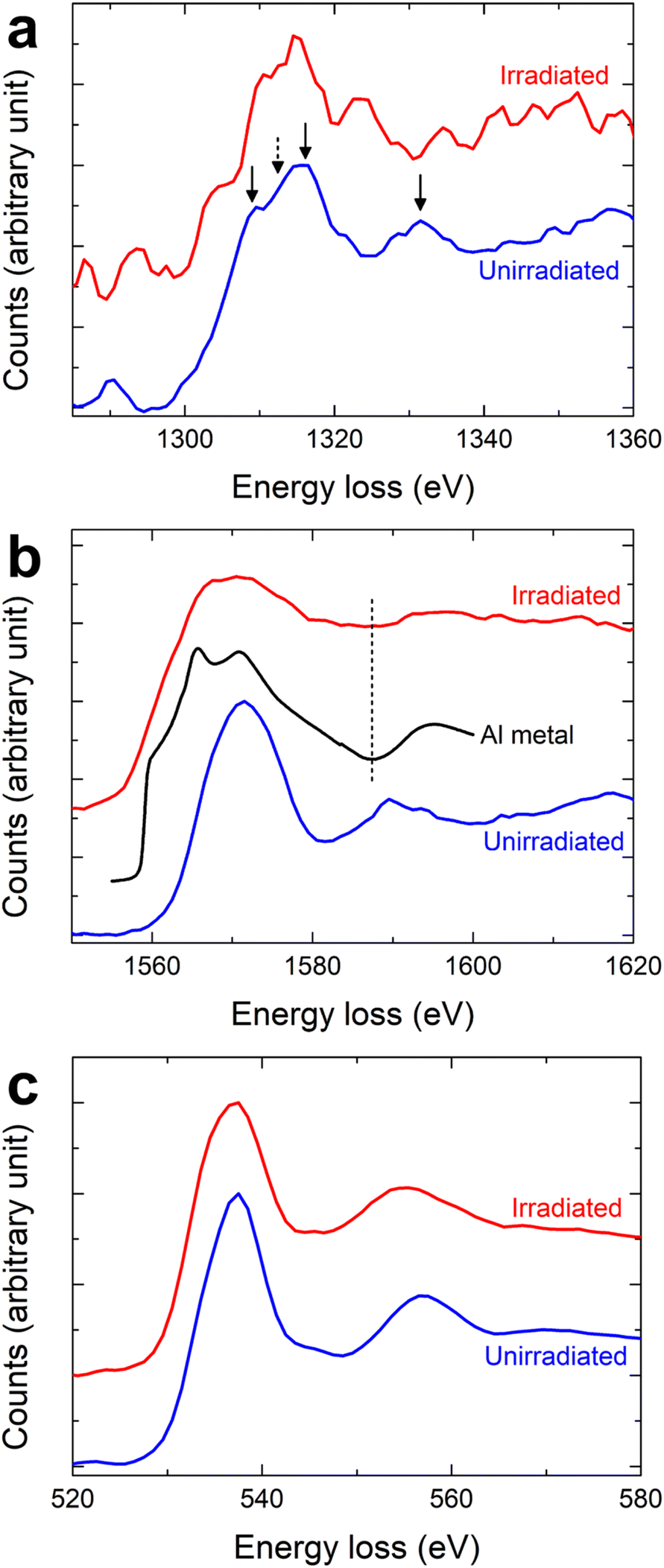 | ||
| Fig. 4 Core-loss spectra extracted from the boxed regions in Fig. 2b: (a) Mg K edge, (b) Al K edge, and (c) O K edge. For the Al K edge, to facilitate comparison with our experimental edges, the Al K edge of Al metal (99.999% purity)19 is included, as indicated by the black line in (b). | ||
Discussion
The limited contrast observed in TEM and STEM-HAADF images (Fig. 1f and g), due to the minimal difference in effective atomic number between Al (13) and MAO (10), precluded direct identification of the liquid phase using these techniques. Consequently, the identification relied primarily on two key features discernible from TEM and STEM-HAADF imaging (Fig. 1). These features include the distinctive circular morphology and the lack of interference with the crystal structure of the underlying solid phase exhibited by the observed features. This behavior is consistent with the expected properties of a liquid phase, as it would not disrupt the surface texture of the underlying solid, analogous to a water droplet on a surface. The presence of Al within the liquid phase is supported by the EELS information presented in Fig. 2–4 and Table S1.†It is reasonable to expect that upon solidification, the liquid phases would exhibit a variety of surface normal orientations. However, the observed dominance of a singular surface normal direction (Fig. 1e) in contrast to a wider range of orientations suggests that the observed circular features persisted in their liquid state. This observation further implies that the [0 0 1] pattern of Al observed in the fast Fourier transform (Fig. 1e) originates from the underlying solid substrate material.
The onset of Al segregation and melting is thought to be initiated by the dissociation of MAO under electron-beam irradiation. At first glance, this appears to be caused by knock-on atomic displacement, radiolysis, and/or sputtering. The displacement energies of Mg, Al, and O in MAO (30, 30, and 59 eV, respectively22) correspond to threshold displacement energies of 264, 288, and 326 keV, respectively, in terms of knock-on atomic displacement. As a result, knock-on atomic displacement appears less likely with 200 keV electron-beam irradiation. Instead, the segregation and subsequent melting of Al may be primarily due to radiolysis. Sputtering, on the other hand, involves the ejection of surface atoms into vacuum by bombarding the specimen with high-energy electrons. Therefore, while it may contribute to specimen thinning, its role in the dissociation is negligible. To sum up, radiolysis leads to the atomic separation of Mg and Al atoms, with O atoms being ejected into a vacuum as O2.
The Al melting phenomenon appears to be unrelated to the traces of Ga, which were most likely introduced during TEM specimen preparation by FIB. This conclusion is supported by the successful removal of Ga by post-FIB Ar ion milling, as shown in Table S2.†
To explain the melting of Al under electron-beam irradiation of MAO, we performed quantitative thermal analyses using FEA. Our investigation focused on two major effects: electron-energy loss and Auger excitation. For FEA, the geometric configuration of the matrix had a diameter of 2 μm (in the x-y plane) and a thickness of 80 nm (in the z-direction), consistent with the STEM-EELS measurement (Fig. 2a) for the thickness. A cylindrical region mirroring the irradiated region (50 nm diameter) was introduced in the center of the geometry, as shown in Fig. S2.† Taking advantage of the inherent symmetry, we modeled a quarter of the structure using finite elements, consisting of 8-node linear brick (DC3D8) elements, totaling tens of thousands. Setting the initial temperature and the temperature at the matrix edge at 293.15 K.
The energy input methods varied for different effects. To simulate the energy-loss effect, a body heat flux was applied along a line corresponding to the thickness of the irradiated region, replicating the transverse path of an incoming electron in the medium (Fig. S3a†). For the Auger effect, a heat flux was applied to a 2 nm-diameter spherical source strategically placed at the center of the layers in the irradiated region (Fig. S3b†). An energy deposition time of 10−12 s (1 ps) was used to account for electron–phonon coupling.5
Since our FEA involved modeling the irradiated region with thickness variations ranging from 80 to 10 nm, it was imperative to consider the effect of the nanoscale on thermal conductivity. It is well accepted that reducing dimensions to the nanoscale results in reduced thermal conduction due to electron scattering at surfaces.23,24 Unfortunately, there have been no reports on the nanoscale effect for MAO. Therefore, for the heat transfer analysis within the MAO layer, we relied on the findings of Negi et al.25 Their work established a consistent trend in the size effect on thermal conductivity based on experimental results across different oxides. This tendency revealed that the relative thermal conductivity to the bulk value at the nanoscale for most oxides consistently falls within a range delimited by upper and lower ratio bounds. Following the results of Negi et al.,25 we fitted two cross-plane thermal conductivities using the bulk conductivity of MAO at 300 K (8.7 W m−1 K−1)11 for each thickness, representing the potential upper and lower limits for MAO (Table S3†). Meanwhile, the bulk value was used as the in-plane thermal conductivity (Table S3†).
Understanding the influence of the energy dissipation of incoming electrons on temperature rise requires a careful study of the energy they deposit as they move through a material. The energy dissipated by these electrons can cause the temperature of the material to rise. In this investigation, we used the concept of collision stopping power,26–28 which quantifies the energy lost by an electron due to inelastic scattering within a material.
We represented the heat source as a line spanning the thicknesses studied of the MAO layer to simulate the effects of energy loss from incident electrons. MAO is characterized by a collision stopping power of 0.82 eV nm−1 for electrons with an acceleration energy of 200 keV.28 This means that an energy of 0.82 eV was deposited for every nanometer along the linear heat source (Fig. S3a†).
For the Auger effect, the calculation of deposition energies within the MAO layer involves a complicated path. Upon the incidence of an electron onto the MAO surface, the stoichiometry of MAO (1![[thin space (1/6-em)]](https://www.rsc.org/images/entities/char_2009.gif) :2:4) dictates the ensuing probabilities: 1/7 for Mg, 2/7 for Al, and 4/7 for O atoms. Further complicating matters, the cross sections for inner-shell ionization in Mg, Al, and O must be taken into account to match the probabilities of Auger events occurring. The cross sections for K-shell ionization at an acceleration energy of 200 keV are as follows:29 2.7 × 10⁻²¹ cm2 for Mg, 2 × 10⁻²¹ cm2 for Al, and 7.5 × 10⁻²¹ cm2 for O. Combining these parameters with the Auger energies of Mg (1188 eV), Al (1396 eV), and O (510 eV),30 the average deposited energy is estimated to be ∼656 eV. The full derivation is presented in ESI Section 1.†
:2:4) dictates the ensuing probabilities: 1/7 for Mg, 2/7 for Al, and 4/7 for O atoms. Further complicating matters, the cross sections for inner-shell ionization in Mg, Al, and O must be taken into account to match the probabilities of Auger events occurring. The cross sections for K-shell ionization at an acceleration energy of 200 keV are as follows:29 2.7 × 10⁻²¹ cm2 for Mg, 2 × 10⁻²¹ cm2 for Al, and 7.5 × 10⁻²¹ cm2 for O. Combining these parameters with the Auger energies of Mg (1188 eV), Al (1396 eV), and O (510 eV),30 the average deposited energy is estimated to be ∼656 eV. The full derivation is presented in ESI Section 1.†
Auger-electron energy deposition, a stochastic process, deposits less energy in the nanometer-thick layers studied here than in their bulk counterparts. Using Matthiessen's rule and considering the probability of inelastic scattering within the MAO layer at different thicknesses (80, 60, 40, 20, and 10 nm), an Auger electron is expected to deposit a part of 656.45 eV. For example, with an inelastic mean free path (IMFP) of 1.814 nm at an Auger energy of 656.45 eV for MAO,31 in the 80 nm-thick layer the Auger electron deposits a reduced energy of ∼641.90 eV, a principle applicable to the other thicknesses (see detailed derivation in Supplementary Section 2 and summarized in Table S4†). The diameter of the heat source was determined to be 2 nm (Fig. S3b†), because the inelastic mean free path ranges from 1.785 nm for the energy of 641.90 eV to 1.611 nm for 555.65 eV.31
The FEA results shown in Fig. 5a and b reveal that the energy-loss effect in specimen heating was insignificant, with the maximum temperature not reaching 300 K. In contrast, the Auger effect greatly increased the specimen temperature, exceeding the melting temperatures of Al and Mg for thinner thicknesses of the irradiated region (Fig. 5c and d). As the thickness of the irradiated region decreased from 80 to 10 nm, the maximum temperature increased from 872 K to 1274 K (Fig. 5d), most likely due to the lower cross-plane thermal conductivities (Table S3†). This decrease will cause heat accumulation and raise the specimen temperature, which was also observed in the energy-loss effect (Fig. 5b). Therefore, for each thickness, the maximum temperature calculated from the lower thermal conductivity limit exceeds the maximum temperature calculated from the upper limit (Fig. 5).
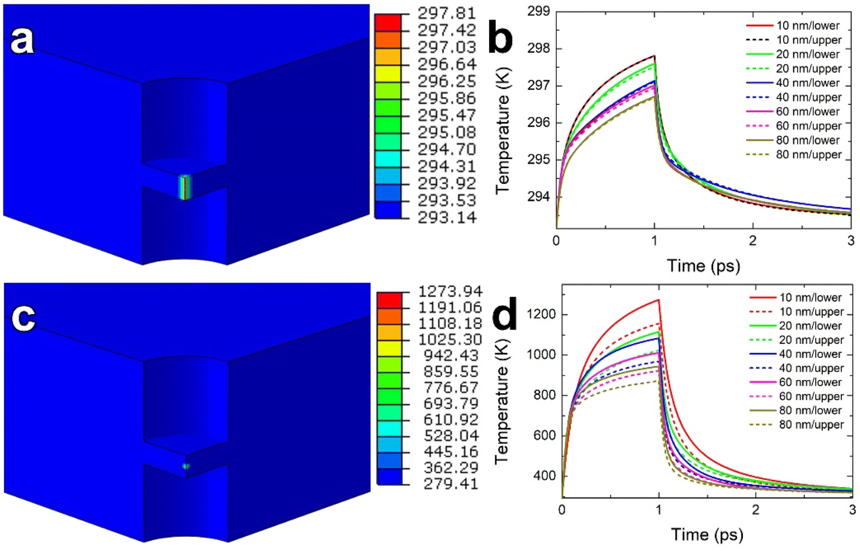 | ||
| Fig. 5 Temperature distributions at 1 ps and time evolution of the maximum temperature. (a) Quarter-symmetric temperature distribution for the energy-loss effect at 1 ps within the irradiated region (10 nm thickness at the lower-bound thermal conductivity). (b) Temperature versus time plots at the center of irradiated MAO layers of different thicknesses. (c) Quarter-symmetric temperature distribution for the Auger effect at 1 ps within the irradiated region (80 nm thickness at the lower-bound thermal conductivity. (d) Temperature versus time plots at the center of the irradiated MAO layers. | ||
The number of atoms for each element contained in the irradiated disc is shown in Table S5.† Multiplying the number of atoms by the current density used (204 A cm−2 or 1.27 × 10²¹ electrons cm−2 s−1) and the cross section of each element29 produces the corresponding number of Auger events per second for each element and its reciprocal corresponds to the time between Auger events in the MAO layers (Table S5†). The times between Auger events for the studied MAO layers with thicknesses from 10 to 80 nm are estimated to range from ∼1 μs to 10 ns. The FEA results show that the cooling rates for the Auger effect exceeded 1014 K s−1 (Fig. 5d). This implies that the specimen underwent repeated cycles of rapid melting and supercooling under electron-beam irradiation.
The faceted structure observed in the liquid droplets can be attributed to the formation of facets on the surface of the underlying solid matrix. As observed by Lee et al.,32 electron-beam irradiation induces the drilling of holes, and these holes are surrounded by energetically favorable surfaces, specifically low-index planes. Even before the drilling process, these planes begin to evolve during irradiation, resulting in surface indentation.32 The liquid droplets could become entangled in these indented surfaces, exhibiting the observed faceted shape.
In addition, the faceted appearance could also be influenced by the viscosity of the liquid metal. The angular properties of the liquid phases could be a result of viscosity effects. However, more in-depth theoretical analysis is needed to explore both explanations and to understand the complex interplay between surface dynamics and the behavior of the liquid metal under electron-beam irradiation.
The marked absence of Mg in the irradiated region compared to its unirradiated counterpart (Fig. 3d) suggests high-temperature loss, potentially due to either: (1) exceeding Mg's boiling point (1363 K) as indicated by the FEA-calculated maximum temperature (Fig. 5), or (2) Mg's much higher vapor pressure at high temperatures compared to Al (e.g., 1600 for Mg vs. 5.08 × 10⁻⁶ Pa for Al at 1000 K),33 leading to preferential evaporation under Auger-effect beam heating. Both mechanisms could contribute to the selective Mg loss. Regardless of the mechanism, very high temperatures are needed, likely caused by Auger-induced beam heating.
Note that the Auger-excitation effect becomes more pronounced at the nanoscale. As dimensions shrink to this scale, there is a simultaneous decrease in both the thermal conductivity and the number of atoms. The reduction in thermal conductivity increases heat accumulation, and the energy deposited by Auger electrons is shared by the smaller number of atoms. This combined action results in considerable specimen heating.
For the calculation of the deposited energies, we primarily focused on K-shell ionization for Mg, Al, and O. Mg and Al also exhibit LMM Auger events, but their energies (48 and 70 eV, respectively)30 are significantly lower than their KLL counterparts (1188 and 1396 eV)30 despite higher cross sections for L-shell ionization (3 × 10⁻¹⁹ cm2 for Mg and 2 × 10⁻¹⁹ cm2 for Al at 200 keV) than those for K-shell ionization.29 This energy difference led us to prioritize KLL Auger events for Mg and Al in our heating energy deposition calculations.
We acknowledge the existence of other secondary electrons, categorized as slow and fast. However, due to their low energies (∼50 eV) and even lower cross sections than inner-shell ionizations,2 slow secondary electrons were excluded. Due to their high energies (up to 50% of the incident beam energy),2 fast secondary electrons exhibit collision stopping powers comparable to those of the incident electron, leading to negligible specimen heating. Consequently, this study solely focuses on KLL Auger events for Mg, Al, and O as the primary source of heating during electron microscopy.
Conclusions
Our observations suggest that Auger excitation, rather than the traditional electron-energy loss mechanism, is the primary contributor to specimen heating during Al melting in TEM. This finding challenges current understanding of beam heating in TEM and necessitates reinterpretation of beam-irradiation phenomena occurring in many systems. Furthermore, the ability to form liquid metal microstructures with electron beams demonstrated here suggests the development of advanced materials for microfluidic devices with precisely controlled flow patterns at the nanoscale. Liquid metals have high electrical and thermal conductivity as well as exceptional deformability.34,35 In this research, we propose to utilize these characteristics through electron-beam irradiation to enhance the surface engineering of different compounds. This opens up new possibilities for creating flexible electronics, a project that is currently underway.Author contributions
Sung Bo Lee: conceptualization, data curation, TEM, funding acquisition, supervision, writing original draft, writing review; Jun Young Chae: FEA analysis; Heung Nam Han: analysis, funding acquisition, writing review.Conflicts of interest
There are no conflicts to declare.Acknowledgements
S. B. L. received financial support from the Korea Basic Science Institute under the R&D program (Project No. C330430) supervised by the Ministry of Science and ICT (MSIT, Republic of Korea). S. B. L. was supported by the National Research Foundation of Korea (NRF) grant funded by the Ministry of Education [RS-2023-00240516 (RIAM)]. H. N. H. was supported by the National Research Foundation of Korea (NRF) grant funded by the Korea government (MSIT) (NRF-2021R1A2C3005096).References
- R. F. Egerton, P. Li and M. Malac, Radiation damage in the TEM and SEM, Micron, 2004, 35, 399–409 CrossRef CAS.
- D. B. Williams and C. B. Carter, Transmission Electron Microscopy, Springer, New York, 2009 Search PubMed.
- R. F. Egerton, Control of radiation damage in the TEM, Ultramicroscopy, 2013, 127, 100–108 CrossRef CAS PubMed.
- P. A. Buffat, Dynamical behavior of nanocrystals in transmission electron microscopy: size, temperature or irradiation effects, Philos. Trans. R. Soc., A, 2003, 361, 291–295 CrossRef CAS.
- P. Williams, Motion of small gold clusters in the electron microscope, Appl. Phys. Lett., 1987, 50, 1760–1762 CrossRef CAS.
- J. M. Pénisson, Y. Lereah and B. Pantel, Low temperature HREM observations of structural fluctuations in small particles: evidence for a thermally activated process, Microsc. Res. Tech., 1997, 36, 438–439 CrossRef.
- T. Ben-David, Y. Lereah, G. Deutscher, J. M. Pénisson, A. Bourret, R. Kofman and P. Cheyssac, Correlated orientations in nanocrystal fluctuations, Phys. Rev. Lett., 1997, 78, 2585–2587 CrossRef.
- D. Ugarte, Revisiting the structural instability observed in small particles in the electron microscope, Z. Phys. D, 1993, 28, 177–181 CrossRef CAS.
- Y. Lereah, R. Kofman, J. M. Pénisson, G. Deutscher, P. Cheyssac, T. Ben-David and A. Bourret, Time-resolved electron microscopy studies of nanoparticles and their melting, Philos. Mag. B, 2011, 81, 1801–1819 CrossRef.
- S. B. Lee, S.-G. Kang, J. Jung, S. Sung, S. J. Yoo and H. N. Han, Lattice shear and non-random rotation of Au nanoparticles under electron-beam irradiation, Acta Mater., 2022, 241, 118387 CrossRef CAS.
- C.-M. Ni, H.-W. Fan, X.-D. Wang and M. Yao, Thermal conductivity prediction of MgAl2O4: a non-equilibrium molecular dynamics calculation, J. Iron Steel Res. Int., 2020, 27, 500–505 CrossRef CAS.
- D. C. Harris, L. F. Johnson, R. Seaver and T. Lewis, Optical and thermal properties of spinel with revised (increased) absorption at 4 to 5 μm wavelengths and comparison with sapphire, Opt. Eng., 2013, 52, 087113 CrossRef.
- S. Klemme and M. Ahrens, Low-temperature heat capacities of MgAl2O4 and spinels of the MgCr2O4–MgAl2O4 solid solution, Phys. Chem. Miner., 2007, 34, 59–72 CrossRef CAS.
- N. Trcera, D. Cabaret, S. Rossano, F. Farges, A.-M. Flank and P. Lagarde, Experimental and theoretical study of the structural environment of magnesium in minerals and silicate glasses using X-ray absorption near-edge structure, Phys. Chem. Miner., 2009, 36, 241–257 CrossRef CAS.
- D. R. Neuville, D. de Ligny, L. Cormier, G. S. Henderson, J. Roux, A.-M. Flank and P. Lagarde, The crystal and melt structure of spinel and alumina at high temperature: An in-situ XANES study at the Al and Mg K-edge, Geochim. Cosmochim. Acta, 2009, 73, 3410–3422 CrossRef CAS.
- D. de Ligny, D. R. Neuville, A.-M. Flank and P. Lagarde, Structure of spinel at high temperature using in-situ XANES study at the Al and Mg K-edge, J. Phys.: Conf. Ser., 2009, 190, 012178 CrossRef.
- M. Mogi, T. Yamamoto, T. Mizoguchi, K. Tatsumi, S. Yoshioka, S. Kameyama, I. Tanaka and H. Adachi, Theoretical Investigation of Al K-edge X-ray Absorption Spectra of Al, AlN and Al2O3, Mater. Trans., 2004, 45, 2031–2034 CrossRef CAS.
- J. C. Sánchez-López, A. Caballero and A. Fernández, Characterisation of passivated aluminium nanopowders: an XPS and TEM/EELS study, J. Eur. Ceram. Soc., 1998, 18, 1195–1200 CrossRef.
- P. Ewels, T. Sikora, V. Serin, C. P. Ewels and L. Lajaunie, A complete overhaul of the electron energy-loss spectroscopy and X-ray absorption spectroscopy database: eelsdb.eu, Microsc. Microanal., 2016, 22, 717–724 CrossRef CAS.
- S. Köstlmeier and C. Elsässer, Ab initio calculation of near-edge structures in electron-energy-loss spectra for metal-oxide crystals, Phys. Rev. B, 1999, 60, 14025 CrossRef.
- S. Nyquist and U. Hålenius, An EELS study of near edge structures of the oxygen K-edge in spinels, Phys. Chem. Miner., 2014, 41, 255–265 CrossRef CAS.
- G. P. Pells, Radiation effects and damage mechanisms in ceramic insulators and window materials, J. Nucl. Mater., 1988, 155–157, 67–76 CrossRef.
- N. Stojanovic, D. H. S. Maithripala, J. M. Berg and M. Holtz, Thermal conductivity in metallic nanostructures at high temperature: Electrons, phonons, and the Wiedemann-Franz law, Phys. Rev. B, 2010, 82, 075418 CrossRef.
- Z. Tong, S. Li, X. Ruan and H. Bao, Comprehensive first-principles analysis of phonon thermal conductivity and electron-phonon coupling in different metals, Phys. Rev. B, 2019, 100, 144306 CrossRef CAS.
- A. Negi, A. Rodriguez, X. Zhang, A. H. Comstock, C. Yang, D. Sun, X. Jiang, D. Kumah, M. Hu and J. Liu, Thickness- dependent thermal conductivity and phonon mean free path distribution in single-crystalline barium titanate, Adv. Sci., 2023, 10, 2301273 CrossRef CAS PubMed.
- D. C. Joy and S. Luo, An empirical stopping power relationship for low-energy electrons, Scanning, 1989, 11, 176–180 CrossRef.
- J. R. Lowney, Monte Carlo simulation of scanning electron microscope signals for lithographic metrology, Scanning, 1996, 18, 301–306 CrossRef CAS.
- M. J. Berger, J. S. Coursey, M. A. Zucker and J. Chang, Stopping Power and Range Tables for Electrons, Positrons, and Helium Ions, National Institute of Standards and Technology (NIST) Standard Database, 2017, vol. 124, https://www.nist.gov/pml/stopping-power-range-tables-electrons-protons-and-helium-ions Search PubMed.
- X. Llovet, F. Salvat, D. Bote, F. Salvat-Pujol, A. Jablonski and C. J. Powell, NIST Database of Cross Sections for Inner-Shell Ionization by Electron or Positron Impact, Version 1.0, SRD 164, National Institute of Standards and Technology, Gaithersburg, Maryland, 2014 Search PubMed.
- K. D. Childs, B. A. Carlson, L. A. LaVanier, J. F. Moulder, D. F. Paul, W. F. Stickle and D. G. Watson, Handbook of Auger Electron Spectroscopy: A Book of Reference Data for Identification and Interpretation in Auger Electron Spectroscopy, ed. C. L. Hedberg, 3rd edn, Physical Electronics, Inc., Eden Prairie, MN, 1995 Search PubMed.
- C. J. Powell and A. Jablonski, NIST Electron Inelastic-Mean-Free-Path Database-Version 1.2, SRD 71, National Institute of Standards and Technology, Gaithersburg, MD, 2010 Search PubMed.
- S. B. Lee, S. J. Yoo, J. Jung and H. N. Han, Surface roughening and filling of nanoholes in Au surfaces under electron-beam irradiation, Acta Mater., 2021, 220, 117280 CrossRef CAS.
- https://www2.iap.tuwien.ac.at/www/surface/vapor_pressure .
- T. Daeneke, K. Khoshmanesh, N. Mahmood, I. A. de Castro, D. Esrafilzadeh, S. J. Barrow, M. D. Dickey and K. Kalanta-zadeh, Liquid metals: fundamentals and applications in chemistry, Chem. Soc. Rev., 2018, 47, 4073–4111 RSC.
- A. Zavabeti, J. Z. Ou, B. J. Carey, N. Syed, R. Orrell-Trigg, E. L. H. Mayes, C. Xu, O. Kavehei, A. P. O'Mullane, R. B. Kaner, K. Kalantar-zadeh and T. Daeneke, A liquid metal reaction environment for the room-temperature synthesis of atomically thin metal oxides, Science, 2017, 358, 332–335 CrossRef CAS PubMed.
Footnote |
| † Electronic supplementary information (ESI) available. See DOI: https://doi.org/10.1039/d4na00011k |
| This journal is © The Royal Society of Chemistry 2024 |