
 Open Access Article
 This Open Access Article is licensed under a Creative Commons Attribution-Non Commercial 3.0 Unported Licence
Wetting and strain engineering of 2D materials on nanopatterned substrates†
Davoud
Adinehloo
 a,
Joshua R.
Hendrickson
b and
Vasili
Perebeinos
*a
a,
Joshua R.
Hendrickson
b and
Vasili
Perebeinos
*a
aDepartment of Electrical Engineering, University at Buffalo, Buffalo, NY 14228, USA. E-mail: vasilipe@buffalo.edu
bSensors Directorate, Air Force Research Laboratory, Wright-Patterson AFB, Ohio 45433, USA
First published on 3rd April 2024
Abstract
The fascinating realm of strain engineering and wetting transitions in two-dimensional (2D) materials takes place when placed on a two-dimensional array of nanopillars or one-dimensional rectangular grated substrates. Our investigation encompasses a diverse set of atomically thin 2D materials, including transition metal dichalcogenides, hexagonal boron nitride, and graphene, with a keen focus on the impact of van der Waals adhesion energies to the substrate on the wetting/dewetting behavior on nanopatterned substrates. We find a critical aspect ratio of the nanopillar or grating heights to the period of the pattern when the wetting/dewetting transition occurs. Furthermore, energy hysteresis analysis reveals dynamic detachment and re-engagement events during height adjustments, shedding light on energy barriers of 2D monolayer transferred on patterned substrates. Our findings offer avenues for strain engineering in 2D materials, leading to promising prospects for future technological applications.
1 Introduction
Two-dimensional (2D) materials have garnered immense attention due to their exceptional electronic,1–3 optical,4,5 and mechanical6,7 properties. These atomically thin materials exhibit remarkable promise for various applications, from high-performance electronics to advanced photonics.8,9 Particularly fascinating is their ability to function as single-photon emitters (SPEs), a role that holds great promise in the field of quantum information science and technology.10–12In the realm of quantum technology, the quest for SPEs has been ongoing, and 2D materials, such as transition metal dichalcogenides (TMD) and hexagonal boron nitride (hBN), have emerged as promising candidates to fulfill this role.13–16 Localization of excitons within 2D materials, induced by strain or defects, has been identified as the primary source of such photon emission.13,16–19 Several articles have reported local strain-induced SPEs, providing valuable insight into their behavior.20–22
In fact, it is of paramount importance to highlight that the intricate microscopic mechanisms that govern the formation of strain-induced SPEs in 2D materials remain a topic of ongoing investigation.23 Further elucidation of these mechanisms is vital to advance our understanding of SPEs in 2D materials, with direct implications for the development of reliable and efficient SPEs integrated into quantum technologies.22,24–26
The mechanical properties of 2D materials have been extensively explored.27 These properties play an important role in shaping the electronic and optoelectronic performance of 2D materials.28–33 The adhesion energies of 2D materials to substrates, for example, have been reported in various materials: 6 to 28 meV Å−2 for graphene on silicon oxide,6,34–37 9.4 meV Å−2 for graphene on silicon,38,39 1.12 meV Å−2 for MoS2 on PMDS,40 6.3 meV Å−2 for MoS2 on Al2O3,41 and 5 meV Å−2 for MoS2 on SiO2.41 Studies on the folding behavior of 2D materials,42 and investigations of heterostructures involving 2D materials,43 provide valuable information on their mechanical characteristics. Furthermore, specific structural arrangements have been examined, such as a graphene membrane stacked on triangular nanopillars,44,45 sinusoidally corrugated surfaces,46 and bubble structures.47–53 However, it is essential to note that while several studies have addressed the mechanical behavior of 2D materials, there is still a gap in our understanding regarding factors such as geometrical configuration, interfacial adhesion energy, and the period of the patterned structure, which warrants further investigation.
In this study, we offer a significant step towards advancing our ability to precisely manipulate local strain in 2D materials by gaining a profound understanding of their mechanical behavior when interfaced with various substrates. The first configuration that we consider involves an intricate examination of the geometric variations of 2D materials, incorporating a two-dimensional array of hard-wall rounded nanopillars (as depicted in Fig. 1(a)). The intricate surface profile of each pillar, characterized by a half-semicircular structure with height equal to the radius, that is, h = r (as depicted in Fig. 1(c)), is expertly captured. The second configuration features a rectangular one-dimensional substrate grating overlaid with a 2D material filling in the formed trenches, as visualized in Fig. 1(b). Remarkably, the inherent complexity of these configurations is elegantly distilled into a concise 1D formulation, as illustrated in both Fig. 1(c) and (d). Through this research, we provide a deeper understanding of the mechanical response of 2D materials, opening up new avenues for precision engineering applications.
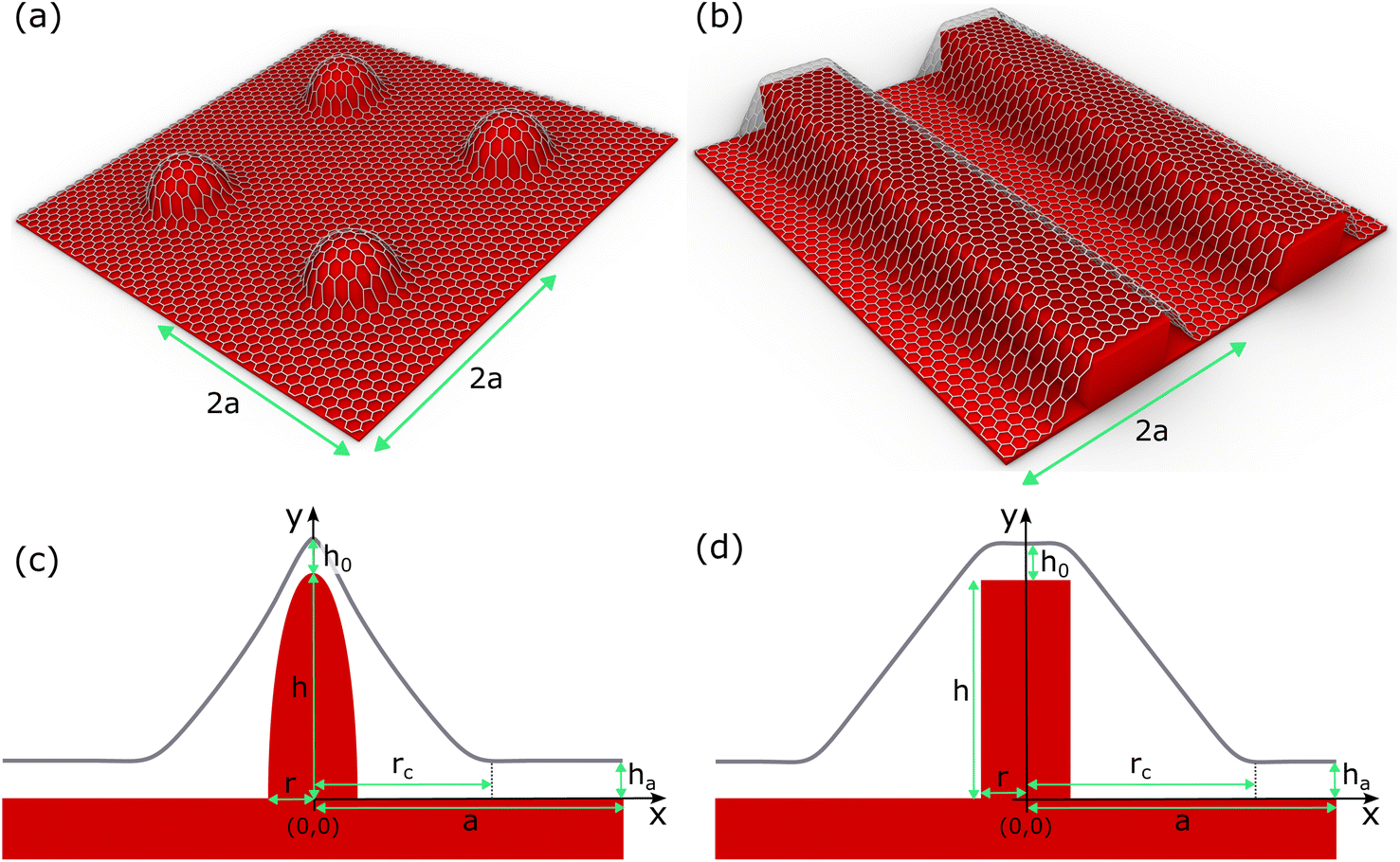 | ||
| Fig. 1 Schematic representations of two structural configurations: (a) a two-dimensional array of rounded nanopillars and (b) a rectangular one-dimensional substrate grating. Both nanopatterned substrates are coated with a monolayer of 2D material. (c) and (d) Provide the vertical cross-sectional view of the 2D material when placed on nanopillars and rectangular grating, respectively. The key parameters include the period 2a of the patterned substrate, h for the height of the nanostructure, 2r representing the diameter of the nanopillar or the width of the grating, and ha denoting the height of the 2D material at the edge of the unit cell at x = a. | ||
2 Theoretical framework
In this investigation, we present a rigorous theoretical framework to quantify the total energy per unit cell area of the patterned structure. This energy is expressed as follows:| E = Estrain + Ebending + Eadhesion | (1) |
To assess the strain experienced by the 2D material, we utilize the following equation:
 | (2) |
We assumed here that the area of 2D material equals the unit cell area of 2a × 2a and no sliding is allowed, such that any tilt of 2D material results in the local strain given by eqn (2).
3 Results and discussion
Fig. 2 illustrates the mechanical response of MoSe2, which serves as a representative example of 2D materials when strategically placed on a two-dimensional array of nanopillars or on a rectangular one-dimensional substrate grating. Since the adhesion energy can be engineered by choosing a 2D material and substrate, we present our results for an experimentally accessible range of adhesion energies γ. Note that the mechanical properties of the materials under consideration here are independent of the orientation, i.e., the armchair or zigzag.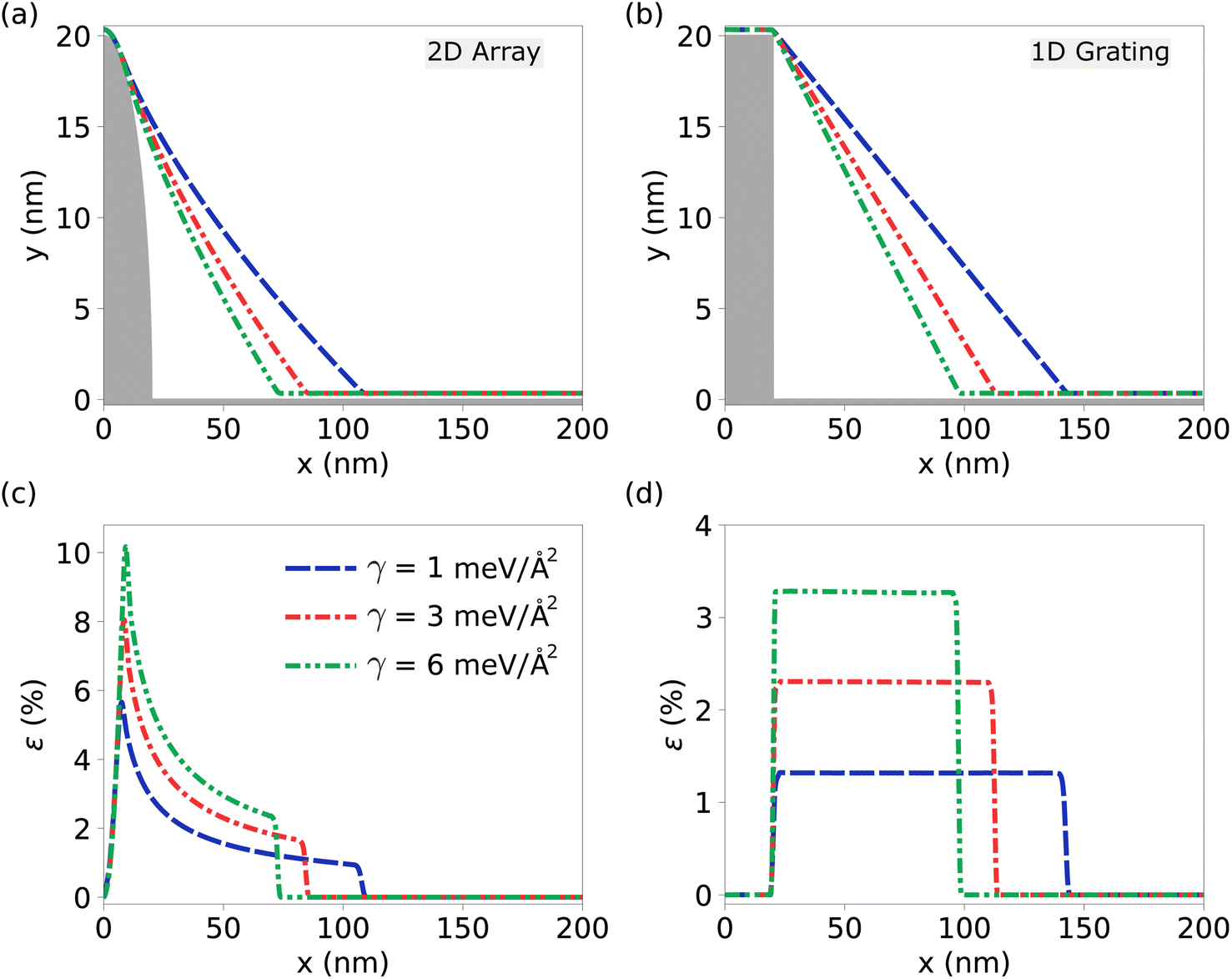 | ||
| Fig. 2 Engineering MoSe2 structure on two-dimensional nanopillar array and one-dimensional grating configurations. (a) Demonstrates the customized behavior of MoSe2 on nanopillar array, while (b) illustrates the controlled modulation of the MoSe2 structure on grated substrate with varying interfacial adhesion energy (γ). (c) Unveils the intricate strain distribution within the MoSe2 structures on nanopillars, and (d) presents the comprehensive strain distribution in the MoSe2 structures in the grated substrates over a range of γ levels. These figures collectively highlight the profound impact of the interfacial adhesion energy (γ) on MoSe2 positioning and the distribution of strain. A constant values of a of 200 nm is maintained in all configurations to ensure a consistent basis for comparison. The gray area in (a) and (b) represents the nanostructured substrate. | ||
In Fig. 2(a), we observe the precise tailoring of MoSe2 behavior when placed on a nanopillar array. This figure provides visual evidence of van der Waals interactions that govern the material's positioning atop the nanopillars. Manipulation of the MoSe2 geometry on one-dimensional substrate grating with varying values γ is demonstrated in Fig. 2(b). This highlights the versatility of MoSe2 in adapting to different interfacial adhesion energies.
Fig. 2(c) provides an in-depth exploration of the strain distribution within the MoSe2 structures on nanopillars. It becomes evident that the strained area of the 2D material can be manipulated by varying the interfacial adhesion energy. As γ increases or decreases, the extent of the strain within the material adjusts accordingly, leading to a controlled modulation of the strained area. This tunability is of paramount importance in tailoring the mechanical response of 2D materials for specific applications, particularly in SPEs applications.
In Fig. 2(d), we extend a similar analysis to MoSe2 structures within grating configurations, providing a detailed view of its response to varying γ values. Interestingly, a distinct behavior is observed in grated structures: the strain in the strained area remains relatively constant until the 2D material fully contacts the substrate in the trenches. This phenomenon suggests that grating configurations exhibit a unique mechanical response characterized by a sudden change in strain behavior upon contact, distinct from the gradual modulation observed in nanopillar arrays.
To dig deeper into the response of 2D materials placed in nanopillar arrays and patterned substrates, we introduce the concept of a critical distance, denoted rc. This critical distance represents the point at which the strain levels approach near-zero values. Fig. 3 presents the ratio of the critical distance rc to h, together with the maximum and average strain values as functions of γ.
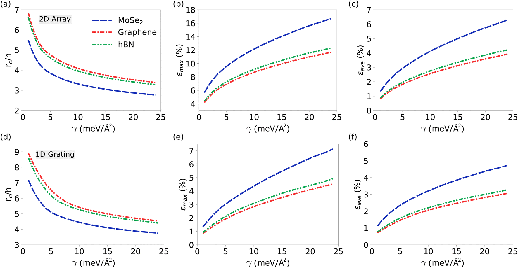 | ||
| Fig. 3 The evolution of the critical distance ratio (rc) relative to the heights of the nanopillars and the depths of the grating in response to the variations γ between different 2D materials and substrates is presented in (a) and (d), respectively. The maximum strain within the 2D material is analyzed in (b) for nanopillar array configurations and (e) for grating configurations as a function of the interfacial adhesion energy. The average strain within the 2D material is illustrated in (c) for the nanopillar array and in (f) for grating scenarios. | ||
Fig. 3(a) and (d) depict the ratio of rc/h versus interfacial adhesion energy for the case of the nanopillar array and the patterned substrate, respectively. In particular, as γ increases, this ratio decreases consistently. Importantly, this trend remains consistent over varying periods. Furthermore, the ratio exhibits variations between different materials, primarily due to differences in their Young modulus and bending stiffness, as detailed in Table S1 in ESI.†54
The evolution of maximum strain as a function of γ is depicted in Fig. 3(b) and (e) for nanopillar array and the patterned substrate, respectively. It becomes evident that as γ increases, the maximum strain exhibits a corresponding increase, due to the changes in the shape of the 2D material induced by stronger adhesion between its layers. Additionally, it should be noted that the maximum strain for 2D materials on the nanopillar arrays is approximately twice that observed for 2D materials atop one-dimensional patterned substrates. It is worth mentioning that prior studies have reported strains exceeding 10% in materials such as MoS2,27,55 graphene,56,57 and hBN.58,59 Therefore, the majority of our results remain within the elastic limit.
Since exciton emission can occur from different locations in 2D material, we introduce the concept of average strain as follows:
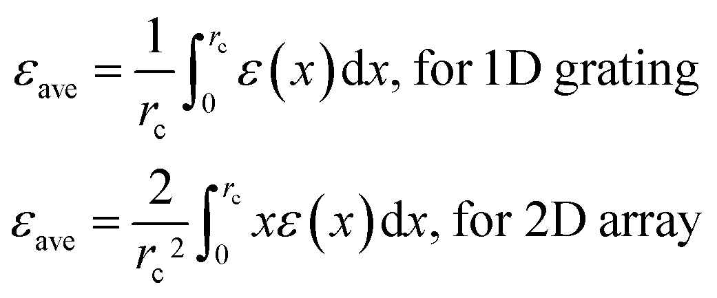 | (3) |
Fig. 4 presents a detailed analysis of the energy variations within the sample structures. Specifically, Fig. 4(a) and (b) provide information on the energy hysteresis observed with respect to changes in ha. In particular, as the parameter ha increases, an intriguing phenomenon unfolds: the 2D material gradually disengages from the substrate, leading to a gradual increase in overall energy. However, a critical threshold of ha is reached, beyond which a remarkable event occurs, the complete detachment of the 2D material from the substrate. This detachment event is characterized by a sharp and pronounced drop in total energy. Beyond this critical threshold, further increases in ha no longer significantly impact the energy of the system as it stabilizes in a detached state. Conversely, when reducing ha, the energy landscape exhibits a distinct behavior. Initially, as ha decreases, the energy remains relatively constant until it reaches a lower value. Subsequently, a departure from this equilibrium occurs, resulting in an increase in energy. Ultimately, the energy reaches the activation energy, denoted Ea, signifying the point at which the 2D material re-establishes contact with the substrate. This reengagement prompts a swift and substantial drop in energy as the structure strives to achieve its optimized configuration. It is noteworthy that as the adhesion energy increases, larger values of ha are required to detach the 2D material from the substrate. This is attributed to the higher attraction energy between the substrate and the 2D layer.
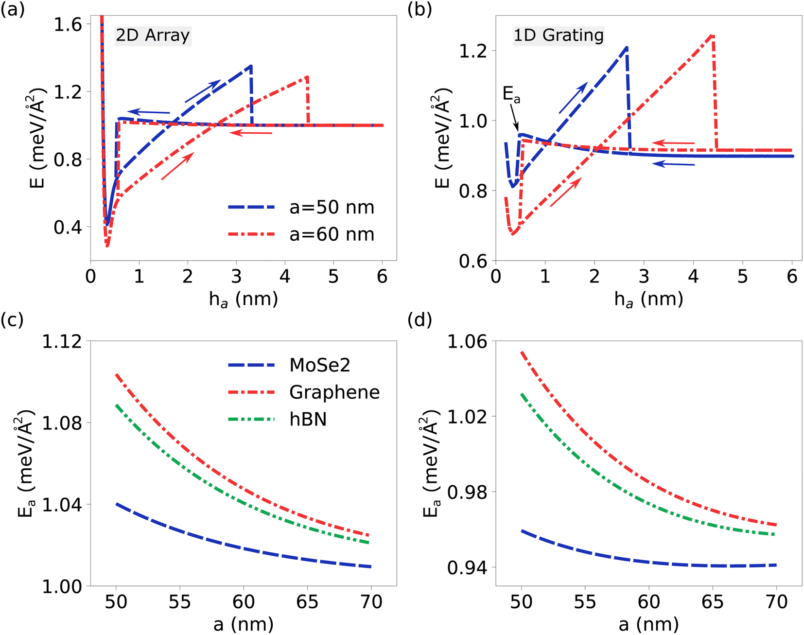 | ||
| Fig. 4 Energy hysteresis and analysis of the activation energy. (a) and (b) Show the energy hysteresis for the nanopillar array configuration and the grated substrate, respectively, as a function of ha for different lengths of the period. (c) and (d) Show the activated energy for the nanopillar array configuration and the grated substrate configuration, respectively, as a function of periods across diverse materials. The adhesion energy is set to 1 meV A−2 and h = 5 nm in both cases. These comprehensive analyses provide deep insight into the energy behavior of these structures across various parameters. | ||
Turning our attention to Fig. 4(c) and (d), these plots provide a detailed analysis of the activation energy as a function of the period in a range of materials. A clear and consistent trend emerges: as the period increases, the activation energy exhibits a consistent decrease. This observation underscores the intriguing relationship between the period and the energy required for structural relaxation. Specifically, longer periods are associated with a reduced demand for energy during the relaxation process, a phenomenon of significance in the study of material behavior.
4 Conclusion
In summary, our advanced theoretical framework provides a comprehensive understanding of the mechanics of 2D material membranes when transferred to different patterned substrates, such as nanopillar array and grating structures. It elucidates the critical role of the interfacial adhesion energy (γ) in the governing behavior of these materials. As γ increases, significant alterations are observed in the strain, critical period, and energy profiles, highlighting the sensitivity of 2D materials to this parameter and offering the prospect of precise engineering for customized nanoscale applications. A notable outcome of this study is the concept of a critical aspect ratio of the height of the nanostructure to the period (rc), which emerges as a key metric that characterizes the response of the system. rc varies with both γ and the specific material, providing valuable information on how 2D materials adapt and interact with different substrate environments.The analysis of energy hysteresis reveals intriguing detachment and reengagement events as the height of the 2D material on the substrate changes. These events are reflected in sharp fluctuations in energy profiles, emphasizing the dynamic nature of these systems and the energy barriers associated with structural rearrangements. Furthermore, the investigation of activation energy demonstrates that it decreases with a larger period, shedding light on the role of the pattern period in shaping material behavior. This advanced framework not only enhances our understanding of 2D material mechanics but also presents opportunities for precision engineering, paving the way for tailored nanoscale materials and devices with specific mechanical properties, thus contributing to the evolving field of 2D materials and their potential technological applications.
Conflicts of interest
There are no conflicts to declare.Acknowledgements
We gratefully acknowledge John Schaibley for useful discussions. We acknowledge the support of the Air Force Office of Scientific Research under award number FA9550-22-1-0312 and the computational facilities of the Center for Computational Research at the University of Buffalo (https://hdl.handle.net/10477/79221). J. R. H. acknowledges support from the Air Force Office of Scientific Research (Program Manager, Dr Gernot Pomrenke) under award number FA9550-20RYCOR059.References
- G. Wang, A. Chernikov, M. M. Glazov, T. F. Heinz, X. Marie, T. Amand and B. Urbaszek, Rev. Mod. Phys., 2018, 90, 021001 Search PubMed.
- Q. H. Wang, K. Kalantar-Zadeh, A. Kis, J. N. Coleman and M. S. Strano, Nat. Nanotechnol., 2012, 7, 699–712 Search PubMed.
- P. Avouris, Z. Chen and V. Perebeinos, Nat. Nanotechnol., 2007, 2, 605–615 Search PubMed.
- Q. Ma, G. Ren, K. Xu and J. Z. Ou, Adv. Opt. Mater., 2021, 9, 2001313 Search PubMed.
- J. You, S. Bongu, Q. Bao and N. Panoiu, Nanophotonics, 2019, 8, 63–97 Search PubMed.
- D. Akinwande, C. J. Brennan, J. S. Bunch, P. Egberts, J. R. Felts, H. Gao, R. Huang, J.-S. Kim, T. Li, Y. Li, K. M. Liechti, N. Lu, H. S. Park, E. J. Reed, P. Wang, B. I. Yakobson, T. Zhang, Y.-W. Zhang, Y. Zhou and Y. Zhu, Extreme Mechanics Letters, 2017, 13, 42–77 Search PubMed.
- C. Androulidakis, K. Zhang, M. Robertson and S. Tawfick, 2D Materials, 2018, 5, 032005 Search PubMed.
- M. C. Lemme, D. Akinwande, C. Huyghebaert and C. Stampfer, Nat. Commun., 2022, 13, 1392 Search PubMed.
- M. Ponnusamy, K. Ramya, V. Sivasankaran, H. Farmani and A. Farmani, J. Mater. Res., 2022, 1–14 Search PubMed.
- I. Aharonovich, D. Englund and M. Toth, Nat. Photonics, 2016, 10, 631–641 Search PubMed.
- A. F. Koenderink, A. Alù and A. Polman, Science, 2015, 348, 516–521 Search PubMed.
- M. D. Eisaman, J. Fan, A. Migdall and S. V. Polyakov, Rev. Sci. Instrum., 2011, 82, 071101 Search PubMed.
- A. N. Abramov, I. Y. Chestnov, E. S. Alimova, T. Ivanova, I. S. Mukhin, D. N. Krizhanovskii, I. A. Shelykh, I. V. Iorsh and V. Kravtsov, Nat. Commun., 2023, 14, 5737 Search PubMed.
- P. Tonndorf, R. Schmidt, R. Schneider, J. Kern, M. Buscema, G. A. Steele, A. Castellanos-Gomez, H. S. J. van der Zant, S. M. de Vasconcellos and R. Bratschitsch, Optica, 2015, 2, 347–352 Search PubMed.
- Y.-M. He, G. Clark, J. R. Schaibley, Y. He, M.-C. Chen, Y.-J. Wei, X. Ding, Q. Zhang, W. Yao and X. Xu, et al. , Nat. Nanotechnol., 2015, 10, 497–502 Search PubMed.
- N. Mendelson, D. Chugh, J. R. Reimers, T. S. Cheng, A. Gottscholl, H. Long, C. J. Mellor, A. Zettl, V. Dyakonov and P. H. Beton, et al. , Nat. Mater., 2021, 20, 321–328 Search PubMed.
- A. R.-P. Montblanch, D. M. Kara, I. Paradisanos, C. M. Purser, M. S. Feuer, E. M. Alexeev, L. Stefan, Y. Qin, M. Blei and G. Wang, et al. , Commun. Phys., 2021, 4, 119 Search PubMed.
- G. Kim, H. M. Kim, P. Kumar, M. Rahaman, C. E. Stevens, J. Jeon, K. Jo, K.-H. Kim, N. Trainor, H. Zhu, B.-H. Sohn, E. A. Stach, J. R. Hendrickson, N. R. Glavin, J. Suh, J. M. Redwing and D. Jariwala, ACS Nano, 2022, 16, 9651–9659 Search PubMed.
- L. Linhart, M. Paur, V. Smejkal, J. Burgdörfer, T. Mueller and F. Libisch, Phys. Rev. Lett., 2019, 123, 146401 Search PubMed.
- A. Branny, S. Kumar, R. Proux and B. D. Gerardot, Nat. Commun., 2017, 8, 15053 Search PubMed.
- Y. Liu, W. Huang, T. Gong, Y. Su, H. Zhang, Y. He, Z. Liu and B. Yu, Nanoscale, 2017, 9, 17459–17464 Search PubMed.
- C. Palacios-Berraquero, D. M. Kara, A. R.-P. Montblanch, M. Barbone, P. Latawiec, D. Yoon, A. K. Ott, M. Loncar, A. C. Ferrari and M. Atatüre, Nat. Commun., 2017, 8, 15093 Search PubMed.
- S. I. Azzam, K. Parto and G. Moody, Appl. Phys. Lett., 2021, 118, 240502 Search PubMed.
- J. An, X. Zhao, Y. Zhang, M. Liu, J. Yuan, X. Sun, Z. Zhang, B. Wang, S. Li and D. Li, Adv. Funct. Mater., 2022, 32, 2110119 Search PubMed.
- H. Tian, M. L. Chin, S. Najmaei, Q. Guo, F. Xia, H. Wang and M. Dubey, Nano Res., 2016, 9, 1543–1560 Search PubMed.
- S. G. Carter, T. M. Sweeney, M. Kim, C. S. Kim, D. Solenov, S. E. Economou, T. L. Reinecke, L. Yang, A. S. Bracker and D. Gammon, Nat. Photonics, 2013, 7, 329–334 Search PubMed.
- S. Bertolazzi, J. Brivio and A. Kis, ACS Nano, 2011, 5, 9703–9709 Search PubMed.
- M. T. Mahmud, D. Zhai and N. Sandler, Nano Lett., 2023, 23, 7725–7732 Search PubMed.
- Y. Lei, T. Zhang, Y.-C. Lin, T. Granzier-Nakajima, G. Bepete, D. A. Kowalczyk, Z. Lin, D. Zhou, T. F. Schranghamer, A. Dodda, A. Sebastian, Y. Chen, Y. Liu, G. Pourtois, T. J. Kempa, B. Schuler, M. T. Edmonds, S. Y. Quek, U. Wurstbauer, S. M. Wu, N. R. Glavin, S. Das, S. P. Dash, J. M. Redwing, J. A. Robinson and M. Terrones, ACS Nanosci. Au, 2022, 2, 450–485 Search PubMed.
- D. Adinehloo and M. Fathipour, J. Appl. Phys., 2015, 118, 234305 Search PubMed.
- S. B. Touski and N. Ghobadi, J. Phys. D: Appl. Phys., 2021, 54, 485302 Search PubMed.
- H. Adib, M. Mazaherifar, S. B. Touski and S. Mohajerzadeh, IEEE Trans. Electron Devices, 2023, 1–7 Search PubMed.
- N. Hasani, A. Rajabi-Maram and S. B. Touski, J. Phys. Chem. Solids, 2023, 174, 111131 Search PubMed.
- T. C. Nguyen, M. Otani and S. Okada, Phys. Rev. Lett., 2011, 106, 106801 Search PubMed.
- N. G. Boddeti, S. P. Koenig, R. Long, J. Xiao, J. S. Bunch and M. L. Dunn, J. Appl. Mech., 2013, 80, 040909 Search PubMed.
- S. R. Na, J. W. Suk, R. S. Ruoff, R. Huang and K. M. Liechti, ACS Nano, 2014, 8, 11234–11242 Search PubMed.
- S. P. Koenig, N. G. Boddeti, M. L. Dunn and J. S. Bunch, Nat. Nanotechnol., 2011, 6, 543–546 Search PubMed.
- Z. Dai, N. Lu, K. M. Liechti and R. Huang, Curr. Opin. Solid State Mater. Sci., 2020, 24, 100837 Search PubMed.
- Z. Zong, C.-L. Chen, M. R. Dokmeci and K.-t. Wan, J. Appl. Phys., 2010, 107, 026104 Search PubMed.
- C. J. Brennan, J. Nguyen, E. T. Yu and N. Lu, Adv. Mater. Interfaces, 2015, 2, 1500176 Search PubMed.
- D. A. Sanchez, Z. Dai, P. Wang, A. Cantu-Chavez, C. J. Brennan, R. Huang and N. Lu, Proc. Natl. Acad. Sci. U. S. A., 2018, 115, 7884–7889 Search PubMed.
- J. Zhao, Q. Deng, T. H. Ly, G. H. Han, G. Sandeep and M. H. Rümmeli, Nat. Commun., 2015, 6, 8935 Search PubMed.
- J. Yu, E. Han, M. A. Hossain, K. Watanabe, T. Taniguchi, E. Ertekin, A. M. van der Zande and P. Y. Huang, Adv. Mater., 2021, 33, 2007269 Search PubMed.
- S. P. Milovanović, L. Covaci and F. M. Peeters, J. Appl. Phys., 2019, 125, 082534 Search PubMed.
- J. Mao, S. P. Milovanović, M. Anđelković, X. Lai, Y. Cao, K. Watanabe, T. Taniguchi, L. Covaci, F. M. Peeters and A. K. Geim, et al. , Nature, 2020, 584, 215–220 Search PubMed.
- M. Neek-Amal and F. M. Peeters, Phys. Rev. B, 2012, 85, 195445 Search PubMed.
- E. Blundo, A. Surrente, D. Spirito, G. Pettinari, T. Yildirim, C. A. Chavarin, L. Baldassarre, M. Felici and A. Polimeni, Nano Lett., 2022, 22, 1525–1533 Search PubMed.
- E. Blundo, T. Yildirim, G. Pettinari and A. Polimeni, Phys. Rev. Lett., 2021, 127, 046101 Search PubMed.
- J. Yu, S. Kim, E. Ertekin and A. M. van der Zande, ACS Appl. Mater. Interfaces, 2020, 12, 10801–10808 Search PubMed.
- R. Villarreal, P.-C. Lin, F. Faraji, N. Hassani, H. Bana, Z. Zarkua, M. N. Nair, H.-C. Tsai, M. Auge, F. Junge, H. C. Hofsaess, S. De Gendt, S. De Feyter, S. Brems, E. H. Åhlgren, E. C. Neyts, L. Covaci, F. M. Peeters, M. Neek-Amal and L. M. C. Pereira, Nano Lett., 2021, 21, 8103–8110 Search PubMed.
- Y. Chen, Y. Wang, W. Shen, M. Wu, B. Li, Q. Zhang, S. Liu, C. Hu, S. Yang, Y. Gao and C. Jiang, ACS Nano, 2022, 16, 16271–16280 Search PubMed.
- D. Lloyd, X. Liu, N. Boddeti, L. Cantley, R. Long, M. L. Dunn and J. S. Bunch, Nano Lett., 2017, 17, 5329–5334 Search PubMed.
- M. Gastaldo, J. Varillas, Á. Rodríguez, M. Velický, O. Frank and M. Kalbáč, npj 2D Mater. Appl., 2023, 7, 71 Search PubMed.
- See ESI† which includes Ref. 60–63.
- T.-J. Ko, M. Wang, C. Yoo, E. Okogbue, M. A. Islam, H. Li, M. S. Shawkat, S. S. Han, K. H. Oh and Y. Jung, J. Phys. D: Appl. Phys., 2020, 53, 313002 Search PubMed.
- H. H. Perez Garza, E. W. Kievit, G. F. Schneider and U. Staufer, Nano Lett., 2014, 14, 4107–4113 Search PubMed.
- K. S. Kim, Y. Zhao, H. Jang, S. Y. Lee, J. M. Kim, K. S. Kim, J.-H. Ahn, P. Kim, J.-Y. Choi and B. H. Hong, Nature, 2009, 457, 706–710 Search PubMed.
- A. Falin, Q. Cai, E. J. Santos, D. Scullion, D. Qian, R. Zhang, Z. Yang, S. Huang, K. Watanabe and T. Taniguchi, et al. , Nat. Commun., 2017, 8, 15815 Search PubMed.
- S. Roy, X. Zhang, A. B. Puthirath, A. Meiyazhagan, S. Bhattacharyya, M. M. Rahman, G. Babu, S. Susarla, S. K. Saju and M. K. Tran, et al. , Adv. Mater., 2021, 33, 2101589 Search PubMed.
- Y. Yang, X. Li, M. Wen, E. Hacopian, W. Chen, Y. Gong, J. Zhang, B. Li, W. Zhou, P. M. Ajayan, Q. Chen, T. Zhu and J. Lou, Adv. Mater., 2017, 29, 1604201 Search PubMed.
- C. Lee, X. Wei, J. W. Kysar and J. Hone, Science, 2008, 321, 385–388 Search PubMed.
- P. M. Morse, Phys. Rev., 1929, 34, 57–64 Search PubMed.
- V. Perebeinos and J. Tersoff, Nano Lett., 2014, 14, 4376–4380 Search PubMed.
Footnote |
| † Electronic supplementary information (ESI) available. See DOI: https://doi.org/10.1039/d3na01079a |
| This journal is © The Royal Society of Chemistry 2024 |