
 Open Access Article
 This Open Access Article is licensed under a Creative Commons Attribution-Non Commercial 3.0 Unported Licence
Facile synthesis of nanostructured Ni/NiO/N-doped graphene electrocatalysts for enhanced oxygen evolution reaction†
Roshni
Madampadi
a,
Avit Bhogilal
Patel
b,
C. P.
Vinod
 cd,
Ritu
Gupta
be and
Dinesh
Jagadeesan
*a
cd,
Ritu
Gupta
be and
Dinesh
Jagadeesan
*a
aDepartment of Chemistry, Indian Institute of Technology Palakkad, Kerala 678 623, India. E-mail: d.jagadeesan@iitpkd.ac.in
bDepartment of Chemistry, Indian Institute of Technology Jodhpur, Jodhpur 342037, India
cCatalysis and Inorganic Chemistry Division, CSIR-National Chemical Laboratory, Pune 411008, India
dAcademy of Scientific and Innovative Research (AcSIR), Ghaziabad 201002, India
eDepartment of Chemistry, Indian Institute of Technology Delhi, New Delhi 110016, India
First published on 22nd April 2024
Abstract
Electrocatalysts containing a Ni/NiO/N-doped graphene interface have been synthesised using the ligand-assisted chemical vapor deposition technique. NiO nanoparticles were used as the substrate to grow N-doped graphene by decomposing vapours of benzene and N-containing ligands. The method was demonstrated with two nitrogen-containing ligands, namely dipyrazino[2,3-f:2′,3′-h]quinoxaline-2,3,6,7,10,11-hexacarbonitrile (L) and melamine (M). The structure and composition of the as-synthesized composites were characterized by XRD, Raman spectroscopy, SEM, TEM and XPS. The composite prepared using the ligand L had NiO sandwiched between Ni and N-doped graphene and showed an overpotential of 292 mV at 10 mA cm−2 and a Tafel slope of 45.41 mV dec−1 for the OER, which is comparable to the existing noble metal catalysts. The composite prepared using the ligand M had Ni encapsulated by N-doped graphene without NiO. It showed an overpotential of 390 mV at 10 mA cm−2 and a Tafel slope of 78.9 mV dec−1. The ligand-assisted CVD route demonstrates a facile route to control the microstructure of the electrocatalysts.
1. Introduction
Electrocatalytic water splitting is a promising and scalable technology to renewably produce green hydrogen. The success of this technology hinges on the development of efficient, low-cost electrocatalysts for the sluggish oxygen evolution reaction (OER). Although noble metals are outstanding in their performance, their high cost is an impediment to the translational success of the technology. Extensive studies on transition metal oxides based on Co,1,2 Ni,3–5 Mn,6,7 Fe,8 Cu,9,10 and Zn11 in the form of simple,12 doped,13–15 and mixed oxides,16,17 layered double hydroxides18,19 in nanostructured forms,20,21 porous architectures22 or nanocomposites23–27 underscore their prominence as economically viable alternatives to noble metal-based electrocatalysts. Conventionally, the nanocomposites of transition metals and oxides with graphene have been attractive as they offered a good electrochemical performance due to high electrical conductivity, surface area, and specific capacitance (2573 F g−1) with low fabrication costs.20,21,28–31 Defects in the form of heteroatomic doping on graphene have been shown not only to improve the conductivity but also increase the adsorption of reactants. In recent years, the crucial role of the microstructure of catalysts on the performance has come to the fore. Besides the right composition, the microstructure of an electrocatalyst has been recognized to enhance seamless electronic interaction between its different components, that eventually results in superior reaction kinetics. Particularly, the metal–metal oxide interfaces on electrocatalysts are interesting as they favour the formation of oxygen vacancies, which can activate the reactants, as well as aid in an efficient charge transfer.32,33 Considering these results, structured nanocomposites such as metal/metal oxide/N-doped graphene is likely to hold the key to higher efficiency due to favorable chemisorption as well as charge transfer kinetics in the OER.31 Although microstructured electrocatalysts are an interesting target, their synthesis in a scalable fashion is a non-trivial subject. Solution-based chemical synthetic routes adopted to obtain such N-doped graphene–metal/metal oxide nanocomposites typically involve the preparation of graphene/graphene oxide or vice versa followed by the deposition of metal oxide nanoparticles on its surface, followed by a redox step to obtain the required microstructure. Such methods result in poor interfacial interaction and hence higher performance is not fully recognized. A facile method to synthesize composites with control over the microstructure is critical to realize better OER catalysts. In this work, we have synthesized the composites of Ni/NiO and N-doped graphene using the chemical vapor deposition (CVD) technique. In this scalable route, carbon can be intimately deposited on the surface of a substrate due to thermal decomposition of volatile carbon precursors. Among various possible transition metals, Ni was chosen due to the high solubility of carbon in the metal lattice under high temperatures that eventually precipitates on cooling to form graphene. The minimal lattice mismatch between Ni and the graphene is another factor to be considered to avoid lattice strains along the interfaces.34–37 The latter has been shown to result in an efficient charge transfer across the interface.38,39 Such an advantage is usually sacrificed in other bottom-up chemical synthetic routes, where interfaces are poorly structured.To obtain the nanostructured catalyst, NiO nanoparticles (ESI) were used as the substrate instead of conventionally employed metallic Ni foil or plates. The NiO nanoparticles have a higher surface area than Ni foil and hence the resultant composite was envisaged to have a higher surface area. Typically, in a CVD method, nitrogen is doped into graphene by passing nitrogen-containing gaseous precursors or vapours of nitrogen containing organic precursors into the hot reaction zone along with the carbon precursor diluted in a carrier gas. Alternatively, solid nitrogen precursors may be sublimed or directly deposited on the substrate.40 In this work, the doping of nitrogen was attempted in a single step by vaporizing a solution of nitrogen-containing ligands dissolved in benzene. The vapour of the solution of benzene was generated using a liquid vaporizer and carried to the reaction site with a flow of H2. The method offers a facile route to control the microstructure of a nanocomposite electrocatalyst.
2. Experimental section
2.1. Materials
All chemicals (nickel nitrate, D-glucose, CTAB, and KOH) were purchased from Sigma-Aldrich. Ni foam was purchased from The Electrode Store, India, with 99.99% purity.2.2. Preparation of N-doped graphene-decorated nickel nanoparticles
2.3. Characterization
A powder X-ray diffractometer (model: Rigaku Smart Lab XRD) with a Cu Kα source (λ = 0.154 nm) operated at a voltage of 45 kV and a current of 200 mA was used to identify the crystalline phases of the material. The sample scan was done in the range of 2θ = 10–90° with a step size of 0.02. An FT-IR spectrometer (IR Tracer 100, Shimadzu Scientific Instruments) was used to understand bonding characteristics in N-doped graphene. A Raman spectrophotometer (model: Horiba Labram HR Evo) was used to analyze the spectra in the 100–3000 cm−1 range, employing a 532 nm ULF laser source. The morphology of the samples was characterized using a Field Emission Scanning Electron Microscope (FESEM). The elemental dispersion was confirmed by EDS mapping associated with FE-SEM. The binding energies of the elements present in the catalyst were analyzed by X-ray photoelectron spectroscopy (Thermo Fisher Scientific Instruments UK, model K ALPHA+) with a monchromatic Al Kα X-ray source with 6 mA beam current and 12 kV operating voltage. Transmission electron microscopy (TEM) was performed using a Talos 2000S G2 FEG with an EDS detector. High-resolution TEM (HRTEM) pictures and electron diffraction (ED) patterns were analyzed by Gatan GMS 3 software (open source).2.4. Electrochemical measurements
All electrochemical measurements were performed on a CH electrochemical workstation (CHI 660E). The commercially available Ni foam electrode (0.5 cm2) was sonicated for 5 min in acetone, 3 M HCl, and deionized water to clean the surface oxide layers. After cleaning, the Ni foam was dried in a vacuum chamber for 6 h at 60 °C. The working electrodes were prepared by drop coating a 10 mg dispersion of each electrocatalyst (NiFL and NiFMF) in a mixture of 1 mL of water and ethanol (1![[thin space (1/6-em)]](https://www.rsc.org/images/entities/char_2009.gif) :1) and 10 μL of Nafion. After drop coating, the electrodes were vacuum-dried. All electrochemical measurements were performed with a three electrode geometry containing an Ag/AgCl reference electrode and Pt wire as a counter electrode in 1 M KOH (pH = 14) solution. Linear sweep voltammetry (LSV) measurements were conducted at a scan rate of 5 mV s−1 in the voltage range of 0 to 1 V versus an Ag/AgCl electrode and converted to a reversible hydrogen electrode (RHE) using the following equation (eqn (1)).
:1) and 10 μL of Nafion. After drop coating, the electrodes were vacuum-dried. All electrochemical measurements were performed with a three electrode geometry containing an Ag/AgCl reference electrode and Pt wire as a counter electrode in 1 M KOH (pH = 14) solution. Linear sweep voltammetry (LSV) measurements were conducted at a scan rate of 5 mV s−1 in the voltage range of 0 to 1 V versus an Ag/AgCl electrode and converted to a reversible hydrogen electrode (RHE) using the following equation (eqn (1)).| E(RHE) = EAg/AgCl + 0.05912 pH + 0.197 V | (1) |
| Cs = ∫IdV/ΔV × ν × A | (2) |
 , where F is the Faraday constant, n is the number of active sites, n = Q/2F, calculated by performing CV in the non-faradaic region, and I is current at a specific overpotential. Electrochemical impedance spectroscopy (EIS) was performed at 0.6 V versus Ag/AgCl electrode with a potential amplitude of 5 mV in the AC frequency range from 0.1 to 105 Hz.
3. Results and discussion
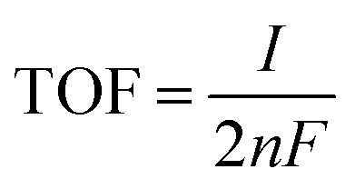
The molecular structures of ligands L and M that are introduced with an intention to dope nitrogen in the graphene differed in the nature of the nitrogen as well as the nitrogen-to-carbon ratio (Fig. 1a). XRD patterns of the composites NiFL and NiFMF prepared in the presence of the ligands L and M, respectively are shown in Fig. 1b. The peak at 2θ = 26.2° is indexed to graphite (JCPDS No.: 56-0159) in both samples. Particularly, the peak in NiFMF is broadened significantly more compared to NiFL indicating the presence of a fewer layers of graphene in the NiFMF. This intriguing observation can be explained based on the effect of the ligands on the physical properties of the solution of benzene. The concentration-dependent changes to the physical properties of benzene are expected in the presence of solutes such as L or M. The concentration of M was kept significantly high compared to L in order to keep the nitrogen content in the solutions approximately close. Due to this, the boiling point of the benzene solution containing M is expected to be higher compared to that of the solution containing L. As a result, at 353 K, the rate of vaporization of benzene from solution M is likely to be lower compared to that in the solution containing L. Thus, the strong graphitic peak in NiFL is due to the availability of a larger concentration of benzene available for decomposition at the reaction site (in comparison to NiFMF). In addition to the number of layers of graphene, the ligands and their concentration also had a stark influence on the chemical composition of the composite. Peaks at 2θ = 44.4, 62.8, and 76.3° corresponded to metallic nickel (JCPDS No.: 04-0850), and peaks at 2θ = 37.2, 43.2, and 62.8° corresponded to NiO (JCPDS No.: 01-071-1179). Interestingly, the composition of the composites differed with the ligand employed. NiFL contained Ni, NiO, and graphene, whereas NiFMF contained only Ni and graphene.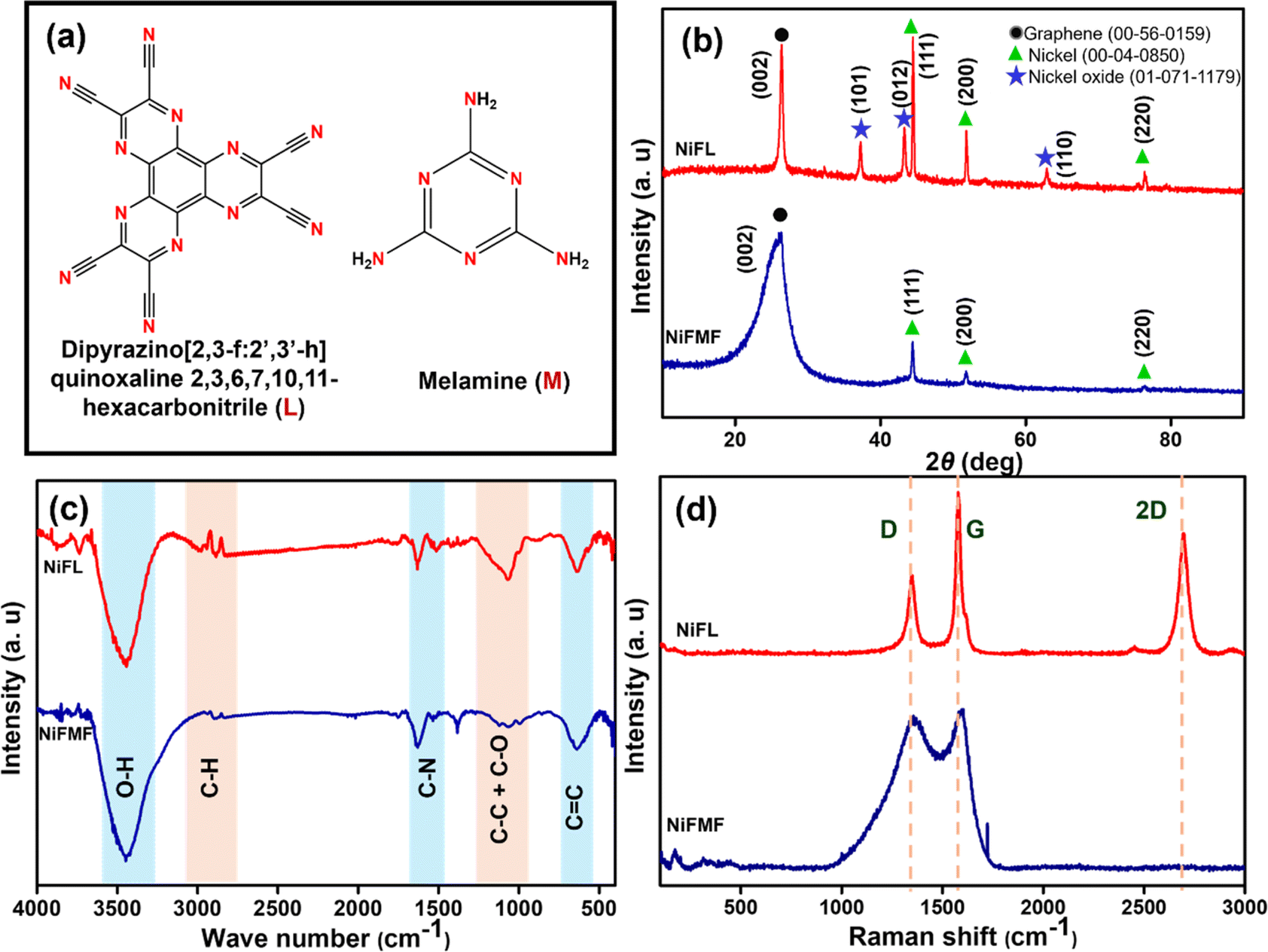 | ||
Fig. 1 (a) The molecular structures of the ligands L and M, (b) XRD pattern of NiFL (red) and NiFMF (blue) with  graphite, graphite,  nickel and nickel and  nickel oxide, (c) IR spectra of NiFL (red) and NiFMF (blue), and (d) Raman spectra of NiFL (red) and NiFMF (blue). nickel oxide, (c) IR spectra of NiFL (red) and NiFMF (blue), and (d) Raman spectra of NiFL (red) and NiFMF (blue). | ||
Although the substrate is NiO in both cases, the difference in the final composition of the composite hints at the differences in the surface chemical reactions leading to the growth of the graphene. The thermal profile and the reaction atmosphere of H2 adopted in the synthesis favourably reduces NiO to metallic Ni prior to the starting of the CVD growth. The presence of ligand M in benzene vapour has favored the reduced phase in Ni, even after the completion of the growth of graphene. However, the presence of ligand L in benzene vapour has probably favoured the partial oxidation of the Ni back to NiO. This is likely to be along the interface between the metal and the graphene. The IR spectra shown in Fig. 1c confirmed the presence of nitrogen in graphene with C–N stretches in both NiFL and NiFMF samples.44 Consistent with our suspicion that the ligand L may have favored the oxidation of Ni to NiO, the presence of oxygenated species as characterized by the C–O around 1065 cm−1 is stronger in the case of NiFL.
The quality of the graphene was further probed using Raman spectroscopy. In general, the Raman spectrum of the graphene shows three bands (D, G, and 2D bands), characteristic of few-layered graphene. The D and 2D bands are due to second-order double resonance by zone boundary phonons, and the G band is due to the doubly degenerate E2g phonons at the Brillouin zone.41 The Raman spectrum of NiFL, as shown in Fig. 1d, shows all three bands. In addition to the three bands, NiFL also shows a small shoulder peak around 1610 cm−1, corresponding to the D′ band ascribed to the intravalley, defect-induced, double-resonance processes.41 The fact that the 2D band is present in NiFL suggested a unique structural difference between NiFL and NiFMF. In NiFL, probably NiO is sandwiched between Ni and graphene so that Ni is not in direct contact with the graphene. Importantly, the 2D band in Ni/graphene composites is subdued strongly suggesting a direct contact between Ni and carbon.42 Importantly, this band is present in NiFL. Further, in NiFMF, the D and G bands merged, and the 2D band was absent. The higher number of defects causes the D band to have a broader appearance, which consequently leads to its overlap with the G band. The absence of the 2D band also indicates higher defect concentrations43 in graphene. In conclusion, the characterization data suggests that NiFL is a multilayered composite with a Ni/NiO/N-doped graphene structure, while NiFMF is fewer layered, defect-rich, N-doped graphene encapsulating Ni nanoparticles with an interface of Ni/N-doped graphene.
The elemental composition on the surface of NiFL and NiFMF is analyzed using XPS. The O 1s spectra comprised peaks corresponding to three different oxygen species in the sample. Generally, the peak in the range of 527.7–530 eV corresponds to the lattice oxygen (OL), and the peak in the range of 531.1–532 eV corresponds to the oxygen vacancy (OV).45 In Fig. 2a, the peak for OV in NiFL is found at 531 eV. The peak at 532.2 eV is ascribed to functionalized oxygen (OF) such as –COO– or O![[double bond, length as m-dash]](https://www.rsc.org/images/entities/char_e001.gif) C–O on graphene.46 In Fig. 2c, the O 1s spectrum of NiFMF is deconvoluted to two peaks corresponding to adsorbed oxygen species (OA) and OF on carbon. As expected, the peak due to OV is absent in NiFMF. The C 1s spectra of both samples show signals due to C–N species (285.8 eV) confirming the doping of the nitrogen.47 Attempts to record the N 1s spectra to determine the nature of nitrogen in the carbon matrix did not yield satisfactory data in both the cases. This intriguing observation is probably due to the heterogeneity in the concentration of nitrogen in the graphene shell. XPS, being a surface-sensitive technique, gives information on the nitrogen content pertaining to the surface of a few nm (1–5 nm) depth. It is likely that the nitrogen ligand vaporized in larger concentrations during the initial reaction periods. This increases the concentration of N-doping on graphene layers closer to the surface of NiO substrate. As the reaction proceeded, the concentration of the ligands in the vapor phase may have decreased, leading to a decreased doping. This may have resulted in a low concentration of nitrogen on the surface.
C–O on graphene.46 In Fig. 2c, the O 1s spectrum of NiFMF is deconvoluted to two peaks corresponding to adsorbed oxygen species (OA) and OF on carbon. As expected, the peak due to OV is absent in NiFMF. The C 1s spectra of both samples show signals due to C–N species (285.8 eV) confirming the doping of the nitrogen.47 Attempts to record the N 1s spectra to determine the nature of nitrogen in the carbon matrix did not yield satisfactory data in both the cases. This intriguing observation is probably due to the heterogeneity in the concentration of nitrogen in the graphene shell. XPS, being a surface-sensitive technique, gives information on the nitrogen content pertaining to the surface of a few nm (1–5 nm) depth. It is likely that the nitrogen ligand vaporized in larger concentrations during the initial reaction periods. This increases the concentration of N-doping on graphene layers closer to the surface of NiO substrate. As the reaction proceeded, the concentration of the ligands in the vapor phase may have decreased, leading to a decreased doping. This may have resulted in a low concentration of nitrogen on the surface.
 | ||
| Fig. 2 XPS spectra of NiFL and NiFMF. (a) O 1s of NiFL and (b) C 1s of NiFL. (c) O 1s of NiFMF and (d) C 1s of NiFMF. | ||
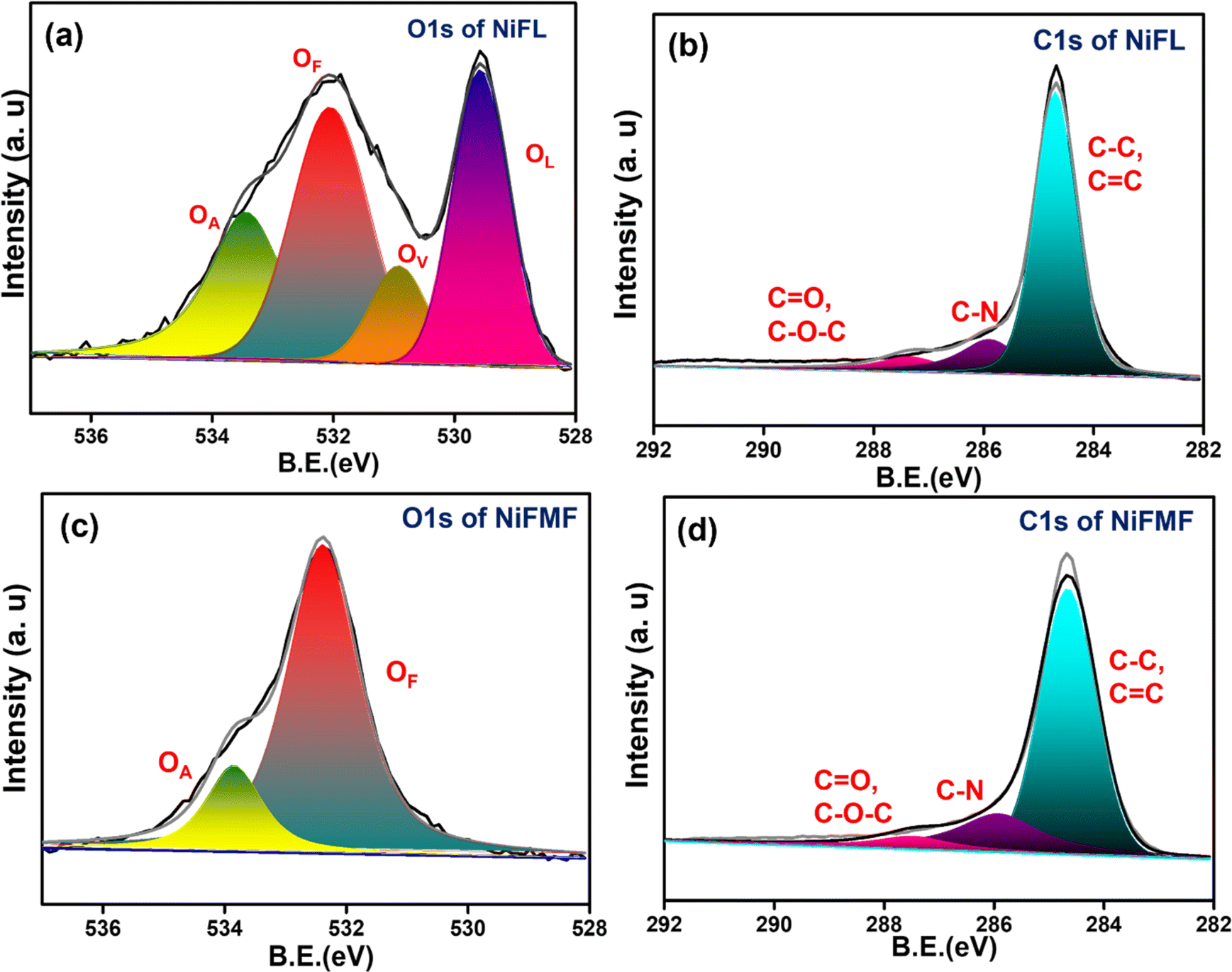
Although synthesized under identical conditions, NiFL and NiFMF differed significantly in morphological organization. Fig. 3a is the FESEM image of NiFL on a 30 μm scale. At a higher magnification, the FESEM image of NiFL showed micro ‘flower buds’ (Fig. 3b), with each layer having micro hair-like projections (Fig. 3c) with a size of approximately 50 nm. In contrast, NiFMF has two types of surfaces that can be distinguished easily by the roughness as shown in Fig. 3d. Magnified images of the smoother and rougher surfaces of NiFMF are shown in Fig. 3e and f, respectively. The rougher side shows pillar-like structures ending in spherical globules of approximately 100 nm in size, while the relatively smoother side has hair-like projections resembling the surface of the NiFL.
 | ||
| Fig. 3 FESEM images of NiFL and NiFMF. Images (a), (b) and (c) correspond to NiFL, and images (d), (e), and (f) correspond to NiFMF at comparable magnifications. Images e and f show the smoother and rougher surfaces of NiFMF, respectively. | ||
TEM images show non-uniform sized particles for both the samples. HRTEM analysis showed high-resolution lattice fringes of NiFL (Fig. 4c) having a d-spacing of 0.208, 0.203, and 0.335 nm corresponding to NiO, Ni, and graphene, respectively. The NiO layer was seen interfacing the Ni and the graphene. In contrast, the d-spacing of fringes in NiFMF (Fig. 4e) consisted of 0.203 and 0.335 nm, corresponding to Ni and graphene, respectively. The SAED pattern appeared to be of well-crystallized NiO and metallic nickel for NiFL and NiFMF, respectively. The rings were indexed to (111), (200), and (220) of NiO in NiFL (Fig. 4d) and (111) and (200) of Ni in NiFMF (Fig. 4f). The structure as deduced in the spectroscopic and diffraction studies (Fig. 1b–d) was consistent with the microscopic (TEM and HRTEM) studies (Fig. 4).
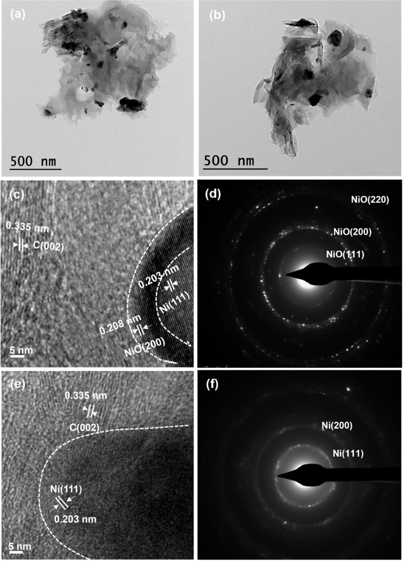 | ||
| Fig. 4 TEM image of NiFL (a) and NiFMF (b). HRTEM images and SAED patterns of NiFL ((c) and (d), respectively) and NiFMF ((e) and (f), respectively). | ||
The elemental distributions of both samples and their TEM images are shown in Fig. 5a–j. Unlike XPS, the elemental information under TEM comes from greater depths from the surface due to deeper penetration of the electron beam. In NiFL, signals due to oxygen and nickel are co-located. The localized signal indicated that O is present as oxide ions (NiO). As seen in Fig. 5c, the localization of Ni and O is stronger in NiFL, supporting the observation that the O is due to NiO. On the other hand, the O signal in NiFMF is randomly distributed. The dispersion of elements O, C, and N is uniform across the samples in NiFMF, suggesting their origin from the functionalization of the graphene matrix. Also, the N signal appeared stronger for NiFMF than NiFL, which is not expected considering the higher nitrogen-to-carbon ratio in L than M. But apart from the ratio, other factors like the solubility of ligands in benzene, the fraction of ligands in the vapor phase, and the decomposition rate of these compounds over nickel contribute to the spatial variation of N-doping in the core–shell structure.
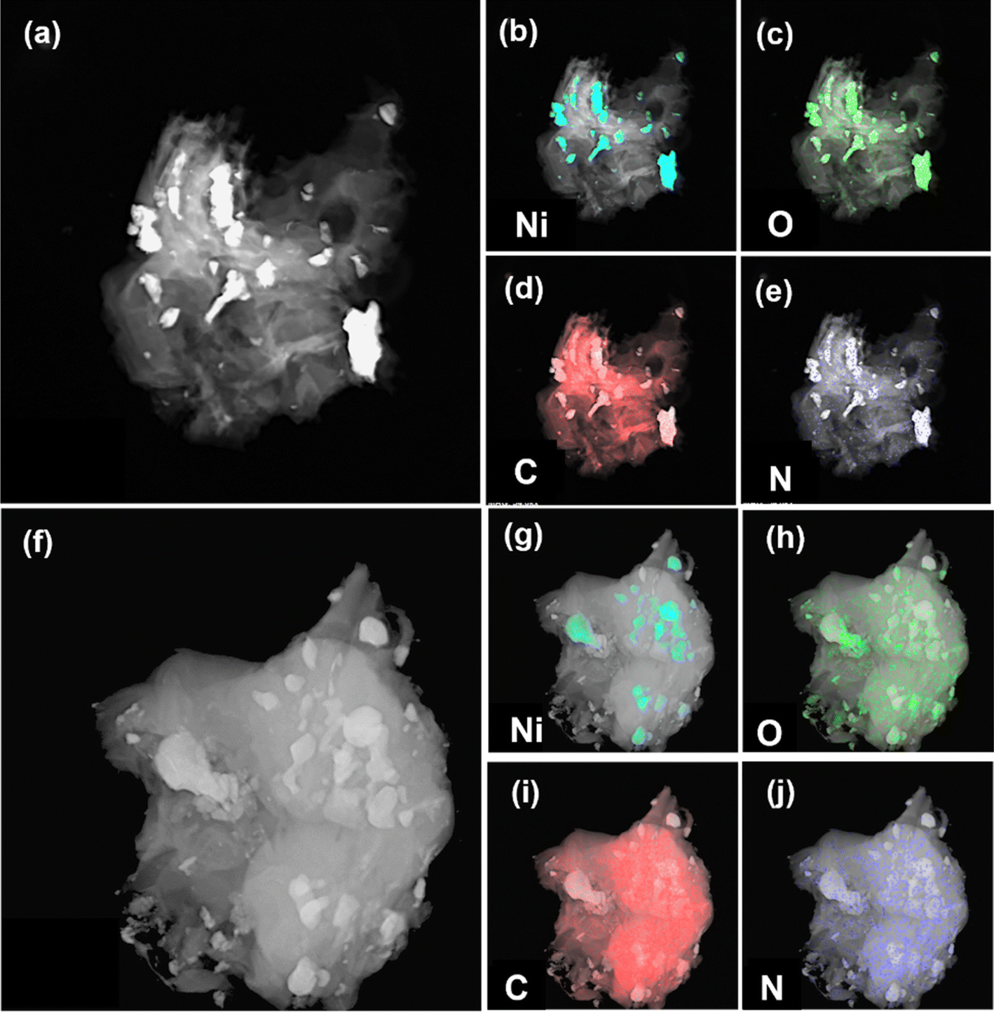 | ||
| Fig. 5 TEM image and elemental distribution of NiFL (a–e) and NiFMF (f–j). The signals corresponding to the elements are light blue (Ni), green (O), red (C), and dark blue (N). | ||
The interaction between Ni and graphene can be confirmed from the spectrum. From the Raman spectrum, the absence of the 2D band of graphene is conspicuous in NiFMF as compared to NiFL. It has been shown that a strong interaction between Ni 3d and C 2p states modifies the graphene's Dirac cone near the Fermi level which in turn alters the resonant condition of Raman scattering.34 The vanishing of the 2D band can be taken as evidence for strong electronic interaction between metallic nickel and graphene. Interestingly, a strong 2D band is seen in the Raman spectrum of NiFL, where metallic Ni and graphene are separated by NiO supporting our conclusion.
After understanding the difference in the structures of NiFL and NiFMF, both were subjected to electrochemical studies. The LSV measurements of all electrodes are depicted in Fig. 6a. Interestingly, NiFL shows a sharp increase in current density as compared to NiFMF. Moreover, the discernible peak at 1.46 V vs. RHE in NiFL can be attributed to the reduction of NiO. Correspondingly, the CV measurements within a voltage window of 1.0–1.7 V versus RHE mirror the same peak at 1.46 V versus RHE, confirming the reversible redox reaction of NiO within NiFL (Fig. S1(a)†). The electrocatalyst NiFL exhibited a superior OER performance compared to NiFMF. The overpotential values at 10 mA cm−2 for NiFL and NiFMF were 292 mV and 390 mV, respectively. The Tafel plot derived from the LSV recorded at 5 mV s−1 and linearly fitted to study the efficiency of electrocatalysts over time (Fig. 6b) revealed a Tafel slope value for NiFL ∼56% lower (∼45 mV dec−1) than NiFMF (∼79 mV dec−1). This difference stemmed from the higher kinetic activity of the surface-active catalytic sites of NiO in NiFL indicating better OER performance.
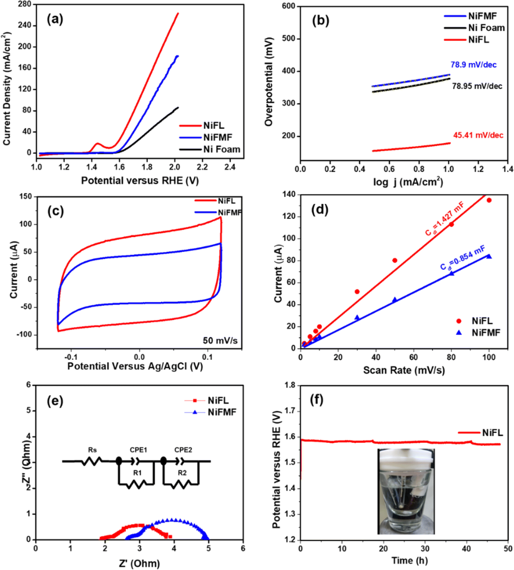 | ||
| Fig. 6 (a) Linear sweep voltammetry (LSV) curves at 5 mV s−1, (b) corresponding Tafel plot, (c) comparison of CVs for 50 mV s−1 with (d) Cdl calculation, (e) Nyquist plots of different electrocatalysts at 0.6 V versus Ag/AgCl in 1 M KOH solution, (f) chronopotentiometric stability test of NiFL at 20 mA cm−2 for 48 h. | ||
The overpotential and Tafel slope of the OER electrocatalyzed by various Ni-based catalysts are provided in Table 1. The Ni/NiO/N-doped graphene described in this work has one of the lowest overpotentials reported, suggesting the role of the microstructure. These enhancements are attributed to the well-crystalized NiO and oxygen vacancies within NiFL. The homogeneous distribution of NiO within graphitic carbon flakes in NiFL imparts greater efficiency for the OER, surpassing recently reported graphitic C/NiO electrocatalysts.54,55 The electrochemically active surface area (ECSA) is determined by performing the CVs in the non-faradaic regions from −0.12 V to +0.12 V (versus Ag/AgCl) at different scan rates ranging from 2 to 100 mV s−1 (Fig. S1(b) and (c)†). The double-layer capacitance (Cdl) values are examined to understand the active surface area responsible for OER activity. NiFL exhibited a significantly higher Cdl value (1.427 mF) than that of NiFMF (0.854 mF), as seen in Fig. 6d. While the ECSA values (ECSA = Cdl/Cs) of NiFL and NiFMF are nearly the same (0.223 cm2 and 0.211 cm2, respectively), the micro-flower bud morphology of NiFL, featuring micro-hairs on each layer of graphene flakes and uniformly distributed NiO, contributed to its superior performance over NiFMF. Turnover frequency (TOF) values for NiFL and NiFMF are 5.17 s−1 and 3.73 s−1 at 420 mV, respectively,56 highlighting the heightened kinetic reactivity of NiFL for the OER. Impedance measurements were conducted at 1.63 V (versus RHE) to measure the resistances involved during the oxygen evolution. The resulting net resistances are obtained as a sum of electrolytic resistance (Rs) and charge transfer resistance (Rct). In the case of NiFL, a lower net resistance of ∼3.4 Ω indicated faster OER (Fig. 6d). The stability of NiFL is rigorously assessed through a 48 hour chronopotentiometry test at a current density of 20 mA cm−2 (Fig. 6f). Surprisingly, a 4% reduction in the overpotential for NiFL is observed over this duration, signifying that NiFL behaves as an even better electrocatalyst with time. This high stability of NiFL may be attributed to the unique core–shell structure in Ni/NiO/graphene in contrast to polycrystalline NiFMF. Video S1† visually depicts the rigorous oxygen evolution from the NiFL electrode at 20 mA cm−2, with no significant loss of catalyst observed during oxygen evolution for 48 h, indicating the firm adhesion of the electrocatalyst onto the Ni foam substrate. The unique core–shell structure of Ni/NiO/graphene in NiFL likely contributes to its superior electrocatalytic performance with intrinsic carbon and oxygen defects, further enhancing the activity of graphitic carbon with heteroatom defects.30 As the OER has been shown to proceed via the Mars–van Krevelen mechanism in the literature,32 oxygen vacancies created due to the Ni/NiO interface and functionalized oxygen groups in the material are shown to play a crucial role in enhancing the oxygen evolution reaction on NiFL.
| Sl no. | Material | Overpotential @ 10 mA cm−2 (mV) | Tafel slope (mV dec−1) | Reference |
|---|---|---|---|---|
| 1 | NiO supported on NF | 310 | 54 | 48 |
| 2 | NiO nanosheets | 340 | 97 | 49 |
| 3 | Ni/NiOx | 390 | 70 | 50 |
| 4 | Ni@NiO/N–C nanowires | 390 | 100 | 51 |
| 5 | Ni/NiO/N-doped activated carbon | 346 | 70 | 52 |
| 6 | Ni–NiO@3-dimensional hierarchial porous graphene | 1640 | 55 | 53 |
| 7 | Ni/NiO/N-doped graphene | 292 | 45 | This work |
In order to understand the stability of the catalysts, the LSV and CV measurements were carried out for the fresh sample and after 48 h (Fig. S2†). The electrode was found to be highly stable even after 48 h of testing based on the redox peaks. A slight improvement in the performance was noticeable, probably due to improvement in the wettability of the electrode. The XPS of Ni 2p and O 1s of NiFL before reaction (a and c) and after cycling tests (b and d) are provided in Fig. S3.† The deconvoluted Ni 2p spectrum of NiFL (before reaction) showed peaks corresponding to Ni(OH)2 and Ni2+ (NiO). However, Ni(OH)2 could not be detected in the XRD, probably due to its existence confined to a few atomic layers along the surface. The deconvoluted peaks could be identified at B.E. values of 854.13 eV, 856.03 eV, 858.18 eV, 861.59 eV, 872.13 eV, 873.67 eV, 876.38 eV, and 880.38 eV corresponding to Ni2+ 2p3/2, Ni(OH)2 satellite, of Ni(OH)2 satellite, of Ni2+ 2p3/2, Ni2+ 2p1/2, Ni(OH)2 satellite, of Ni2+ 2p1/2, and satellite of Ni(OH)2, respectively. Table S1 provided in the ESI† lists the peak positions of these peaks for similar composites reported in the literature.51–53,57,58 It confirms that a shift towards higher binding energies is commonly reported in the position of Ni 2p peaks when interaction between Ni and N-doped carbon occurs. Signals due to Ni0 could not be observed in the freshly prepared NiFL probably due to its presence at deeper levels. After carrying out 100 cycles of testing, the Ni 2p spectrum showed peaks corresponding to Ni0 in addition to Ni2+ (NiO) and Ni(OH)2 suggesting partial migration of Ni0 from the core to the surface. The B.E. peaks could be indexed to 852.27 (Ni0), 854.28 (Ni2+ 2p3/2), 856.23 (Ni(OH)2), 859.25 (sat Ni0), 861.74 (sat Ni2+ 2p3/2), 864.24 (sat Ni(OH)2), 867 (Ni0), 873.63 (Ni2+ 2p1/2), 878.82 (shakeup of β-Ni(OH)2), 880.62 (shakeup of α-Ni(OH)2) and 882.2 (sat. Ni2+ 2p1/2).57,59 The O 1s spectra also showed a small shift to the higher binding energy region after the cycling tests. The migration of Ni0 to the surface is also corroborated by the decrease in the intensity of the OL and increase in the intensity of OV.
4. Conclusion
Ni/NiO encapsulated with N-doped graphene (NiFL) and Ni encapsulated with N-doped graphene (NiFMF) were synthesized using a facile and scalable ligand-assisted CVD method. The method made it convenient to control the microstructure of the nanocomposite by changing the nature as well as the concentration of the ligands. Using two types of ligands (L and M) in the L-CVD N-doped graphene on Ni or Ni/NiO was obtained. The structure-sensitivity of the NiFL and NiFMF in the OER was studied. Ni/NiO/N-doped graphene (NiFL) was a superior electrocatalyst with an overpotential of 292 mV at 10 mA cm−2 and a Tafel slope of 45.41 mV dec−1, comparable to noble metal catalysts. On the other hand, Ni/N-doped graphene (NiFMF) showed relatively lower electrocatalytic performance. The unique microstructure and compositional difference created using the ligand-assisted CVD method resulted in significantly different electrocatalytic activity in the OER.Conflicts of interest
The authors declare no conflicts of interest.Acknowledgements
Author RM would like to thank the Ministry of Education, Govt of India for an HTRA fellowship. DJ would like to acknowledge the funding from SERB (CRG/2019/001384). RG thanks SERB Women Excellence Award WEA/2020/000038 for financial support. We would also like to thank Mr Himanshu Nath for his help in the sample preparation and Dr Gaurav Bahuguna for useful discussion.References
- W. Song, Z. Ren, S. Chen, Y. Meng, S. Biswas, P. Nandi, H. A. Elsen, P. Gao and S. L. Suib, ACS Appl. Mater. Interfaces, 2016, 8, 20802, DOI:10.1021/acsami.6b06103.
- L. Yuan, Z. Yan, L. Jiang, E. Wang, S. Wang and G. Sun, J. Energy Chem., 2016, 25, 5805, DOI:10.1016/j.jechem.2016.04.013.
- J. S. Chen, J. Ren, M. Shalom, T. Fellinger and M. Antonietti, ACS Appl. Mater. Interfaces, 2016, 8, 5509, DOI:10.1021/acsami.5b10099.
- J. Xie, F. Wang, Y. Zhou, Y. Dong, Y. Chai and B. Dong, Nano-Micro Lett., 2024, 16, 39, DOI:10.1007/s40820-023-01253-9.
- D. Wu, W. Yuan, J. Wu, G. Jiang, X. Xu and S. Chang, New J. Chem., 2024, 48, 7895–7903, 10.1039/D4NJ00669K.
- C. X. Guo, S. Chen and X. Lu, Nanoscale, 2014, 6, 10896, 10.1039/C4NR03822C.
- M. Huynh, C. Shi, S. J. L. Billinge and D. G. Nocera, J. Am. Chem. Soc., 2015, 137, 14887, DOI:10.1021/jacs.5b06382.
- Y. F. Joya, H. Khalil, F. Hussain and K. S. Joya, Int. J. Hydrogen Energy, 2021, 46, 7885, DOI:10.1016/j.ijhydene.2020.11.271.
- X. Liu, H. Jia, Z. Sun, H. Chen, P. Xu and P. Du, Electrochem. Commun., 2014, 46, 1, DOI:10.1016/j.elecom.2014.05.029.
- X. Liu, S. Cui, Z. Sun and P. Du, Electrochim. Acta, 2015, 160, 202, DOI:10.1016/j.electacta.2015.01.123.
- P. W. Menezes, A. Indra, A. Bergmann, P. Chernev, C. Walter, H. Dau, P. Strasser and M. Driess, J. Mater. Chem. A, 2016, 4, 10014, 10.1039/C6TA03644A.
- D. He, X. Song, W. Li, C. Tang, J. Liu, Z. Ke, C. Jiang and X. Xiao, Angew. Chem., Int. Ed., 2020, 59, 6929, DOI:10.1002/anie.202001681.
- I. A. Buliyaminu, M. A. Aziz, S. S. Shah and Z. H. Yamani, J. Mater. Sci.: Mater. Electron., 2022, 33, 1337, DOI:10.1007/s10854-021-07452-7.
- Y.-N. Zhou, F.-T. Li, B. Dong and Y.-M. Chai, Double self-reinforced coordination modulation constructing stable Ni 4+ for water oxidation, Energy Environ. Sci., 2024, 17, 1468–1481, 10.1039/D3EE02627B.
- H. J. Liu, R. N. Luan, L. Y. Li, R. Q. Lv, Y. M. Chai and B. Dong, Chem. Eng. J., 2023, 461, 141714, DOI:10.1016/j.cej.2023.141714.
- R. D. L. Smith, M. S. Prévot, R. D. Fagan, S. Trudel and C. P. Berlinguette, J. Am. Chem. Soc., 2013, 135, 11580, DOI:10.1021/ja403102j.
- Y. Qiu, L. Xin and W. Li, Langmuir, 2014, 30, 7893, DOI:10.1021/la501246e.
- M. Shao, J. Han, W. Shi, M. Wei and X. Duan, Electrochem. Commun., 2010, 12, 1077, DOI:10.1016/j.elecom.2010.05.031.
- X. Yu, M. Zhang, W. Yuan and G. Shi, J. Mater. Chem. A, 2015, 3, 6921, 10.1039/C5TA01034A.
- S. G. Hwang, G. O. Kim, S. R. Yun and K. S. Ryu, Electrochim. Acta, 2012, 78, 406, DOI:10.1016/j.electacta.2012.06.031.
- Y. R. Ren, H. M. Wei, X. B. Huang, B. Yang, J. W. Wang and J. N. Ding, Int. J. Electrochem. Sci., 2014, 9, 7206, DOI:10.1016/S1452-3981(23)10960-6.
- T. Y. Ma, S. Dai, M. Jaroniec and S. Z. Qiao, J. Am. Chem. Soc., 2014, 136, 13925, DOI:10.1021/ja5082553.
- A. Zhao, J. Masa, W. Xia, A. Maljusch, M. Willinger, G. Clavel, K. Xie, R. Schlögl, W. Schuhmann and M. Muhler, J. Am. Chem. Soc., 2014, 136, 7551, DOI:10.1021/ja502532y.
- G. Tian, M. Zhao, D. Yu, X. Kong, J. Huang, Q. Zhang and F. Wei, Small, 2014, 10, 2251, DOI:10.1002/smll.201303715.
- X. Lu, H. M. Chan, C. Sun, C. Tseng and C. Zhao, J. Mater. Chem. A, 2015, 3, 13371, 10.1039/C5TA02967H.
- M. Zhao, X. Li, L. Song, D. He and Z. Zhang, ChemCatChem, 2016, 8, 2808, DOI:10.1002/cctc.201600562.
- J. Sun, H. Yin, P. Liu, Y. Wang, X. Yao, Z. Tang and H. Zhao, Chem. Sci., 2016, 7, 5640, 10.1039/C6SC02083F.
- Y. Wang and Y. Xia, Electrochim. Acta, 2006, 51, 3223, DOI:10.1002/asia.202001031.
- Y. Feng, H. Zhang, W. Li, L. Fang and Y. Wang, J. Power Sources, 2016, 301, 78, DOI:10.1016/j.jpowsour.2015.09.101.
- F. Dong, M. Wu, G. Zhang, X. Liu, D. Rawach, A. C. Tavares and S. Sun, Chem.–Asian J., 2020, 15, 3737, DOI:10.1002/asia.202001031.
- J. Wang, Z. Zhao, C. Shen, H. Liu, X. Pang, M. Gao, J. Mu, F. Cao and G. Li, Catal. Sci. Technol., 2021, 11, 2480, 10.1039/D0CY02333G.
- J. F. Araújo, F. Dionigi, T. Merzdorf, H. Oh and P. Strasser, Angew. Chem., Int. Ed., 2021, 60, 14981, DOI:10.1016/j.electacta.2005.09.013.
- A. R. Puigdollers, P. Schlexer, S. Tosoni and G. Pacchioni, ACS Catal., 2017, 7, 6493, DOI:10.1016/j.jpowsour.2015.09.101.
- D. Y. Usachov, V. Y. Davydov, V. S. Levitskii, V. O. Shevelev, D. Marchenko, B. V. Senkovskiy, O. Y. Vilkov, A. G. Rybkin, L. V. Yashina, E. V. Chulkov, I. Y. Sklyadneva, R. Heid, K. Bohnen, C. Laubschat and D. V. Vyalikh, ACS Nano, 2017, 11, 6336, DOI:10.1021/acsnano.7b02686.
- S. Bae, H. Kim, Y. Lee, X. Xu, J. Park, Y. Zheng, J. Balakrishnan, T. Lei, H. R. Kim, Y. I. Song, Y. Kim, K. S. Kim, B. Özyilmaz, J. Ahn, B. H. Hong and S. Iijima, Nat. Nanotechnol., 2010, 5, 574, DOI:10.1038/nnano.2010.132.
- X. Li, Y. Zhu, W. Cai, M. Borysiak, B. Han, D. Chen, R. D. Piner, L. Colombo and R. S. Ruoff, Nano Lett., 2009, 9, 4359, DOI:10.1021/nl902623y.
- A. Dahal and M. Batzill, Nanoscale, 2014, 6, 2548, 10.1039/C3NR05279F.
- A. Grüneis and D. V. Vyalikh, Phys. Rev. B: Condens. Matter Mater. Phys., 2008, 77, 193401, DOI:10.1103/PhysRevB.77.193401.
- O. Vilkov, A. Fedorov, D. Usachov, L. V. Yashina, A. V. Generalov, K. Borygina, N. I. Verbitskiy, A. Grüneis and D. V. Vyalikh, Sci. Rep., 2013, 3, 2168, DOI:10.1038/srep02168.
- J. Plutnar, M. Pumera and Z. Sofer, J. Mater. Chem. C, 2018, 6, 6082, 10.1039/C8TC00463C.
- H. Wang, T. Maiyalagan and X. Wang, ACS Catal., 2012, 2, 781, DOI:10.1021/cs200652y.
- D. Y. Usachov, V. Y. Davydov, V. S. Levitskii, V. O. Shevelev, D. Marchenko, B. V. Senkovskiy, O. Y. Vilkov, A. G. Rybkin, L. V. Yashina, E. V. Chulkov, I. Y. Sklyadneva, R. Heid, K. Bohnen, C. Laubschat and D. V. Vyalikh, ACS Nano, 2017, 11, 6336, DOI:10.1021/acsnano.7b02686.
- A. Kaniyoor and S. Ramaprabhu, AIP Adv., 2012, 2, 032183, DOI:10.1063/1.4756995.
- V. Ţucureanu, A. Matei and A. M. Avram, Crit. Rev. Anal. Chem., 2016, 46, 502, DOI:10.1080/10408347.2016.1157013.
- J. Dupin, D. Gonbeau, P. Vinatier and A. Levasseur, Phys. Chem. Chem. Phys., 2000, 2, 1319, 10.1039/A908800H.
- Z. Liu, Z. Zhao, Y. Wang, S. Dou, D. Yan, D. Liu, Z. Xia and S. Wang, Adv. Mater., 2017, 29, 1606207, DOI:10.1002/adma.201606207.
- J. Chen, X. Wu, Y. Liu, Y. Gong, P. Wang, W. Li, S. Mo, Q. Tan and Y. Chen, Appl. Surf. Sci., 2017, 425, 461, DOI:10.1016/j.apsusc.2017.06.285.
- P. T. Babar, A. C. Lokhande, M. G. Gang, B. S. Pawar, S. M. Pawar and J. H. Kim, J. Ind. Eng. Chem., 2018, 60, 493, DOI:10.1016/j.jiec.2017.11.037.
- D. Jia, H. Gao, L. Xing, X. Chen, W. Dong, X. Huang and G. Wang, Inorg. Chem., 2019, 58, 6758, DOI:10.1021/acs.inorgchem.9b00162.
- G.-Q. Han, Y.-R. Liu, W.-H. Hu, B. Dong, X. Li, X. Shang, Y.-M. Chai, Y.-Q. Liu and C.-G. Liu, Appl. Surf. Sci., 2015, 359, 172, DOI:10.1016/j.apsusc.2015.10.097.
- A. Xie, J. Zhang, X. Tao, J. Zhang, B. Wei, W. Peng, Y. Tao and S. Luo, Electrochim. Acta, 2019, 324, 134814, DOI:10.1016/j.electacta.2019.134814.
- K. N. Dinh and V. G. Gomes, Carbon, 2020, 157, 515, DOI:10.1016/j.carbon.2019.09.080.
- N. Ullah, W. T. Zhao, X. Q. Lu, C. J. Oluigbo, S. A. Shah, M. M. Zhang, J. M. Xie and Y. Xu, Electrochim. Acta, 2019, 298, 163, DOI:10.1016/j.electacta.2018.12.053.
- A. Q. Mugheri, A. Tahira, U. Aftab, M. I. Abro, S. R. Chaudhry, L. Amaral and Z. H. Ibupoto, RSC Adv., 2019, 9, 5701, 10.1039/C8RA10472G.
- S. G. Jo, C. Kim, S. J. Kim and J. W. Lee, Nanomaterials, 2021, 11, 3379, DOI:10.3390/nano11123379.
- P. Zhai, Y. Zhang, Y. Wu, J. Gao, B. Zhang, S. Cao, Y. Zhang, Z. Li, L. Sun and J. Hou, Nat. Commun., 2020, 11, 5462, DOI:10.1038/s41467-020-19214-w.
- M. C. Biesinger, B. P. Payne, A. P. Grosvenor, L. WM Lau, A. R. Gerson and R. St C. Smart, Appl. Surf. Sci., 2011, 257, 2717, DOI:10.1016/j.apsusc.2010.10.051.
- N. Srinivasa, J. P. Hughes, P. S. Adarakatti, C. Manjunatha, S. J. Rowley-Neale, S. Ashoka and C. E. Banks, RSC Adv., 2021, 11, 14654, 10.1039/D0RA10597J.
- A. N. Mansour, Surf. Sci. Spectra, 1994, 3, 231, DOI:10.1116/1.1247751.
Footnote |
| † Electronic supplementary information (ESI) available. See DOI: https://doi.org/10.1039/d4na00141a |
| This journal is © The Royal Society of Chemistry 2024 |