
 Open Access Article
 This Open Access Article is licensed under a Creative Commons Attribution-Non Commercial 3.0 Unported Licence
The AlN lattice-polarity inversion in a high-temperature-annealed c-oriented AlN/sapphire originated from the diffusion of Al and O atoms from sapphire
Ke
Jiang
ab,
Jianwei
Ben
ab,
Xiaojuan
Sun
 *ab,
Zhiming
Shi
ab,
Xianjun
Wang
ab,
Tong
Fang
ab,
Shanli
Zhang
ab,
Shunpeng
Lv
ab,
Yang
Chen
ab,
Yuping
Jia
ab,
Hang
Zang
ab,
Mingrui
Liu
ab and
Dabing
Li
*ab
*ab,
Zhiming
Shi
ab,
Xianjun
Wang
ab,
Tong
Fang
ab,
Shanli
Zhang
ab,
Shunpeng
Lv
ab,
Yang
Chen
ab,
Yuping
Jia
ab,
Hang
Zang
ab,
Mingrui
Liu
ab and
Dabing
Li
*ab
aState Key Laboratory of Luminescence and Applications, Changchun Institute of Optics, Fine Mechanics and Physics, Chinese Academy of Sciences, Changchun, 130033, P. R. China. E-mail: sunxj@ciomp.ac.cn; lidb@ciomp.ac.cn
bCenter of Materials Science and Optoelectronics Engineering, University of Chinese Academy of Sciences, Beijing, 100049, P. R. China
First published on 20th November 2023
Abstract
AlN films are widely used owing to their superior characteristics, including an ultra-wide bandgap, high breakdown field, and radiation resistance. High-temperature annealing (HTA) makes it easy to obtain high-quality AlN films, with the advantages of a simple process, good repeatability, and low cost. However, it is always found that there is a lattice-polarity inversion from a N-polarity near the sapphire to an Al-polarity in the HTA c-oriented AlN/sapphire. Currently, the formation mechanism is still unclear, which hinders its further wide applications. Therefore, the formation mechanism of the polarity inversion and its impacts on the quality and stress profile of the upper AlN in the HTA c-oriented AlN/sapphire were investigated. The results imply that the inversion originated from the diffusion of the Al and O atoms from the sapphire. Due to the presence of abundant Al vacancies (VAl) in the upper AlN, Al atoms in the sapphire diffuse into the upper AlN during the annealing to fill the VAl, resulting in the O-terminated sapphire, leading to the N-polar AlN. Meanwhile, O atoms in the sapphire also diffuse into the upper AlN during the annealing, forming an AlxOyNz layer and causing the inversion from N- to Al-polarity. The inversion has insignificant impacts on the quality and stress distribution of the upper AlN. Besides, this study predicts the presence of a two-dimensional electron gas at the inversion interface. However, the measured electron concentration is much lower than that predicted, which may be due to the defect compensation, low polarization level, and strong impurity scattering.
Introduction
AlN films are widely used in the deep ultraviolet (DUV) optoelectronic, power electronic, and surface acoustic wave devices owing to their superior characteristics, such as a direct ultra-wide band-gap, high voltage resistance, and radiation resistance, and have an important value in many fields, such as DUV disinfection and sterilization, biosensors, missile warning, solar-blind UV communication, fire monitoring, power conversion, and wave filtering.1–4 Owing to the extremely expensive nature of AlN single crystal substrates, AlN films are typically heteroepitaxially grown on substrates, such as sapphire or Si, with inevitably existing lattice and thermal mismatches, resulting in a high-density dislocation.5–8 In order to reduce the dislocation density of heteroepitaxial AlN films, researchers have developed a series of methods, such as two-step growth, insertion layer, NH3 pulse, migration enhanced epitaxy (MEE), epitaxial lateral overgrowth (ELOG), patterned or nano-patterned sapphire substrate (PSS or NPSS), and high-temperature annealing (HTA) methods, thus drawing on the experience of GaN heteroepitaxy.9–16 Among them, HTA can easily obtain high-quality AlN films and further has the advantages of a simple process, good repeatability, and low cost, thus becoming a promising method for preparing AlN films that can be widely applied in industries.17–20 For example, at present, high-quality c-oriented AlN films on sapphire substrates prepared by the HTA method have played an important role in promoting the performance of DUV light-emitting diodes.21–25The method of fabricating high-quality c-oriented AlN/sapphire by HAT was first reported by H. Miyake et al., subsequently followed by researchers all over the world.16,18,20,25 The c-oriented AlN/sapphire for annealing can be obtained by metal–organic chemical vapor deposition (MOCVD), hydride vapor phase epitaxy (HVPE), or sputtering.16–27 However, it is found that no matter what the method is, a polarity inversion from N- to Al-polarity will occur in the annealed AlN layer approximately ten to tens of nanometers above the AlN/sapphire interface.16–20,27–30 H. Miyake et al. attributed the inversion to the stress relaxation of the AlN on the sapphire substrate during sputtering and the O impurities diffusion. They believed that the lattice relaxation critical thickness of the sputtered AlN was where the inversion occurred.16,17,19,30 During the HTA process of the sputtered c-oriented AlN/sapphire, Z. B. Liu et al.31 observed that as the O2 flow increases during the sputtering, the upper AlN layer gradually transitions from pure N-polarity to pure Al-polarity with high O2 injection, indicating the important role of O impurities in the inversion process. However, some studies have also found that the epitaxial AlN on the c-sapphire substrate also exhibits the polarity inversion phenomenon without intentionally introducing any additional O impurities during the growth process.32–35
Therefore, further research is needed on the mechanism of the AlN polarity inversion as well as its impact on the quality and stress of the upper AlN layer. The following questions should be answered: (1) whether the formation of the polarity inversion is related to the stress relaxation during the sputtering process? (2) What is the role of O impurities? Is the O element necessary and what O concentrations are needed? Whether other types of defects are involved during the polarity inversion process? (3) Does the polarity inversion have an impact on the dislocation and stress evolution in the upper AlN? (4) What are the merits of the polarity inversion? How to use it? In this context, we investigated the mechanism of the polarity inversion and its impact on the quality and the stress profile of the upper AlN in the HTA c-oriented AlN/sapphire. The results showed that the polarity inversion may be related not only to the O impurities but also to Al vacancies (VAl). Moreover, the appearance of the polarity inversion has little impact on the crystal quality and the stress profile. Theoretically, there will be a two-dimensional electron gas (2DEG) at the inversion interface, which may expand the application of the HTA AlN/sapphire.
Experimental
AlN films were sputtered on the c-sapphire substrates at 650 °C in an N2 atmosphere with a chamber pressure of 4 mTorr. The sputtered templates were annealed at 1750 °C for 1 hour using a face-to-face geometry in an N2 atmosphere, as shown in Fig. 1a. To confirm the lattice changes of the c-oriented AlN/sapphire before and after annealing, the magnetron sputtered samples with and without annealing were studied using the aberration-corrected scanning transmission electron microscopy (AC-STEM) with the high-resolution (HR) high-angle annular dark field (HAADF) mode. At the same time, the element distributions of the AlN/sapphire after annealing were analyzed by electron energy loss spectroscopy (EELS). STEM-ready samples were prepared by the in situ focused ion beam (FIB) lift-out technique on an FEI dual beam FIB/SEM. The samples were capped with sputtered C and e-Pt/I-Pt prior to milling. The STEM lamella was about 100 nm. The samples were imaged using an FEI Tecnai TF-20 FEG/TEM at 200 kV in the HAADF mode. The STEM probe size was 1–2 nm in the nominal diameter. EELS mappings were acquired on an Oxford INCA Bruker Quantax EELS system.36 The atomic arrangement and stress distributions were studied by analyzing the STEM images by Fourier transform, inverse Fourier transform, and geometric phase analysis (GPA) using the digital micrograph software.37 Photoluminescence (PL) measurements were applied to analyze the defects of the c-oriented AlN/sapphire before and after annealing at room temperature (RT). The excitation wavelength of the laser was 213 nm and the light power was 20 mW. Van der Pauw Hall measurements were used to confirm the existence of the polarization-induced 2EDG at RT at the inversion interface in the HTA AlN/sapphire. The samples were prepared by photolithography, exposing the inversion interface via inductively coupled plasma etching, Ti/Al/Ni/Au deposition by electron beam evaporation, lift-off, and rapid thermal annealing. | ||
| Fig. 1 (a) A schematic diagram of the face-to-face HTA of the sputtered AlN/sapphire; (b) the cross-sectional HAADF STEM image of the HTA c-oriented AlN/sapphire; (c) the cross-sectional HR HAADF STEM image near the HTA c-oriented AlN/sapphire interface; (d) an enlarged image of the white box in (c); (e and f) enlarged images of the white boxes in (d); (g and h) schematic diagrams of the atomic arrangement of (e and f). The STEM images are along the AlN 〈11−20〉 direction. | ||
The first-principle calculations and numerical simulations were employed to confirm the effects of O impurity on the polarity inversion and to predict the polarization-induced electron concentration. The first-principle calculations were performed based on the density functional theory (DFT) methods, as implemented in the VASP package.38 The projector-augmented wave (PAW) method for the core region and the Perdew–Burke–Ernzerhof (PBE) for the exchange-correlation potential of the valence electrons were employed.39,40 A kinetic energy cutoff of 400 eV was chosen. The supercell was used to minimize the in-plane lattice mismatch. The 2 × 2 × 1 supercell for sapphires and 3 × 3 × 1 supercell for 4-layer AlN slabs were used to ensure that the in-plane lattice mismatch was smaller than 2%. The vacuum layer was set to be larger than 10 Å to avoid the imaginary interaction. The bottom three-atomic layer was fixed during all structural relaxations. The k-mesh was set to 0.04 2π Å−1, and the maximum force on each atom was less than 0.01 eV Å−1 in the structural relaxation. The commercial APSYS software was used in the numerical simulations. The simulations were conducted by self-consistently solving Poisson's equation, continuity equation, and drift-diffusion equation with proper boundary conditions. The polarization level was set to 60%, and the background electron concentration for AlN was set to 1012 cm−3.
Results and discussion
Through the HADDF STEM image, as shown in Fig. 1b, it can be clearly seen that there is a black line above the interface between the sapphire substrate and the upper AlN layer, almost parallel to the interface between the AlN layer and the sapphire substrate. This phenomenon can commonly be observed in the HTA c-oriented AlN/sapphire when the annealing temperature and annealing time reach certain conditions (generally more than one hour and higher than 1500 °C).16–20,28–30 The HR HADDF STEM image near the interface between the AlN and the sapphire, as shown in Fig. 1c, shows that the black contrast line area was approximately 10 nm away from the AlN/sapphire interface, and its own thickness was about 1–2 nm. The black contrast line area has approximately 5–6 atomic layers along the 〈0001〉 direction, and the arrangement of the atoms exhibits certain irregular characteristics, as shown in Fig. 1d. Besides, the atoms on both sides of the black contrast line area exhibit regular arrangement but show different orientations. Above the black contrast line, lattice arrangement analysis shows that it is Al-polarity, as shown in Fig. 1e and g, while below the black contrast line, lattice arrangement analysis shows it has N-polarity, as shown in Fig. 1f and h. Therefore, the black contrast line is a polarity inversion interface, from an N- to an Al-polarity along the 〈0001〉 direction.To analyze whether the observed polarity inversion is related to the critical thickness of the lattice relaxation between the AlN layer and the sapphire substrates, the HADDF STEM image of an unannealed magnetron sputtered AlN/sapphire is also captured, as shown in Fig. 2a. It can be seen that the unannealed AlN has a polycrystalline structure with a large number of grain boundaries. However, in the AlN layer, within the range from over ten to tens of nanometers above the sapphire surface, where the polarity inversion occurs after annealing, no obvious dual-layer caused by strain relaxation is directly observed, indicating that the lattice relaxation may not have occurred significantly. The corresponding selected area electron diffraction (SAED) image shows that although the unannealed AlN has a polycrystalline structure, it still has a c-preferred orientation, as shown in Fig. 2b. The inverse Fourier transform image of the (0001) diffraction plane further proves that there are a large number of extended defects at the grain boundaries, but the grain boundary defects are almost uniformly distributed throughout the AlN layer and do not exhibit a defect accumulation phenomenon near the interface between the AlN layer and the sapphire substrate. This result proves that the occurrence of the polarity inversion after HTA may not be related to the critical thickness of lattice relaxation during the sputtering.
 | ||
| Fig. 2 (a) The HAADF STEM image of the as-sputtered AlN/sapphire and (b) the corresponding SAED image. (c) The inverse Fourier transform image of the (0001) planes of (a). The STEM images are along the AlN 〈1−100〉 direction. | ||
To confirm the relationship between the polarity inversion and the extended defects, such as dislocations and stack faults, we conduct HR HADDF STEM on the interface between the AlN layer and sapphire substrate, as well as the polarity reversion interface. Fig. 3a shows the HR HADDF STEM image of the interface between the AlN layer and the sapphire substrate. There are no lattice mismatches as well as lattice-mismatch-related dislocations in the N-polar AlN. The inverse Fourier transform images of the (11−20) and (0001) planes, as shown in Fig. 3b and c, clearly show that the atoms in the N-polar AlN layer are arranged uniformly along the 〈0001〉 and 〈11−20〉 directions, without any dislocations or stacking faults. At the same time, it can also be observed that a typical 8/9 atomic arrangement structure is formed at the interface between the AlN layer and the sapphire substrate, indicating that the lattice stress is completely released through the atomic mismatch. Hence, the strong compressive stress of the substrate on the upper AlN layer should not come from the lattice mismatch, but from the thermal residual stress. Fig. 3d is the HR HADDF image of the AlN polarity inversion region, and Fig. 3e and f are the corresponding inverse Fourier transform images of the (11−20) and (0001) planes. Both, the N- and Al-polar AlN layers do not exist dislocations, and the atoms at the polarity inversion region are also regularly arranged in the 〈0001〉 and 〈11−20〉 directions. These results indicate that the polarity inversion may not originate from extended defects such as dislocations or stacking faults, and it also will not induce extended defects.
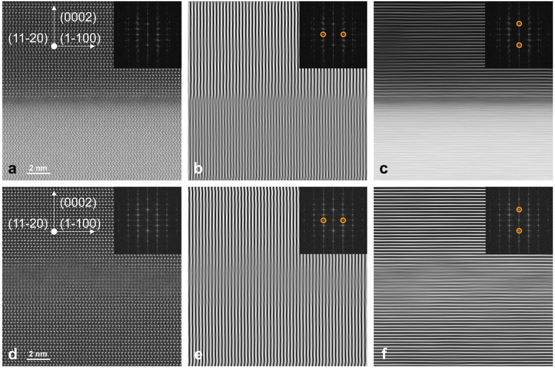 | ||
| Fig. 3 (a–c) The cross-sectional HR HAADF STEM image near the HTA AlN/sapphire interface and its corresponding inverse Fourier transform images of (11−20) and (0001) planes; (d–f) the cross-sectional HR HAADF STEM image near the polarity inversion interface and its corresponding inverse Fourier transform images of (11−20) and (0001) planes. The STEM images are along the AlN 〈11−20〉 direction. The inserts are the SAED images. | ||
Furthermore, in order to analyze the effect of the polarity inversion on the strain profile, the regions including the AlN/sapphire interface and polarity inversion interface are observed by the HADDF STEM along different directions, and their geometric phase images are analyzed. Fig. 4a–c shows the HADDF STEM image along the 〈11−20〉 direction, and its corresponding GPA images, which represent the horizontal and vertical strain distribution, exx and eyy, respectively. Obviously, the strain distribution along the horizontal and vertical directions above and below the polarity inversion interface is uniform, and just small strain oscillations can be observed at the polarity inversion interface. Fig. 4d–f shows the HADDF STEM image along the 〈1−100〉 direction, and its corresponding GPA images. From this direction, the strain oscillations of the polarity interface and its upper and lower regions are not observed. These results imply that the polarity inversion may not have a significant impact on the in-plane strain of the wafer, and also indirectly indicate that the change in polarity is likely due to the non-extended defects.
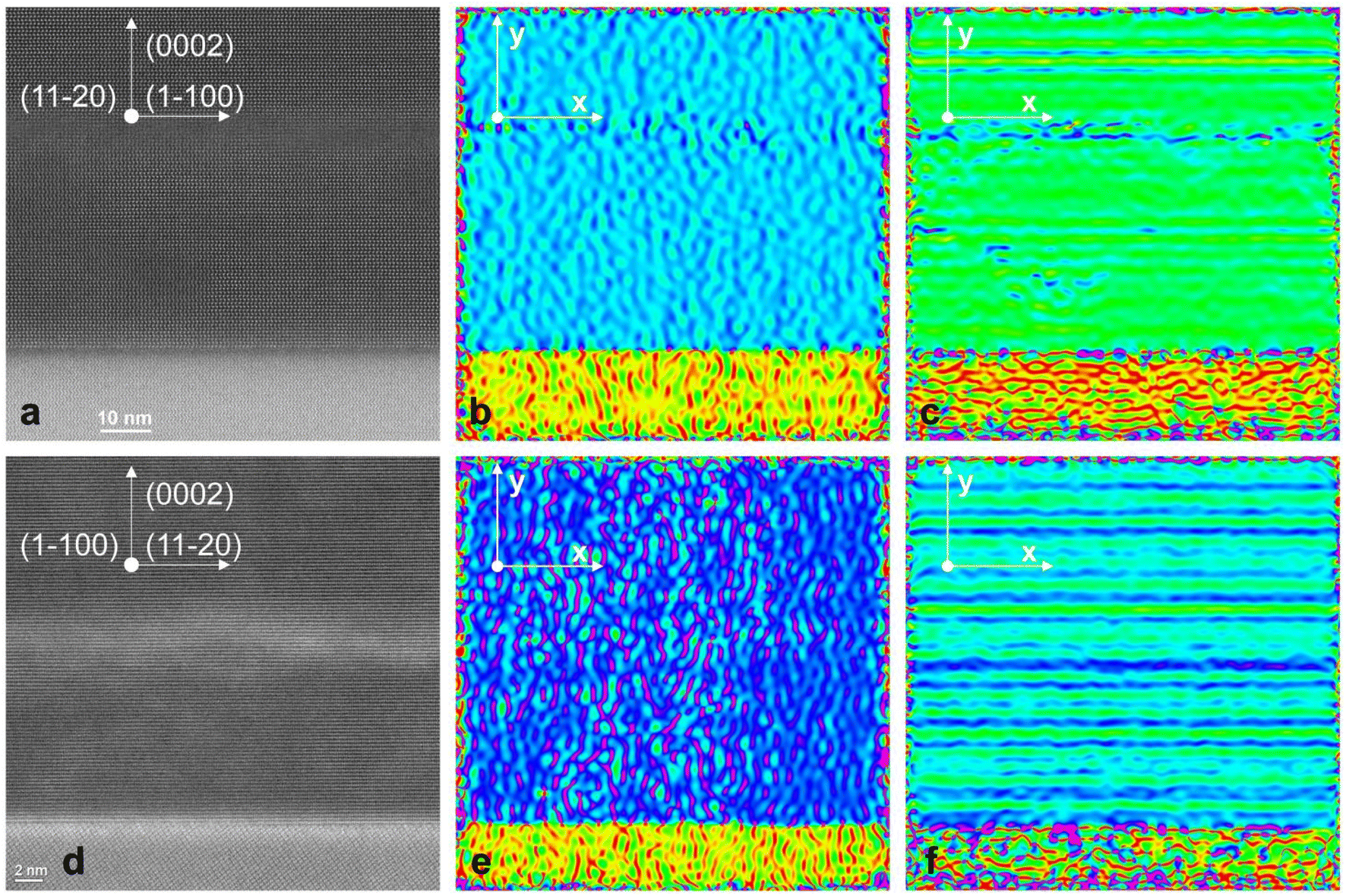 | ||
| Fig. 4 (a–c) The cross-sectional HR HAADF STEM image along the 〈11−20〉 direction of the HTA sample near the AlN/sapphire interface and the polarity inversion interface, and the in-plane strain profile exx and eyy GPA images; (d–f) cross-sectional HR HAADF STEM image along the 〈1−100〉 direction of the HTA sample near the AlN/sapphire interface and polarity inversion interface, and the in-plane strain profile exx and eyy GPA images. | ||
The PL spectrum of the HTA AlN/sapphire exhibits three emission peaks, as shown in Fig. 5a, labeled as peak-1, peak-2, and peak-3, respectively. By further conducting PL measurements on the as-sputtered AlN/sapphire and the sapphire substrate, as shown in Fig. 5b and c, it can be confirmed that the peak-3 is an emission peak related to the sapphire substrate, while the peak-1 is an emission peak that already exists before annealing. It is worth noting that several sharp emissions at approximately 230–350 nm, as shown in Fig. 5b, are originating from the PL instrument. As for peak-2, the position is located near 365 nm, corresponding to the photon energy of approximately 3.4 eV, which is a typical PL emission peak related to the VAl.41–43 Therefore, it can be confirmed that there are a large number of VAl in the AlN/sapphire after HTA. It is believed that the VAl should have been formed after magnetron sputtering, but due to its polycrystalline structure before annealing, it may not produce a significant luminescence peak.
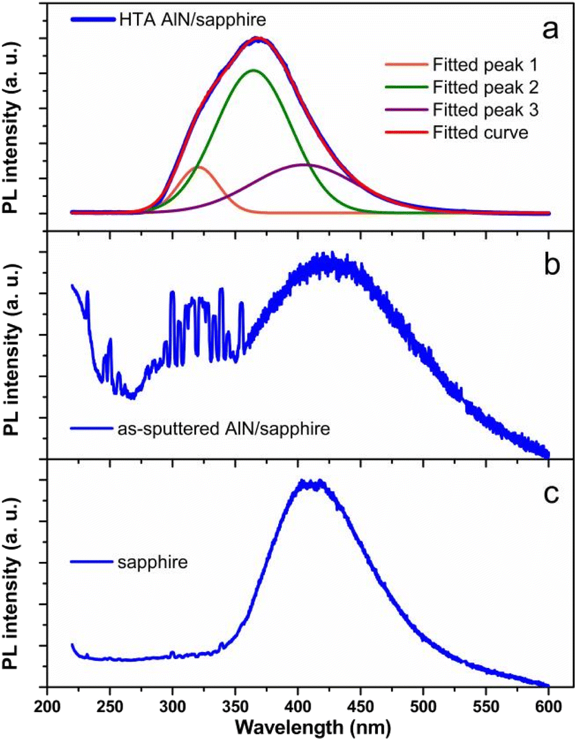 | ||
| Fig. 5 The PL spectra of (a) the HTA AlN/sapphire, (b) the as-sputtered AlN/sapphire, and (c) the sapphire substrate. | ||
We again analyze the HR HADDF STEM image of the AlN/sapphire interface of the HTA sample to verify whether VAl has an impact on the occurrence of the polarity inversion, as shown in Fig. 6a, where the bright contrast represents the Al atom with a large atomic number. There is a clear dark contrast in the sapphire near the interface (the white solid box), indicating that there may be an Al atom deficiency in this area. It can be seen more clearly, as shown in Fig. 6b, that there are indeed missing Al atoms in the sapphire near the interface, and the atomic arrangement has also been changed. This may be due to the diffusion of Al atoms in the sapphire into the magnetron-sputtered AlN at high temperatures, filling some VAl and producing an O-terminated sapphire surface. In addition, element analyses are conducted on the AlN/sapphire interface and the polarity inversion interface. As shown in Fig. 6c–f, the HADDF STEM image and the corresponding EELS mappings of Al, N, and O elements in the green box area are presented. The area near the surface of the sapphire shows a slight decrease in the Al element compared to the interior of the sapphire. At the polarity the inversion interface, Al, and N elements slightly decrease compared to other positions, while the O element slightly increases. EELS spectra at the polarity inversion interface (obtained at the position marked by the white point “P” in Fig. 6c) also clearly show the K-edge line of the O element, as shown in Fig. 6g, which also proves the existence of the O element. Therefore, we may speculate the formation process of the N-polar AlN and the polarity inversion process similar to that with the Al atoms near the interface in the sapphire substrate diffuse to the AlN layer during the HTA process and occupy VAl in the AlN layer, forming an O-terminated sapphire surface, leading to the formation of the N-polar AlN. At the same time, the O atoms also diffuse upwards to the AlN layer and enrich at a certain position, forming an AlxOyNz layer, leading to the polarity inversion.44,45
 | ||
| Fig. 6 (a) The cross-sectional HR HAADF STEM image along the 〈11−20〉 direction near the HTA AlN/sapphire interface; (b) an enlarged image of the white dashed box area in (a); (c–f) the cross-sectional HAADF STEM image along the 〈1−100〉 direction of the HTA sample near the AlN/sapphire interface and polarity inversion interface, and the corresponding EELS mappings of Al, N, and O elements; (g) EELS at the polarity inversion interface marked by the white point “P” in (c), and the insert shows the K-edge of the O element. | ||
The thermal stability of both Al- and N-polar AlN slabs on the Al- and O-terminated sapphire substrate are calculated to confirm our above analysis. Al- and N-polar AlN slabs are stacked on the Al- and O-terminated sapphire with a 2 Å interval for the initial states. After the full structural relaxation, the covalent chemical bonds are formed at the interface. On the Al-terminated sapphire, the Al-polar AlN slab exhibits lower free energy than that of the N-polar AlN slab by 2.79 eV, as shown in Fig. 7a and b. Notably, the N-polar AlN slab is converted into a quasi-hexagonal transition state after relaxation, implying the trend of a polarity inversion. The result on the O-terminated sapphire is quite different, as shown in Fig. 7c and d. The N-polar AlN slab is more stable than the Al-polar AlN slab by 1.41 eV, meanwhile, the Al-polar AlN slab relaxes to the quasi-hexagonal transition state on the O-terminated sapphire, implying that the N-polar AlN layer is energetically favorable than the Al-polar one on an O-terminated sapphire. Therefore, the formation of the N-polar AlN is quite possibly attributed to the formation of O-terminated sapphire due to the Al atoms diffusing into the upper AlN layer to occupy VAl during the annealing process, as analyzed above.
 | ||
| Fig. 7 The atomic structures of the initial and relaxed AlN slab on the sapphire and the O-terminated N-polar AlN. (a and b) Al- and N-polar AlN slabs on the Al-terminated sapphire; (c and d) Al- and N-polar AlN slabs on the O-terminated sapphire; (e and f) Al- and N-polar AlN slabs on O-terminated N-polar AlN. | ||
Furthermore, we theoretically confirmed whether the incorporation of the O atoms can be attributed to the polarity inversion. Firstly, we assum that the O atoms substitute the N sites to form an O-terminated N-polar AlN layer. Then, we artificially cover both the Al-polar and N-polar AlN slabs on the O-terminated N-polar AlN layer and perform the structural relaxation. It is found that the free energy of the Al-polar AlN slab on the O-terminated N-polar AlN layer is 2.42 eV lower than that of the N-polar AlN slab on the O-terminated N-polar AlN layer, as shown in Fig. 7e and f. However, we emphasize that the polarity of the upper AlN on the O-terminated N-polar AlN layer is related to the O atom content, as shown in Fig. 8a. With the increase of O atom content on the surface, the free energy of the Al-polar AlN slab on the O-terminated N-polar AlN layer gradually decreases while that of the N-polar AlN slab shows the opposite trend. The Al-polar AlN slab on the O-terminated N-polar AlN layer is more stable only on the condition that the O atom content is higher than 87.5%, implying that the polarity inversion requires relatively high O concentration.
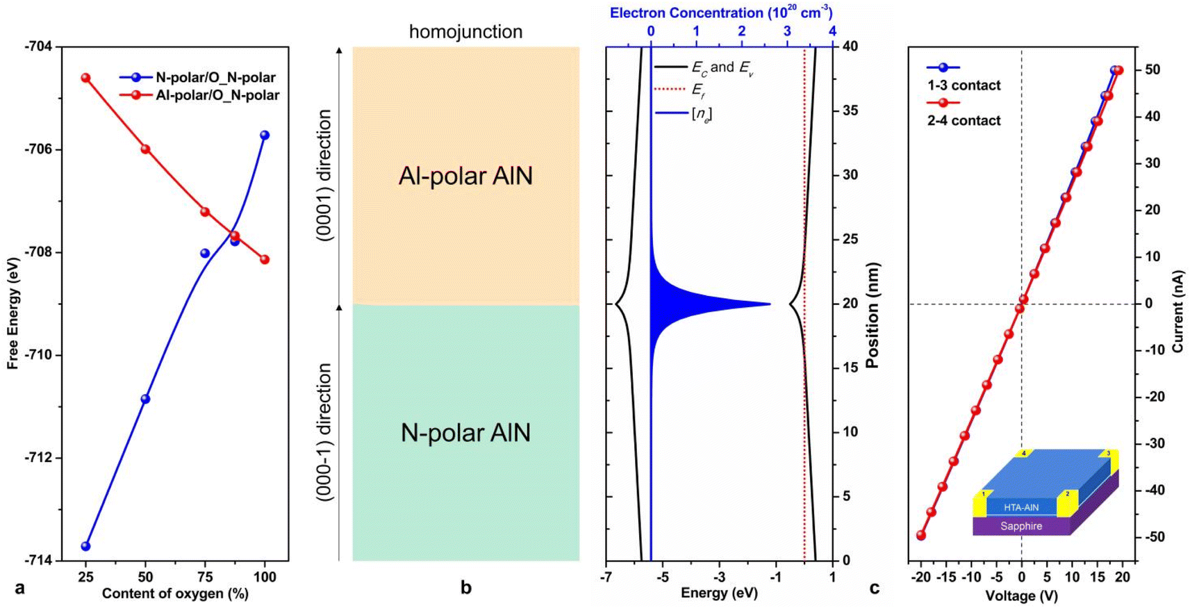 | ||
| Fig. 8 (a) The free energy of the Al- and N-polar AlN slabs on O-terminated N-polar AlN as a function of the O content by the first-principle calculation; (b) a schematic diagram of the homogeneous junction formed by a N-polar AlN layer and an Al-polar AlN layer and the corresponding numerically-simulated energy band profile and carrier distribution by APSYS; (c) IV curves between the contacts 1, 3 and 2, 4 during the Hall measurement and the insert is the schematic diagram of the measured sample. | ||
In theory, due to the spontaneous polarization effect of the AlN, there will be polarization-induced charges at the polarity inversion interface. Specifically, inversion from N- to Al-polarity will generate polarization-induced 2DEG at the interface. Firstly, we use the APSYS software to simulate the 2DEG concentration. The calculation model is the homogeneous junction formed by 20 nm N-polar AlN and 20 nm Al-polar AlN and the corresponding energy band and carrier concentration distribution are calculated, as shown in Fig. 8b. In the N-polar AlN, the energy band bends downwards along the 〈000−1〉 direction, while in the Al-polar AlN, the energy band bends upwards along the 〈0001〉 direction. At the polarity inversion interface, the conduction band is actually bent below the Fermi level, thus forming 2DEG whose concentration could reach the order of 1020 cm−3. It may have potential application in the high electron mobility transistor (HEMT) device. The van der Pauw Hall measurement is employed to measure the carrier concentration at the polarity inversion interface of the HTA AlN/sapphire. The prepared Hall measurement sample is shown as the insert in Fig. 8c. From its current–voltage (IV) curves, as shown in Fig. 8c, the electrode contacts of the Hall measurement sample exhibit good ohmic characteristics, proving that the conductivity of the HTA AlN/sapphire is better than that of the generally epitaxial AlN thin film, which may be due to 2DEG at the polarity inversion interface. The Hall measurement results show that the carrier sheet concentration is about 8.5 × 1010 cm−2. If the carriers are assumed to fully concentrate on the polarity inversion interface of 1–2 nm, the carrier concentration is about (4.25–8.5) × 1017 cm−3, and its mobility is only 0.3 cm2 V−1 s−1. We believe that the reason why the carrier concentration and mobility of the HTA sample are much lower than the theoretical values is perhaps the intense defect compensation, low polarization level, and strong impurity and interface scattering. How to improve its carrier concentration and mobility is a key problem to be solved in the future for applications.
Conclusions
In summary, it is found that there is always a lattice-polarity inversion from N- to Al-polarity in an HTA c-oriented AlN/sapphire above the interface between the AlN and sapphire, while the formation mechanism is still controversial. We, therefore, investigate the formation mechanism of the polarity inversion and its impact on the quality and stress profile of the upper AlN in the HTA c-oriented AlN/sapphire. We find that the polarity inversion may not be related to the critical thickness of the lattice relaxation during the sputtering and the extended defects, such as dislocations or stacking faults. The non-extended defects, including VAl and O impurities, may induce the polarity inversion. The Al atoms near the interface in the sapphire diffuse to the upper AlN layer during the HTA process and occupy its VAl, forming an O-terminated sapphire surface, leading to the formation of the N-polar AlN layer. Meanwhile, the O atoms in the sapphire also diffuse upwards to the AlN layer and are enriched at a certain position, forming an AlxOyNz layer, leading to the polarity inversion. We believe that this process may also explain the polarity inversion in the epitaxial AlN on the c-sapphire substrate without intentionally introducing additional O impurities. Besides, the polarity inversion has little impact on the crystal quality and the stress profile. Theoretically, the polarity inversion can induce a 2DEG with a concentration over 1020 cm−3, which may expand the future applications of the HTA c-oriented AlN/sapphire, such as the HEMT. However, the measured electron concentration and mobility are much lower than the prediction, which may originate from the intense defect compensation, low polarization level, and strong impurity and interface scattering. If the mobility and concentration of the polarity inversion-induced electron can be optimized, the application of the HTA AlN/sapphire will be further expanded.Author contributions
Ke Jiang directed the STEM and EDS measurements, processed the STEM images, performed the PL and Hall measurements, analyzed the results, and conceptualized and wrote the manuscript. Jianwei Ben and Shanli Zhang fabricated the AlN/sapphire templates and helped to analyze the results. Zhiming Shi, Hang Zang, and Xianjun Wang performed the calculations and helped to analyze the results. Tong Fang fabricated the samples for Hall measurements. Shunpeng Lv, Yang Chen, Yuping Jia, and Mingrui Liu helped to analyze the results. Xiaojuan Sun and Dabing Li guided all the experiments and analyses and revised the manuscript.Conflicts of interest
There are no conflicts to declare.Acknowledgements
National Key R&D Program of China (2022YFB3604903), National Natural Science Foundation of China (62121005, 62004196, 12234018, U22A2084), Youth Innovation Promotion Association of CAS (2023223), Natural Science Foundation of Jilin Province (20230101345JC, 20230101360JC), Young Elite Scientist Sponsorship Program by CAST (YESS20200182).Notes and references
- D. B. Li, K. Jiang, X. J. Sun and C. L. Guo, AlGaN photonics: recent advances in materials and ultraviolet devices, Adv. Opt. Photon, 2018, 10, 43–110 CrossRef.
- M. Kneissl, T.-Y. Seong, J. Han and H. Amano, The emergence and prospects of deep-ultraviolet light-emitting diode technologies, Nat. Photonics, 2019, 13, 233–244 CrossRef CAS.
- Q. Cai, H. F. You, H. Guo, J. Wang, B. Liu, Z. L. Xie, D. J. Chen, H. Lu, Y. D. Zheng and R. Zhang, Progress on AlGaN-based solar-blind ultraviolet photodetectors and focal plane arrays, Light: Sci. Appl., 2021, 10, 94 CrossRef CAS PubMed.
- A. M. Gao, K. F. Liu, J. R. Liang and T. Wu, AlN MEMS filters with extremely high bandwidth widening capability, Microsyst. Nanoeng., 2020, 6, 74 CrossRef.
- D. Y. Fu, D. Lei, Z. Li, G. Zhang, J. L. Huang, X. J. Sun, Q. K. Wang, D. B. Li, J. Wang and L. Wu, Toward Φ56 mm Al-Polar AlN Single Crystals Grown by the Homoepitaxial PVT Method, Cryst. Growth Des., 2022, 22, 3462–3470 CrossRef CAS.
- Q. Wang, D. Lei, J. L. Huang, X. J. Sun, D. B. Li, Z. X. Zhou and L. Wu, Homoepitaxial growth of 3-inch single crystalline AlN boules by the physical vapor transport process, Frontiers in Materials, 2023, 9, 1128468 CrossRef.
- H. L. Wu, K. Zhang, C. G. He, L. F. He, Q. Wang, W. Zhao and Z. T. Chen, Recent Advances in Fabricating Wurtzite AlN Film on (0001)-Plane Sapphire Substrate, Crystals, 2022, 12(1), 38 CrossRef CAS.
- J. F. Shen, X. L. Yang, D. S. Liu, Z. D. Cai, L. Wei, N. Xie, F. J. Xu, N. Tang, X. Q. Wang, W. K. Ge and B. Shen, High quality AlN film grown on a nano-concave-circle patterned Si substrate with an AlN seed layer, Appl. Phys. Lett., 2020, 117(2), 022103 CrossRef CAS.
- X. J. Sun, D. B. Li, Y. R. Chen, H. Song, H. Jiang, Z. M. Li, G. Q. Miao and Z. W. Zhang, In situ observation of two-step growth of AlN on sapphire using high-temperature metal-organic chemical vapour deposition, CrystEngComm, 2013, 15(30), 6066–6073 RSC.
- K. Jiang, X. J. Sun, J. W. Ben, Y. P. Jia, H. N. Liu, Y. Wang, Y. Wu, C. H. Kai and D. B. Li, The defect evolution in homoepitaxial AlN layers grown by high-temperature metal-organic chemical vapor deposition, CrystEngComm, 2018, 20, 2720–2728 RSC.
- J. P. Zhang, M. A. Khan, W. H. Sun, H. M. Wang, C. Q. Chen, Q. Fareed, E. Kuokstis and J. W. Yang, Pulsed atomic-layer epitaxy of ultrahigh-quality AlxGa1-xN structures for deep ultraviolet emissions below 230 nm, Appl. Phys. Lett., 2002, 81(23), 4392–4394 CrossRef CAS.
- R. G. Banal, M. Funato and Y. Kawakam, Characteristics of high Al-content AlGaN/AlN quantum wells fabricated by modified migration enhanced epitaxy, Phys. Status Solidi C, 2010, 7, 2111–2114 CrossRef CAS.
- N. Susilo, E. Ziffer, S. Hagedorn, L. Cancellara, C. Netzel, N.-L. Ploch, S. J. Wu, J. Rass, S. Walde, L. Sulmoni, M. Guttmann, T. Wernicke, M. Albrecht, M. Weyers and M. Kneissl, Improved performance of UVC-LEDs by combination of high-temperature annealing and epitaxially laterally overgrown AlN/sapphire, Photonics Res., 2020, 8, 589–594 CrossRef CAS.
- J. M. Wang, N. Xie, F. J. Xu, L. S. Zhang, J. Lang, X. N. Kang, Z. X. Qin, X. L. Yang, N. Tang, X. Q. Wang, W. K. Ge and B. Shen, Group-III nitride heteroepitaxial films approaching bulk-class quality, Nat. Mater., 2023, 22, 853–859 CrossRef CAS PubMed.
- L. S. Zhang, F. J. Xu, J. M. Wang, C. G. He, W. W. Guo, M. X. Wang, B. W. Sheng, L. Lu, Z. X. Qin, X. Q. Wang and B. Shen, High-quality AlN epitaxy on nano-patterned sapphire substrates prepared by nano-imprint lithography, Sci. Rep., 2016, 6, 35934 CrossRef CAS.
- H. Miyake, C.-H. Lin, K. Tokoro and K. Hiramatsu, Preparation of high-quality AlN on sapphire by high-temperature face-to-face annealing, J. Cryst. Growth, 2016, 456, 155–159 CrossRef CAS.
- S. Y. Xiao, R. Suzuki, H. Miyake, S. Harada and T. Ujihara, Improvement mechanism of sputtered AlN films by high-temperature annealing, J. Cryst. Growth, 2018, 502, 41–44 CrossRef CAS.
- J. W. Ben, X. J. Xun, Y. P. Jia, K. Jiang, Z. M. Shi, H. N. Liu, Y. Wang, C. H. Kai, Y. Wu and D. B. Li, Defect evolution in AlN templates on PVD-AlN/sapphire substrates by thermal annealing, CrystEngComm, 2018, 20, 4623–4629 RSC.
- S. Tanaka, K. Shojiki, K. Uesugi, Y. Hayashi and H. Miyake, Quantitative evaluation of strain relaxation in annealed sputter-deposited AlN film, J. Cryst. Growth, 2019, 512, 16–19 CrossRef CAS.
- M. X. Wang, F. J. Xu, N. Xie, Y. H. Sun, B. Y. Liu, W. K. Ge, X. N. Kang, Z. X. Qin, X. L. Yang, X. Q. Wang and B. Shen, High-temperature annealing induced evolution of strain in AlN epitaxial films grown on sapphire substrates, Appl. Phys. Lett., 2019, 114(11), 112105 CrossRef.
- N. Susilo, S. Hagedorn, D. Jaeger, H. Miyake, U. Zeimer, C. Reich, B. Neuschulz, L. Sulmoni, M. Guttmann, F. Mehnke, C. Kuhn, T. Wernicke, M. Weyers and M. Kneissl, AlGaN-based deep UV LEDs grown on sputtered and high temperature annealed AlN/sapphire, Appl. Phys. Lett., 2018, 112, 041110 CrossRef.
- M. X. Wang, F. J. Xu, J. M. Wang, N. Xie, Y. H. Sun, B. Y. Liu, J. Lang, N. Zhang, W. K. Ge, X. N. Kang, Z. X. Qin, X. L. Yang, X. Q. Wang and B. Shen, The sapphire substrate pretreatment effects on high-temperature annealed AlN templates in deep ultraviolet light emitting diodes, CrystEngComm, 2019, 21, 4632 RSC.
- R. X. Ni, C.-C. Chuo, K. Yang, Y. J. Ai, L. Zhang, Z. Cheng, Z. Liu, L. F. Jia and Y. Zhang, AlGaN-based ultraviolet light-emitting diode on high-temperature annealed sputtered AlN template, J. Alloys Compd., 2019, 794, 8–12 CrossRef CAS.
- K. Uesugi, S. Kuboya, K. Shojiki, S. Y. Xiao, T. Nakamura, M. Kubo and H. Miyake, 263 nm wavelength UVC LED on face-to-face annealed sputter-deposited AlN with low screw- and mixed-type dislocation densities, Appl. Phys. Express, 2022, 15, 055501 CrossRef.
- A. Knauer, T. Kolbe, S. Hagedorn, J. Hoepfner, M. Guttmann, H. K. Cho, J. Rass, J. Ruschel, S. Einfeldt, M. Kneissl and M. Weyers, Strain induced power enhancement of far-UVC LEDs on high temperature annealed AlN templates, Appl. Phys. Lett., 2023, 122(1), 011102 CrossRef CAS.
- M. X. Wang, F. J. Xu, N. Xie, Y. H. Sun, B. Y. Liu, Z. X. Qin, X. Q. Wang and B. Shen, Crystal quality evolution of AlN films via high-temperature annealing under ambient N2 conditions, CrystEngComm, 2018, 20, 6613–6617 RSC.
- W. K. Yue, R. X. Liu, P. X. Li, X. W. Zhou, Y. Liu, B. Yang, Y. X. Liu and X. W. Wang, Power Enhancement of 265 nm DUV-LED Flip-Chip by HVPE-AlN High-Temperature Annealing, Micromachines, 2023, 14, 467 CrossRef PubMed.
- J. W. Ben, Z. M. Shi, H. Zang, X. J. Sun, X. K. Liu, W. Lv and D. B. Li, The formation mechanism of voids in physical vapor deposited AlN epilayer during high temperature annealing, Appl. Phys. Lett., 2020, 116, 251601 CrossRef CAS.
- S. Hagedorn, S. Walde, A. Mogilatenko, M. Weyers, L. Cancellara, M. Albrecht and D. Jaeger, Stabilization of sputtered AlN/sapphire templates during high temperature annealing, J. Cryst. Growth, 2019, 512, 142–146 CrossRef CAS.
- K. Uesugi and H. Miyake, Fabrication of AlN templates by high-temperature face-to-face annealing for deep UV LEDs, Jpn. J. Appl. Phys., 2021, 60, 120502 CrossRef CAS.
- Z. B. Liu, Y. N. Guo, J. C. Yan, Y. P. Zeng, J. X. Wang and J. M. Li, Polarity tuning of crystalline AlN films utilizing trace oxygen involved sputtering and post-high-temperature annealing, Appl. Phys. Express, 2021, 14, 085501 CrossRef CAS.
- S. Mohn, N. Stolyarchuk, T. Markurt, R. Kirste, M. P. Hoffmann, R. Collazo, A. Courville, R. D. Felice, Z. Sitar, P. Vennéguès and M. Albrecht, Polarity Control in Group-III Nitrides beyond Pragmatism, Phys. Rev. Appl., 2016, 5, 054004 CrossRef.
- F. Liu, T. Wang, Z. H. Zhang, T. Shen, X. Rong, B. W. Sheng, L. Y. Yang, D. Li, J. Q. Wei, S. S. Sheng, X. G. Li, Z. Y. Chen, R. C. Tao, Y. Yuan, X. L. Yang, F. J. Xu, J. M. Zhang, K. H. Liu, X.-Z. Li, B. Shen and X. Q. Wang, Lattice Polarity Manipulation of Quasi-vdW Epitaxial GaN Films on Graphene Through Interface Atomic Configuration, Adv. Mater., 2022, 34, 2106814 CrossRef CAS.
- Z. Q. Liu, B. Y. Liu, F. Ren, Y. Yin, S. Zhang, M. Liang, Z. P. Dou, Z. T. Liu, S. Y. Yang, J. C. Yan, T. B. Wei, X. Y. Yi, C. X. Wu, T. L. Guo, J. X. Wang, Y. Zhang, J. M. Li and P. Gao, Atomic-Scale Mechanism of Spontaneous Polarity Inversion in AlN on Nonpolar Sapphire Substrate Grown by MOCVD, Small, 2022, 18, 2200057 CrossRef CAS PubMed.
- X. Q. Shen, H. Matsuhata and K. Kojima, Behaviours of the lattice-polarity inversion in AlN growth on c-Al2O3 (0001) substrates by ammonia-free high temperature metalorganic chemical vapor deposition, CrystEngComm, 2022, 24, 5922 RSC.
- K. Jiang, S. M. Liang, X. J. Sun, J. W. Ben, L. Qu, S. L. Zhang, Y. Chen, Y. C. Zheng, K. Lan, D. B. Li and K. Xu, Rapid inactivation of human respiratory RNA viruses by deep ultraviolet irradiation from light-emitting diodes on a high-temperature-annealed AlN/Sapphire template, Opto-Electron. Adv., 2023, 6, 230004 CAS.
- Y. H. Kim, H. J. Park, K. Kim, C. S. Kim, W. S. Yun, J. W. Lee and M. D. Kim, Strain distribution and interface modulation of highly lattice-mismatched InN/GaN heterostructure nanowires, Appl. Phys. Lett., 2009, 95, 033112 CrossRef.
- G. Kresse and J. Furthmüller, Efficiency of Ab-Initio Total Energy Calculations for Metals and Semiconductors Using a Plane-Wave Basis Set, Comput. Mater. Sci., 1996, 6, 15 CrossRef CAS.
- P. E. Blöchl, Projector Augmented-Wave Method, Phys. Rev. B: Condens. Matter Mater. Phys., 1994, 50, 17953 CrossRef PubMed.
- J. P. Perdew, K. Burke and M. Ernzerhof, Generalized Gradient Approximation Made Simple, Phys. Rev. Lett., 1996, 77, 3865 CrossRef CAS PubMed.
- K. B. Nam, M. L. Nakarmi, J. Y. Lin and H. X. Jiang, Deep impurity transitions involving cation vacancies and complexes in AlGaN alloys, Appl. Phys. Lett., 2005, 86, 222108 CrossRef.
- N. Nepal, M. L. Nakarmi, J. Y. Lin and H. X. Jiang, Photoluminescence studies of impurity transitions in AlGaN alloys, Appl. Phys. Lett., 2006, 89, 092107 CrossRef.
- K. Jiang, X. J. Sun, J. W. Ben, Z. M. Shi, Y. P. Jia, Y. Chen, S. L. Zhang, T. Wu, W. Lü and D. B. Li, Suppressing the luminescence of Vcation-related point-defect in AlGaN grown by MOCVD on HVPE-AlN, Appl. Surf. Sci., 2020, 520, 146369 CrossRef CAS.
- C. M. Fang, R. Metselaar, H. T. Hintzen and G. de With, Structure models for γ-aluminum oxynitride from ab initio calculations, J. Am. Ceram. Soc., 2001, 84, 2633 CrossRef CAS.
- J. W. McCauley, P. Patel, M. Chen, G. Gilde, E. Strassburger, B. Paliwal, K. T. Ramesh and D. P. Dandekar, AlON: A brief history of its emergence and evolution, J. Eur. Ceram. Soc., 2009, 29, 223 CrossRef CAS.
| This journal is © The Royal Society of Chemistry 2024 |