DOI:
10.1039/D3NA00504F
(Paper)
Nanoscale Adv., 2024,
6, 1678-1687
n/p-Doping in a buckled honeycomb InAs monolayer using IVA-group impurities†
Received
10th July 2023
, Accepted 7th February 2024
First published on 8th February 2024
Abstract
In this work, the effects of n/p-doping on the electronic and magnetic properties of a low-buckled honeycomb InAs monolayer are investigated using first-principles calculations. Herein, IVA-group atoms (C, Si, Ge, Sn, and Pb) are selected as impurities for n-doping in the In sublattice and p-doping in the As sublattice. The pristine monolayer is a semiconductor with a band gap of 0.77(1.41) as determined using the PBE(HSE06) functional. A single In vacancy induces magnetic semiconductor behavior with a large total magnetic moment of 2.98 μB, while a single As vacancy preserves the non-magnetic nature. The monolayer is not magnetized by n-doping with C and Si atoms due to the strong ionic interactions, while the magnetic semiconducting nature is induced with Ge, Sn, and Pb impurities. In these cases, magnetic properties are produced by IVA-group impurities and their neighboring As atoms. Furthermore, either a magnetic semiconducting or half-metallic nature is obtained via p-doping, whereas magnetism originates mainly from C, Si, Ge, and Sn dopants, and the As atoms closest to a Pb dopant. Further investigation indicates that the magnetization becomes stronger upon increasing the doping level, with a total magnetic moment of up to 3.92 μB with 25% Sn impurity. In addition, the thermal stability of the doped systems at room temperature is also confirmed by ab initio molecular-dynamics (AIMD) simulations. The results introduce IVA-group-assisted functionalization as an efficient way to make prospective 2D InAs-based spintronic materials.
1. Introduction
The worldwide exploration of two-dimensional (2D) materials was initiated by the successful exfoliation of graphene in 2004.1 Graphene, with intriguing physical, chemical, and mechanical properties derived from its unique planar honeycomb structure and sp2 electronic hybridization, has been widely applied in diverse fields, including: electronics and optoelectronics,2,3 photonics,4,5 energy storage,6,7 toxic-gas sensing,8,9 catalysis,10,11 and spintronics.12,13 So far, graphene and its derivatives have been pioneering in the area of 2D materials, in which enormous effort has been made to discover new members, in both academic research and technological applications.14,15 In this regard, it is necessary to mention boron nitride (BN), which crystallizes in various bulk phases, including cubic, wurtzite, rhombohedral, and hexagonal. Among them, the graphite-like hexagonal structure, formed by stacking BN layers, is the most stable at room temperature. Therefore, it can be easily exfoliated to obtain BN monolayers.16,17 In contrast to the semimetallic graphene, the BN monolayer exhibits insulating character with a large electronic band gap,18 which endows this 2D material with prospective optoelectronic applications in the ultraviolet region.19,20 Therefore, great interest in 2D III-nitrides21,22 as well as other III–V materials23,24 has been aroused, which have an advantage of possessing intrinsic band gaps.
On the other hand, spintronics (spin-based electronics) have emerged and may rapidly replace conventional electronics, due to their fast processing of large volumes of information, low dissipation, and low energy consumption,25,26 among other advantages. In this field, electron spin is considered as an additional degree of freedom. Therefore, the generation of spin current plays a key role in the performance of spintronic devices. In this regard, researchers have paid special attention to developing new magnetic materials for spintronic applications.27,28 So far, most of the discovered 2D materials have been intrinsically non-magnetic; therefore functionalization has been widely explored to obtain prospective 2D spintronic materials.29,30 Regarding 2D group III–V materials, doping has been widely explored due to its simplicity and effectiveness in inducing novel electronic and magnetic properties. Therein, IVA-group atoms are usually employed, considering the difference in their valence electronic configuration compared to that of the host atoms (s2p2 compared to s2p1–s2p3), which may lead to the partial occupancy of the outermost orbitals. For example, Gupta et al.31 have investigated silicon (Si) doping on a BN monolayer. Results indicate that a magnetic semiconducting nature with a total magnetic moment of 1 μB is induced by doping at either the B or N sublattices. Furthermore, Choudhuri et al.32 have demonstrated that either a metallic, half-metallic or semiconducting nature can be obtained for a carbon (C)-doped BN monolayer, depending on the doping level, where the half-metallicity (suitable for spintronic applications) is induced at 9.375%. Substitutional doping in AlN and GaN monolayers has explored by Kadioglu et al.,33 where C, Si, and Ge (germanium) atoms were selected as impurities. Results indicate that the C atom prefers the N sublattice and induces a total magnetic moment of 1 μB. In contrast, Si and Ge dopants prefer to replace the host B atom, but preserve the non-magnetic nature of the BN monolayer. It can be noted that the ground-state properties of the doped systems depend on the type of impurity, which regulates the electronic interactions around the doping site.
In addition, Suzuki et al.23 have investigated different structures for indium arsenide (InAs) monolayers along with other III–V 2D compounds, including the planar hexagonal structure, buckled hexagonal structure, tetragonal structure, hexagonal zigzag structure, and hexagonal armchair structure (ARM). Calculations indicate that the ARM structure has the lowest energy. However, the hexagonal buckled structure has been considered by other research groups due to its versatility for a wide range of 2D materials,34,35 and is frequently fabricated in experiments, including in the form of non-layered bulk counterparts such as blue phosphorene,36 BeO,37 and SiC.38 Earlier, the InAs monolayer in the low-buckled honeycomb form was predicted by Şahin et al..39 Results show good stability as well as a semiconducting nature. Recently, Yu et al.40 have shown that a band gap of 1.59 eV – suitable for logic devices – can be obtained in InAs monolayers through hydrogenation. In addition, doping with seven different metals (Ag, Au, Cu, Al, Ni, Pb, and Pt) and two 2D metals (Ti2C and graphene) has also been examined. To the best of our knowledge, semiconductor 2D InAs has not been investigated well, such that more investigations should be carried out to make up for this lack of understanding in order to design new materials for practical applications. In particular, functionalization of InAs monolayers with IVA-group-atom assistance has not been explored, and may lead to the formation of prospective 2D spintronic materials. Therefore, the main aim of this work is to systematically investigate the effects of doping with IVA-group atoms on the electronic and magnetic properties of low-buckled honeycomb InAs monolayers. It is anticipated that the monolayer can be significantly magnetized, with novel feature-rich properties including half-metallic and magnetic semiconducting natures. Therefore, doping can be suggested as an effective method to make new 2D spintronic materials from InAs monolayers. The paper is organized as follows: Section 2 briefly describes the employed theory and computational parameters; the obtained results are given and discussed in Section 3, where the pristine monolayer and the effects of vacancies, effects of n-doping, effects of p-doping, and effects of doping level are analyzed in Subsection 3.1, Subsection 3.2, Subsection 3.3, and Subsection 3.4, respectively; finally, the main findings of this work are summarized in Section 4.
2. Computational details
Spin-polarized first-principles calculations are performed to investigate the electronic and magnetic properties of the InAs monolayer under doping with IVA-group atoms. Based on density functional theory (DFT),41 the projector augmented wave (PAW) method as embedded in the Vienna Ab initio Simulation Package (VASP, version 5.4.4)42,43 is employed to perform the theoretical calculations. The electron exchange-correlation on the basis of the generalized gradient approximation is considered in Kohn–Sham self-consistent equations, using the form of Perdew–Burke–Ernzerhof (GGA-PBE).44 In addition, the HSE06 hybrid functional, with a 25% fraction of the exact exchange potential (AEXX = 0.25) and the range-separation parameter HFSCREEN = 0.2 Å−1, is also employed in order to get a more accurate band-gap prediction.45 The atomic valence configurations are as follows: In-5s25p1; As-4s24p3; C-2s22p2; Si-3s23p2; Ge-4s24p2; Sn-5s25p2; and Pb-6s26p2. The cutoff energy for the wave functions is set to 500 eV. The convergence criteria for the energy and Hellmann–Feynman force (acting on each constituent atom during the structural relaxation) are set to 10−6 eV and 0.01 eV Å−1, respectively. Γ-centerd k-point sampling of 4 × 4 × 1 is carried out, whose mesh is built via the Monkhorst–Pack method.46 The monolayer structure is periodically repeated in the xy plane, and a vacuum gap larger than 14 Å guarantees the minimization of spurious inter-slab interactions along the z-axis. The possible emergence of magnetic properties is investigated through the illustration of the spin density and total magnetic moment; the latter is calculated from the difference in charge density between spin channels. A 4 × 4 × 1 supercell of the InAs monolayer has been generated to investigate the effects of doping with IVA-group atoms (at an In site for n-doping and at an As site for p-doping), and is large enough to avoid interactions between impurities. Herein, the supercell contains 32 atoms (16 In atoms and 16 As atoms). By substituting one In or As atom with one IVA-group atom, a doping level of 6.25% is reached. Then, the doping (substitution) energy Ed is calculated using following formula:47| | | Ed = Edmt − Epmt + μra − μia | (1) |
where Edmt and Epmt are the total energy of the doped and pristine monolayer, respectively; μra and μia denote the chemical potential of the replaced (In or As) atom and inserted (IVA-group) atom, respectively.
The phonon dispersion relations are calculated using the small displacement method as embedded in the PHONOPY code,48 where a 4 × 4 × 1 supercell is generated. Ab initio molecular-dynamics (AIMD) simulations are performed within the framework of the NVT ensemble. Herein, the thermal stability at room temperature (300 K) is verified for a total time scale of 3000 fs with a molecular dynamics step of 5 fs. This method has been widely employed by theoretical researchers to examine the thermal stability of 2D materials.49,50 Bader charge analysis is adopted to analyze the interatomic interactions,51,52 which provides important information about the charge transfer between atoms.53
3. Results and discussion
3.1. Pristine monolayer and effect of single vacancies
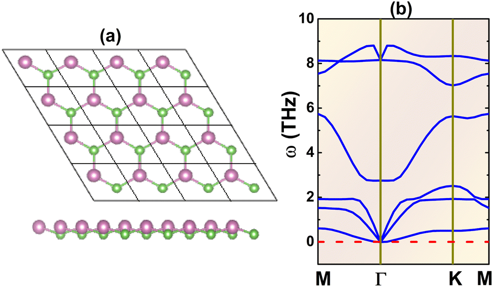
Fig. 1a shows a 4 × 4 × 1 supercell of the InAs monolayer. It can be noted that there are two inequivalent atoms (one In and one As atom) in a unit cell, located at different atomic planes and thus generating a buckled structure. Consequently, the structure belongs to the P3m1 space group (no. 156). After a full relaxation, the following structural parameters are obtained for the optimized unit cell: (1) lattice constant a = 4.38 Å; (2) buckling height ΔIn–As = 0.67 Å; (3) chemical bond length dIn–As = 2.61 Å; and (4) interatomic angles ∠InAsIn = ∠AsInAs = 113.68°. Once the structure is optimized, phonon dispersion curves are calculated. The spectra given in Fig. 1b provide evidence of dynamical stability considering the absence of imaginary phonon modes. Therefore, it can be concluded that the buckled honeycomb InAs monolayer is dynamically stable, and its ground-state properties will be further investigated.
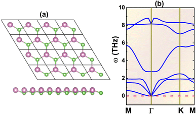 |
| | Fig. 1 (a) A 4 × 4 × 1 atomic model (In: purple balls; As: green balls) and (b) phonon dispersion curves of the InAs monolayer. | |
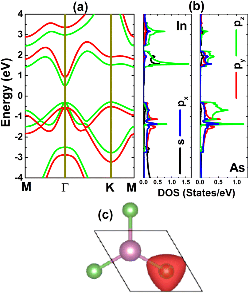
The electronic properties of the considered monolayer are investigated through its band structure, projected density of states (PDOS), and charge distribution. From Fig. 2a, one can see that the InAs monolayer is an indirect gap semiconductor, since the valence band and conduction band are clearly separated by a forbidden energy region, where the valence band maximum and conduction band minimum are found at the K and Γ point, respectively. An energy gap of 0.77 eV is obtained via the standard PBE functional, while a larger value of 1.41 eV is obtained from the HSE06-based calculations. These values are in good agreement with previous calculations by Liu et al.;24 however, a direct band gap was obtained in that work. It is worth mentioning that the difference between the valence band maximum at the Γ and K points is quite small (only 0.015 eV); therefore, the indirect or direct band gap character of the InAs monolayer is normally questionable. Moreover, this feature may suggest that the indirect–direct band gap transition can be easily induced by applying external factors. The PDOS spectra displayed in Fig. 2b indicate that the valence band is formed mainly from As-p orbitals, where the pz state dominates the upper part. Meanwhile, the In-pz state originates mainly in the lower part of the conduction band along with the In-s state. The PDOS profile may suggest significant electronic hybridization between the In-p and As-p orbitals, since they appear in the same energy range. However, it must be mentioned that there are ionic interactions between these atoms due to the difference in their electronegativity. The illustration of the charge distribution in Fig. 2c indicates charge transfer from the In to the As atom, considering significant charge accumulation at the As site, which is a result of the smaller electronegativity of In (1.78) in comparison with that of As (2.18).54 Additionally, this process is also confirmed by the Bader charge analysis, which asserts the transfer of a charge amount of 0.59e.
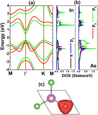 |
| | Fig. 2 (a) Electronic band structure (calculated with PBE – green curve and HSE06 – red curve), (b) projected density of states, and (c) charge distribution (iso-surface value: 0.05 e Å−3) of the InAs monolayer. | |
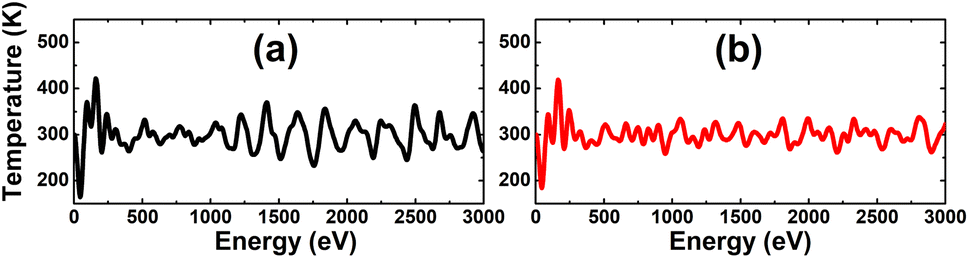
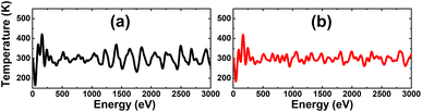
Before considering the doping, single In and As vacancies are investigated. Firstly, AIMD simulations are performed over the course of 3000 fs to examine the thermal stability of the defect-containing systems at room temperature. The results given in Fig. 3 indicate that the creation of vacancies leads to the formation of thermally stable systems, since no chemical bonds in the defect-contaning InAs monolayer are broken upon increasing temperature to 300 K.
 |
| | Fig. 3 AIMD simulations at 300 K for the InAs monolayer with (a) a single In vacancy and (b) a single As vacancy. | |
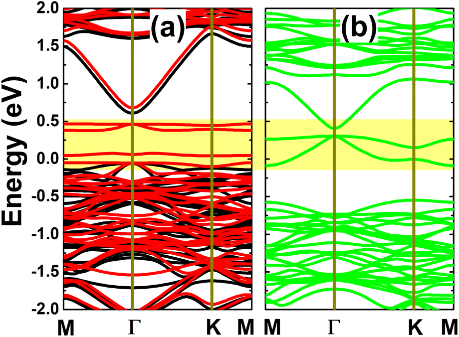
The spin-polarized calculation of band structures indicates a clear spin polarization in the case of the In vacancy, as displayed in Fig. 4a, mostly around the Fermi level with the appearance of new spin-down middle-gap flat energy branches. The band structure profile indicates a magnetic semiconducting nature induced by creating a single In vacancy in the InAs monolayer. Specifically, energy gaps of 0.66 and 0.09 eV are obtained in the spin-up and spin-down channels, respectively. The band structure profile suggests the defect-containing InAs monolayer with a single In vacancy is a prospective candidate for spintronic applications to generate a spin current by spin-filtering. In contrast, the band structure is totally spin-symmetric in the InAs monolayer with an As vacancy. In this case, the monolayer is metallized due to new middle-gap energy curves. Undoubtedly, the new middle-gap energy states in both cases originate from unsaturated chemical bonds, that is, the atoms closest to the defect site.
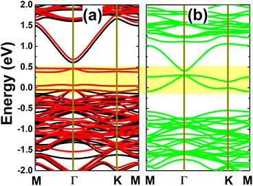 |
| | Fig. 4 Spin-resolved band structure (non spin-polarization: green curves; spin-up: black curves; spin-down: red curves; the Fermi level is set to 0 eV; new middle-gap states are indicated in the yellow-colored regions) of the InAs monolayer with (a) a single In vacancy and (b) a single As vacancy. | |
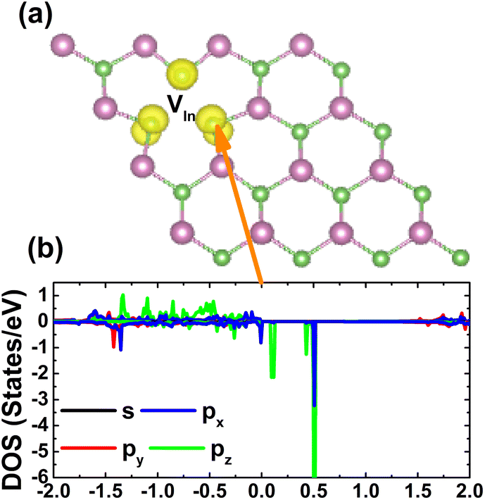
The spin asymmetry in the band structure may suggest significant magnetism in the InAs monolayer when creating a single In vacancy. Our calculations indicate a strong magnetization with a total magnetic moment of 2.98 μB. Fig. 5 shows the spin density and PDOS spectra for investigating the origin of the magnetism. From panel (a), one can see that the As atoms around the vacancy site are mainly responsible for the magnetization, while a smaller contribution comes from the other second As neighbor. The PDOS spectra of the main magnetizing atom given in panel (b) provide more insights into the role of each orbital. Note that the As-p orbital (with all px, py, and pz states) produces mainly magnetic properties, where the spin-down energy gap is formed by the separation between the occupied px,y state and the unoccupied pz state.
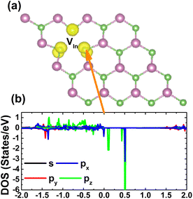 |
| | Fig. 5 (a) Spin density (iso-surface value: 0.008 e Å−3) in the InAs monolayer with a single In vacancy and (b) projected density of states of the As atom closest to the vacancy site. | |
3.2. Effects of n-doping
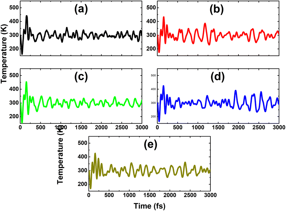
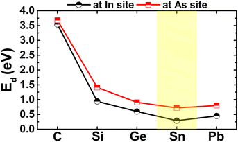
The calculated doping energies are listed in Table 1 and illustrated in Fig. 6. Note that C doping is energetically less favorable, with an Ed value of 3.54 eV, and Sn doping requires supplying the smallest energy of only 0.29 eV. These results are derived from the difference in atomic size of the In atom and IVA-group impurities. The atomic radii of In, C, Si, Ge, Sn, and Pb atoms are 155, 70, 110, 125, 145, and 180 pm,55 respectively, such that the differences in the atomic radii for In–C, In–Si, In–Ge, In–Sn, and In–Pb pairs are 85, 45, 30, 10, and 25 pm, respectively. In other words, the similar atomic size between the In and Sn atoms leads to the energetic favorability of the Sn doping process. Despite the differences in doping energy, all the n-doped systems are thermally stable at room temperature since the chemical bonds are well preserved after doping, without any structural destruction, as confirmed by the AIMD simulations in Fig. 7.
Table 1 Doping energy Ed (eV), spin-dependent band gap Eg (eV; M = metallic), charge transfer from dopant ΔQ (e; “−”: receiving charge; “+”: giving charge), and total magnetic moment Mt (μB) of the InAs monolayer doped with IVA-group atoms at In (n-doping) and As (p-doping) sites
|
|
|
E
d
|
E
upg
|
E
dng
|
ΔQ |
M
t
|
| n-doping |
C |
3.54 |
M |
M |
−0.88 |
0.00 |
| Si |
0.94 |
M |
M |
+0.80 |
0.00 |
| Ge |
0.60 |
0.29 |
0.60 |
+0.38 |
0.98 |
| Sn |
0.29 |
0.43 |
0.60 |
+0.55 |
1.00 |
| Pb |
0.45 |
0.64 |
0.37 |
+0.50 |
1.00 |
| p-doping |
C |
3.68 |
0.57 |
0.14 |
−0.92 |
1.00 |
| Si |
1.41 |
0.86 |
0.37 |
−0.28 |
1.00 |
| Ge |
0.91 |
0.87 |
0.24 |
−0.28 |
1.00 |
| Sn |
0.72 |
0.90 |
0.14 |
−0.09 |
1.00 |
| Pb |
0.80 |
0.86 |
M |
+0.05 |
1.00 |
 |
| | Fig. 6 Doping energy of IVA-group atoms in the InAs monolayer. | |
 |
| | Fig. 7 AIMD simulations at 300 K for the InAs monolayer with (a) CIn, (b) SiIn, (c) GeIn, (d) SnIn, and (e) PbIn doping (atomic structures after AIMD simulations are given in Fig. S1 of the ESI†). | |
Further spin-polarized calculations of the band structures indicate spin-symmetry in the C- and Si-doped systems, as observed in Fig. 8a and b. Note that the InAs monolayer is metallized by doping with C and Si. In contrast, spin polarization occurs in the Ge-, Sn-, and Pb-doped monolayers, as shown in Fig. 8c–e. In these cases, one flat energy branch emerges in the upper part of the spin-up valence band and the other appears in the lower part of the spin-down conduction band, giving rise to the formation of magnetic semiconductor 2D materials for spintronic applications. The spin-dependent energy gaps are given in Table 1. Note that the obtained values are considerably smaller than that of the pristine monolayer, which is a consequence of the new middle-gap energy states that are derived from the modified electronic interactions around the doping site. Bader charge analysis is performed to get insights into the interactions between the IVA-group impurities and host monolayer. Our calculations confirm that the C impurity acts as a charge acceptor, gaining a charge quantity of 0.88e, which is a result of its larger electronegativity than that of the As atom. Meanwhile, Si, Ge, Sn, and Pb atoms are less electronegative than the As atom; therefore, they lose charge when replacing the In atom in the InAs monolayer. Specifically, charge amounts of 0.80, 0.38, 0.55, and 0.50e, respectively, are transferred from these impurities to the host monolayer.
 |
| | Fig. 8 Spin-resolved band structure (non spin-polarization: green curves; spin-up: black curves; spin-down: red curves; the Fermi level is set to 0 eV; new middle-gap states are indicated in the yellow-colored regions) of the InAs monolayer with (a) CIn, (b) SiIn, (c) GeIn, (d) SnIn, and (e) PbIn doping. | |
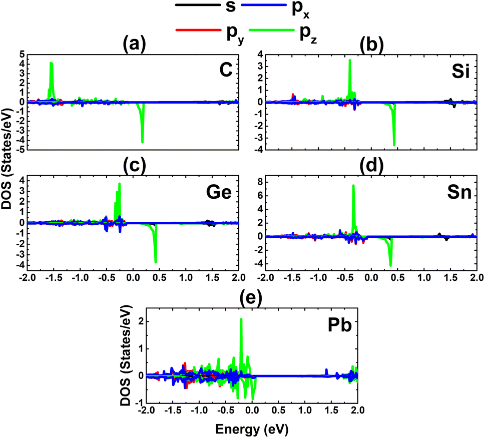
Now, the magnetic properties of the Ge-, Sn-, and Pb-doped systems are investigated, and are evidenced by the spin-asymmetric band structures. Firstly, the spin density is calculated to determine the magnetizing atoms. The illustrations in Fig. 9a–c imply that the difference in charge distribution between spin channels takes place mainly at the Ge, Sn, and Pb impurities and their first As neighbor atoms, indicating their key role in producing magnetism. Further investigation of the origin of the magnetism is based on the PDOS spectra, as displayed in Fig. 10, in which the C and Si dopants as well as their neighbors are analysed to explain the origin of the new middle-gap states. Note that in all cases, new middle-gap energy branches are derived from the pz state of the impurities and their neighbor As atoms. Consequently, this state regulates mainly the ground-state electronic and magnetic properties of the doped systems. The PDOS is spin-symmetric in the cases of C and Si doping, suggesting a spin-balanced charge distribution such that no magnetism is induced. Meanwhile, the pz state is only partially occupied to achieve magnetization of the monolayer by doping with Ge, Sn, and Pb. Moreover, the PDOS profiles and values may suggest that the electronic hybridization becomes stronger according to the increase in the atomic number of the IVA-group impurities. This feature attributes the absence of magnetism in the C- and Si-doped systems to the strong ionic interactions.
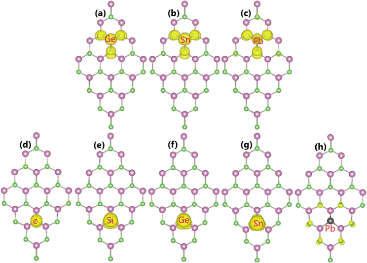 |
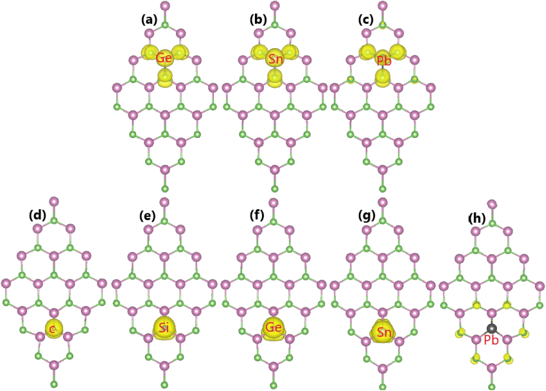
| | Fig. 9 Spin density (iso-surface value: 0.0015 e Å−3) in the InAs monolayer with (a) GeIn, (b) SnIn, (c) PbIn, (d) CAs, (e) SiAs, (f) GeAs, (g) SnAs, and (h) PbAs doping. | |
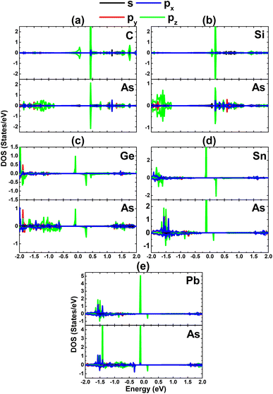 |
| | Fig. 10 Projected density of states of the dopant and its neighbor As atom for the InAs monolayer with (a) CIn, (b) SiIn, (c) GeIn, (d) SnIn, and (e) PbIn doping. | |
3.3. Effects of p-doping
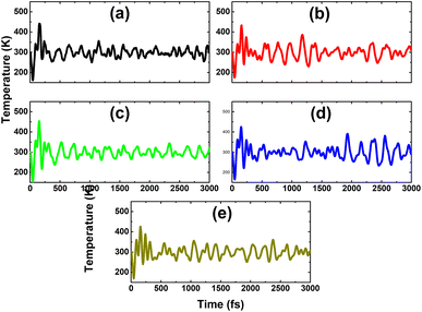
From Table 1 and Fig. 6, one can see that n-doping may require a smaller additional energy than p-doping, where the variation in the doping energy is quite similar, decreasing from C though to Sn impurities, and then this parameter increases for the Pb dopant. Therefore, Sn doping is also energetically the most favorable in the cases of p-doping. It is worth mentioning that the As atom acts as a charge acceptor, therefore the doping energy is not only determined by the difference in atomic size, but also by the interactions between the IVA-impurities and their environment. Herein, the Sn atom may have higher affinity for the In atom due to their similar atomic sizes and valence electronic configurations. Further AIMD simulations for the p-doped systems indicate their good thermal stability at room temperature, since the constituent atoms vibrate around their equilibrium sites upon increasing the temperature to 300 K, without breaking the chemical bonds, as displayed in Fig. 11.
 |
| | Fig. 11 AIMD simulations at 300 K for the InAs monolayer with (a) CAs, (b) SiAs, (c) GeAs, (d) SnAs, and (e) PbAs doping (atomic structures after AIMD simulations are given in Fig. S2 of the ESI†). | |
Fig. 12 shows the spin-polarized band structures of the p-doped InAs monolayers. It can be noted that there is a clear spin polarization in all cases, suggesting doping-induced magnetization, which will be analyzed below. The semiconducting character is maintained in both spin configurations of the C-, Si-, Ge-, and Sn-doped systems, generating a magnetic semiconductor, where the flat middle-gap energy branch may significantly reduce the spin-down energy gap. Meanwhile, this middle-gap energy curve is submerged into the upper part of the valence band, giving the metallic spin-down state of the Pb-doped monolayer, such that half-metallicity, with 100% spin polarization around the Fermi level, emerges to functionalize the InAs monolayer for spintronic applications. All the band gaps of the semiconductor spin channels are listed in Table 1. The Bader charge analysis indicates that C, Si, Ge, and Sn impurities act as charge acceptors in the InAs monolayer, gaining charge quantities of 0.92, 0.28, 0.28, and 0.09e, respectively. Note that this parameter decreases according to an increase in the atomic number of the IVA-group impurity. These results suggest a reduction of the ionic character in the chemical bonds between the impurities and their neighbor In atoms. In contrast, the Pb dopant loses charge, transferring an amount of 0.05e to the host monolayer.
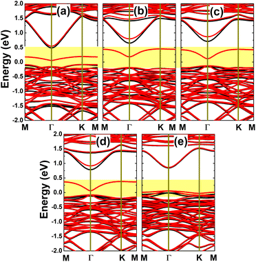 |
| | Fig. 12 Spin-resolved band structure (spin-up: black curves; spin-down: red curves; the Fermi level is set to 0 eV; new middle-gap states are indicated in the yellow-colored regions) of the InAs monolayer with (a) CAs, (b) SiAs, (c) GeAs, (d) SnAs, and (e) PbAs doping. | |
Our calculations demonstrate that the InAs monolayer is magnetized by p-doping using IVA-group impurities, which is reflected in the spin-polarized band structures, as analyzed above. Moreover, a total magnetic moment of 1.00 μB is obtained by doping with C, Si, Ge, and Sn at the As site. In these cases, the dopant atoms are the main contributors to the magnetism, as confirmed by the spin density illustrated in Fig. 9d–g. Meanwhile, a weaker magnetization is induced by Pb doping, with a smaller total magnetic moment of 0.69 μB, where the magnetic properties are produced mainly by the As atoms closest to the doping site (See Fig. 9h). Further analysis of the PDOS spectra of the magnetic atoms in Fig. 13 indicates the key role of the pz state of the IVA-group impurities in magnetizing the InAs monolayer. From the figure, it can be noted that there is a new flat spin-up state entirely submerged into the valence band, such that it is not clearly identified in the band structures. Similarly, the As-pz state is the main origin of the magnetism of the Pb-doped monolayer, suggesting that As atoms mainly receive the charge transferred from the Pb dopant.
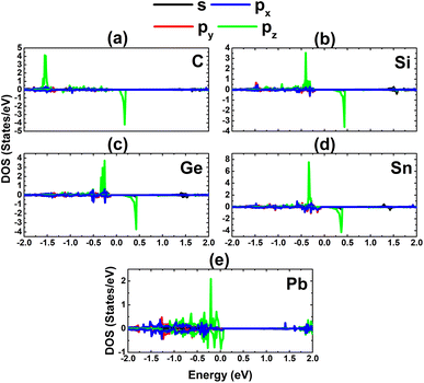 |
| | Fig. 13 Projected density of states of the magnetic atoms in the InAs monolayer with (a) CAs, (b) SiAs, (c) GeAs, (d) SnAs, and (e) PbAs doping. | |
3.4. Highly doped systems
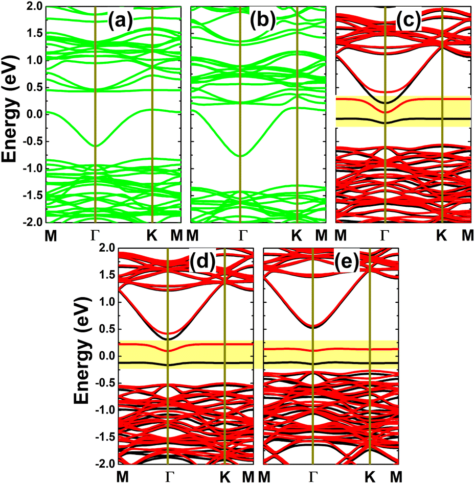
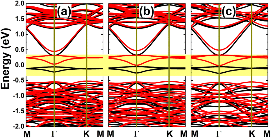
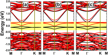
It has been asserted that n-doping by replacing an In atom with an Sn atom is energetically most favorable. Therefore, a further investigation on the doping level is realized for this case, by substituting two, three, or four In atoms in a 4 × 4 × 1 supercell to get doping levels of 12.5%, 18.75%, and 25%, respectively. Fig. 14 shows the spin-polarized band structures of the highly doped systems. It can be noted that there are new middle-gap energy curves, but spreading in a wider energy range in comparison with the case of 6.25% doping. The spin polarization is observed mainly in the vicinity of the Fermi level. A magnetic semiconducting nature is achieved with the 12.5% dopant composition, with spin-up and spin-down energy gaps of 0.37 and 0.55 eV, respectively. Meanwhile, half-metallicity is induced by higher doping levels of 18.75% and 25%, with spin-down band gaps of 0.38 and 0.37 eV, respectively.
 |
| | Fig. 14 Spin-resolved band structure (spin-up: black curves; spin-down: red curves; the Fermi level is set to 0 eV; new middle-gap states are indicated in the yellow-colored regions) of the InAs monolayer doped with (a) 12.5%, (b) 18.75%, and (c) 25% Sn. | |
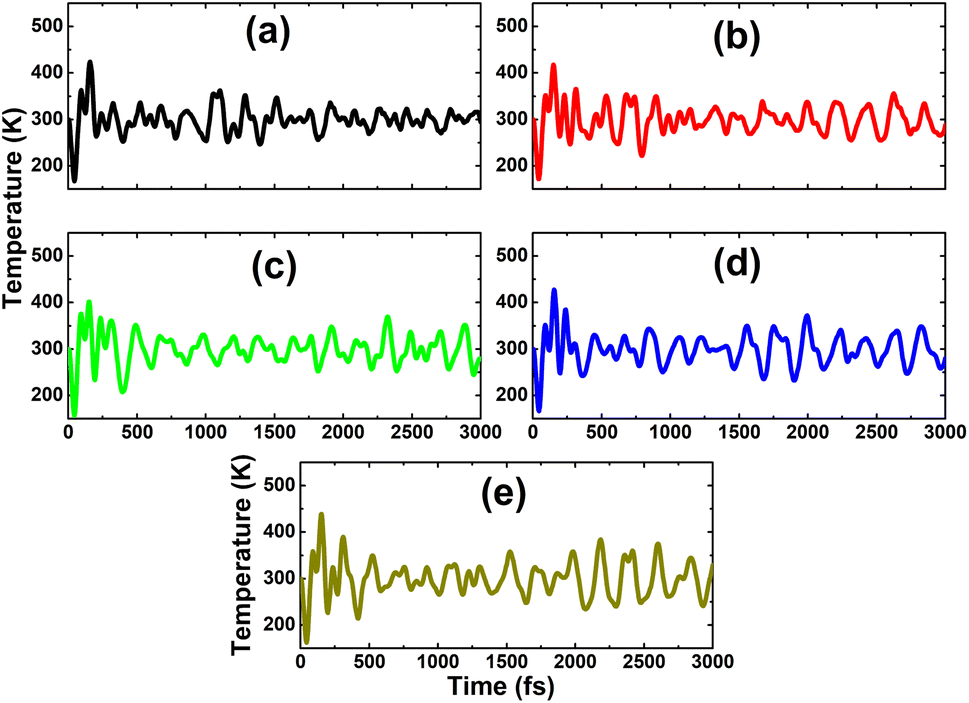
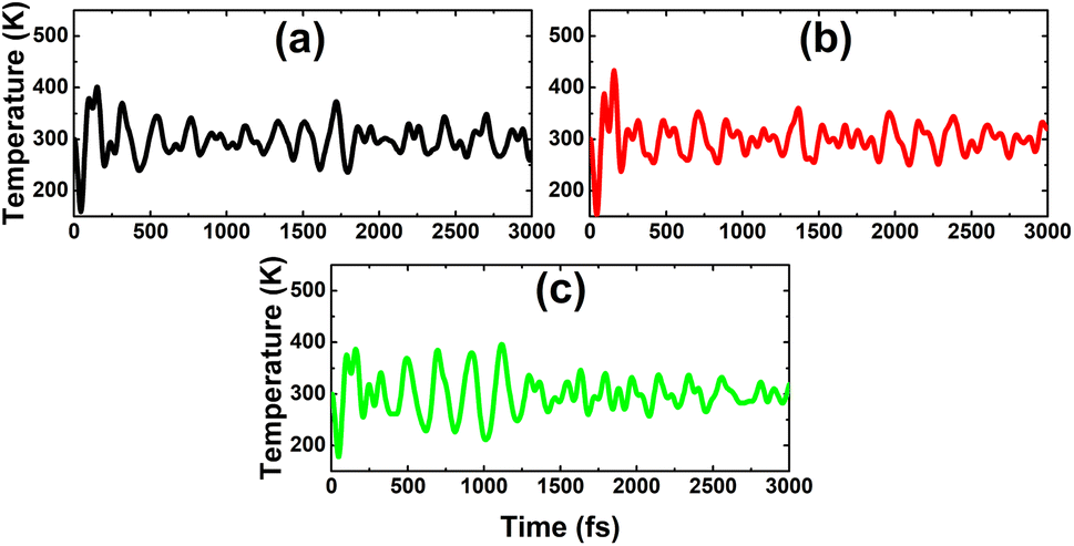
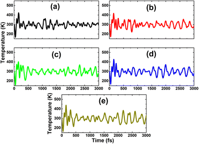
As expected, a higher doping level leads to a stronger magnetization of the monolayer, such that total magnetic moments of 1.98, 2.93, and 3.92 μB are obtained with 12.5%, 18.75%, and 25% Sn impurities in the InAs monolayer, respectively. The illustration of the spin density displayed in Fig. 15 indicates that the Sn impurities and their neighbor As atoms play a key role as magnetic atoms. It is undoubted that the magnetism originates mainly from their pz states, similar to the case of low doping. Finally, the thermal stability of the highly doped systems at room temperature is also examined via AIMD simulations. Simulations performed at room temperature suggest stable chemical bonds under the effects of temperature when it is increased up to 300 K, as confirmed by the AIMD results in Fig. 16, indicating that the doped systems are thermally stable.
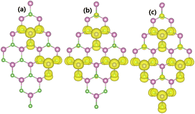 |
| | Fig. 15 Spin density (iso-surface value: 0.0015 e Å−3) in the InAs monolayer doped with (a) 12.5%, (b) 18.75%, and (c) 25% Sn. | |
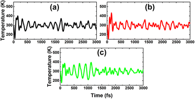 |
| | Fig. 16 AIMD simulations at 300 K for the InAs monolayer doped with (a) 12.5%, (b) 18.75%, and (c) 25% Sn. | |
4. Conclusions
In conclusion, the effects of doping with IVA-group atoms on the electronic and magnetic properties of a low-buckled honeycomb InAs monolayer have been systematically investigated using DFT-based first-principles calculations. The pristine monolayer exhibits good dynamical stability and a semiconducting nature with a mix of covalent and ionic characters. A single In vacancy significantly magnetizes the monolayer, giving rise to the appearance of a magnetic semiconductor behavior, where the magnetic properties are produced mainly by the p orbitals of the As atoms around the defect site. Meanwhile, it is metallized by a single As vacancy. n-Doping in the In sublattice may be energetically more favorable than p-doping at the As site, where Sn doping requires the smallest supply of energy. The metallization and magnetic semiconducting nature are induced by C–Si and Ge–Sn–Pb n-doping at the In site. Herein, magnetism originates mainly from the unbalanced charge distribution between the spin channels of the pz state of the dopants and their neighbor As atoms. Similarly, new middle-gap states regulate the ground state of the p-doped systems, where magnetic semiconducting and half-metallic behaviors are obtained by doping with C–Si–Ge–Sn and Pb, respectively. In all cases, the pz state of the impurities and As atoms, respectively, produces mainly magnetic properties. It has been also found that the monolayer is more strongly magnetized upon increasing the doping level, where the transition from magnetic semiconducting to half-metallic behavior may occur in the highly doped systems. AIMD simulations confirm that the structural configurations are well-preserved upon increasing temperature, indicating good thermal stability of all the considered systems at room temperature. This work may pave a solid path to making prospective 2D InAs-based spintronic materials, and suggests doping with IVA-group atoms as an efficient method to functionalize III–V group monolayers.
Data availability
The data that support the findings of this study are available from the corresponding author upon request.
Conflicts of interest
The authors declare that they have no known competing financial interests or personal relationships that could have appeared to influence the work reported in this paper.
Acknowledgements
Calculations were performed at the DGCTIC-UNAM Supercomputing Center (projects LANCAD-UNAM-DGTIC-368). D. M. Hoat expresses his gratitude for all the valuable support from Duy Tan University, which is going to celebrate its 30th anniversary of establishment (Nov. 11, 1994–Nov. 11, 2024) towards “Integral, Sustainable and Stable Development”.
References
- K. S. Novoselov, A. K. Geim, S. V. Morozov, D.-e. Jiang, Y. Zhang, S. V. Dubonos, I. V. Grigorieva and A. A. Firsov, Electric field effect in atomically thin carbon films, Science, 2004, 306(5696), 666–669 CrossRef CAS PubMed.
- S. Kumar, N. McEvoy, H.-Y. Kim, K. Lee, N. Peltekis, E. Rezvani, H. Nolan, A. Weidlich, R. Daly and G. S. Duesberg, Cvd growth and processing of graphene for electronic applications, Phys. Status Solidi B, 2011, 248(11), 2604–2608 CrossRef CAS.
- B. Sensale-Rodriguez, Graphene-based optoelectronics, J. Lightwave Technol., 2015, 33(5), 1100–1108 CAS.
- F. Bonaccorso, Z. Sun, T. Hasan and A. Ferrari, Graphene photonics and optoelectronics, Nat. Photonics, 2010, 4(9), 611–622 CrossRef CAS.
- M. Romagnoli, V. Sorianello, M. Midrio, F. H. Koppens, C. Huyghebaert, D. Neumaier, P. Galli, W. Templ, A. D'Errico and A. C. Ferrari, Graphene-based integrated photonics for next-generation datacom and telecom, Nat. Rev. Mater., 2018, 3(10), 392–414 CrossRef CAS.
- A. G. Olabi, M. A. Abdelkareem, T. Wilberforce and E. T. Sayed, Application of graphene in energy storage device–a review, Renewable Sustainable Energy Rev., 2021, 135, 110026 CrossRef CAS.
- J. Zhu, D. Yang, Z. Yin, Q. Yan and H. Zhang, Graphene and graphene-based materials for energy storage applications, Small, 2014, 10(17), 3480–3498 CrossRef CAS PubMed.
- S. S. Varghese, S. Lonkar, K. Singh, S. Swaminathan and A. Abdala, Recent advances in graphene based gas sensors, Sens. Actuators, B, 2015, 218, 160–183 CrossRef CAS.
- S. Basu and P. Bhattacharyya, Recent developments on graphene and graphene oxide based solid state gas sensors, Sens. Actuators, B, 2012, 173, 1–21 CrossRef CAS.
- C. Huang, C. Li and G. Shi, Graphene based catalysts, Energy Environ. Sci., 2012, 5(10), 8848–8868 RSC.
- B. F. Machado and P. Serp, Graphene-based materials for catalysis, Catal. Sci. Technol., 2012, 2(1), 54–75 RSC.
- W. Han, R. K. Kawakami, M. Gmitra and J. Fabian, Graphene spintronics, Nat. Nanotechnol., 2014, 9(10), 794–807 CrossRef CAS PubMed.
- O. V. Yazyev, Emergence of magnetism in graphene materials and nanostructures, Rep. Prog. Phys., 2010, 73(5), 056501 CrossRef.
- A. Gupta, T. Sakthivel and S. Seal, Recent development in 2D materials beyond graphene, Prog. Mater. Sci., 2015, 73, 44–126 CrossRef CAS.
- S. Z. Butler, S. M. Hollen, L. Cao, Y. Cui, J. A. Gupta, H. R. Gutiérrez, T. F. Heinz, S. S. Hong, J. Huang and A. F. Ismach,
et al., Progress, challenges, and opportunities in two-dimensional materials beyond graphene, ACS Nano, 2013, 7(4), 2898–2926 CrossRef CAS PubMed.
- X. Li, X. Hao, M. Zhao, Y. Wu, J. Yang, Y. Tian and G. Qian, Exfoliation of hexagonal boron nitride by molten hydroxides, Adv. Mater., 2013, 25(15), 2200–2204 CrossRef CAS PubMed.
- J. H. Warner, M. H. Rummeli, A. Bachmatiuk and B. Buchner, Atomic resolution imaging and topography of boron nitride sheets produced by chemical exfoliation, ACS Nano, 2010, 4(3), 1299–1304 CrossRef CAS PubMed.
- D. Hoat, M. Naseri, R. Ponce-Pérez, N. N. Hieu, T. V. Vu, J. Rivas-Silva and G. H. Cocoletzi, Reducing the electronic band gap of BN monolayer by coexistence of P(As)-doping and external electric field, Superlattices Microstruct., 2020, 137, 106357 CrossRef CAS.
- H. Yang, L. Wang, F. Gao, M. Dai, Y. Hu, H. Chen, J. Zhang, Y. Qiu, Y. Zhou and P. Hu,
et al., Shape evolution of two dimensional hexagonal boron nitride single domains on Cu/Ni alloy and its applications in ultraviolet detection, Nanotechnology, 2019, 30(24), 245706 CrossRef CAS PubMed.
- H. Liu, J. Meng, X. Zhang, Y. Chen, Z. Yin, D. Wang, Y. Wang, J. You, M. Gao and P. Jin, High-performance deep ultraviolet photodetectors based on few-layer hexagonal boron nitride, Nanoscale, 2018, 10(12), 5559–5565 RSC.
- J. Ben, X. Liu, C. Wang, Y. Zhang, Z. Shi, Y. Jia, S. Zhang, H. Zhang, W. Yu and D. Li,
et al., 2D III-Nitride materials: Properties, growth, and applications, Adv. Mater., 2021, 33(27), 2006761 CrossRef CAS.
- S. Sarikurt, Y. Z. Abdullahi, E. Durgun and F. Ersan, Negative thermal expansion of group III-Nitride monolayers, J. Phys. D: Appl. Phys., 2022, 55(31), 315303 CrossRef.
- T. Suzuki, Theoretical discovery of stable structures of group III-V monolayers: The materials for semiconductor devices, Appl. Phys. Lett., 2015, 107(21), 213105 CrossRef.
- X.-F. Liu, Z.-J. Luo, X. Zhou, J.-M. Wei, Y. Wang, X. Guo, B. Lv and Z. Ding, Structural, mechanical, and electronic properties of 25 kinds of III–V binary monolayers: A computational study with first-principles calculation, Chin. Phys. B, 2019, 28(8), 086105 CrossRef CAS.
- A. Hirohata, K. Yamada, Y. Nakatani, I.-L. Prejbeanu, B. Diény, P. Pirro and B. Hillebrands, Review on spintronics: Principles and device applications, J. Magn. Magn. Mater., 2020, 509, 166711 CrossRef CAS.
- I. Žutić, J. Fabian and S. D. Sarma, Spintronics: Fundamentals and applications, Rev. Mod. Phys., 2004, 76(2), 323 CrossRef.
- X. Li and J. Yang, First-principles design of spintronics materials, Natl. Sci. Rev., 2016, 3(3), 365–381 CrossRef CAS.
- C. Felser, G. H. Fecher and B. Balke, Spintronics: a challenge for materials science and solid-state chemistry, Angew. Chem., Int. Ed., 2007, 46(5), 668–699 CrossRef CAS PubMed.
- E. C. Ahn, 2D materials for spintronic devices, npj 2D Mater. Appl., 2020, 4(1), 17 CrossRef CAS.
- X. Li and X. Wu, Two-dimensional monolayer designs for spintronics applications, Wiley Interdiscip. Rev.: Comput. Mol. Sci., 2016, 6(4), 441–455 CAS.
- S. K. Gupta,
et al., Effect of Si doping on the electronic properties of BN monolayer, Nanoscale, 2014, 6(10), 5526–5531 RSC.
- I. Choudhuri and B. Pathak, Ferromagnetism and half-metallicity in a high-band-gap hexagonal boron nitride system, ChemPhysChem, 2018, 19(1), 153–161 CrossRef CAS.
- Y. Kadioglu, F. Ersan, D. Kecik, O. Ü. Aktürk, E. Aktürk and S. Ciraci, Chemical and substitutional doping, and anti-site and vacancy formation in monolayer AlN and GaN, Phys. Chem. Chem. Phys., 2018, 20(23), 16077–16091 RSC.
- B. Peng, D. Zhang, H. Zhang, H. Shao, G. Ni, Y. Zhu and H. Zhu, The conflicting role of buckled structure in phonon transport of 2D group-IV and group-V materials, Nanoscale, 2017, 9(22), 7397–7407 RSC.
- A. Molle, J. Goldberger, M. Houssa, Y. Xu, S.-C. Zhang and D. Akinwande, Buckled two-dimensional Xene sheets, Nat. Mater., 2017, 16(2), 163–169 CrossRef CAS PubMed.
- W. Zhang, H. Enriquez, Y. Tong, A. Bendounan, A. Kara, A. P. Seitsonen, A. J. Mayne, G. Dujardin and H. Oughaddou, Epitaxial synthesis of blue phosphorene, Small, 2018, 14(51), 1804066 CrossRef.
- H. Zhang, M. Holbrook, F. Cheng, H. Nam, M. Liu, C.-R. Pan, D. West, S. Zhang, M.-Y. Chou and C.-K. Shih, Epitaxial growth of two-dimensional insulator monolayer honeycomb BeO, ACS Nano, 2021, 15(2), 2497–2505 CrossRef CAS PubMed.
- C. Polley, H. Fedderwitz, T. Balasubramanian, A. Zakharov, R. Yakimova, O. Bäcke, J. Ekman, S. Dash, S. Kubatkin and S. Lara-Avila, Bottom-up growth of monolayer honeycomb SiC, Phys. Rev. Lett., 2023, 130(7), 076203 CrossRef CAS PubMed.
- H. Şahin, S. Cahangirov, M. Topsakal, E. Bekaroglu, E. Akturk, R. T. Senger and S. Ciraci, Monolayer honeycomb structures of group-IV elements and III-V binary compounds: First-principles calculations, Phys. Rev. B: Condens. Matter Mater. Phys., 2009, 80(15), 155453 CrossRef.
- W. Yu, J. Li, Y. Wu, J. Lu and Y. Zhang, Systematic investigation of the mechanical, electronic, and interfacial properties of high mobility monolayer InAs from first-principles calculations, Phys. Chem. Chem. Phys., 2023, 25(15), 10769–10777 RSC.
- W. Kohn and L. J. Sham, Self-consistent equations including exchange and correlation effects, Phys. Rev., 1965, 140(4A), A1133 CrossRef.
- G. Kresse and J. Furthmüller, Efficiency of ab initio total energy calculations for metals and semiconductors using a plane-wave basis set, Comput. Mater. Sci., 1996, 6(1), 15–50 CrossRef CAS.
- G. Kresse and J. Furthmüller, Efficient iterative schemes for ab initio total-energy calculations using a plane-wave basis set, Phys. Rev. B: Condens. Matter Mater. Phys., 1996, 54(16), 11169 CrossRef CAS PubMed.
- J. P. Perdew, K. Burke and M. Ernzerhof, Generalized gradient approximation made simple, Phys. Rev. Lett., 1996, 77(18), 3865 CrossRef CAS PubMed.
- A. V. Krukau, O. A. Vydrov, A. F. Izmaylov and G. E. Scuseria, Influence of the exchange screening parameter on the performance of screened hybrid functionals, J. Chem. Phys., 2006, 125(22), 224106 CrossRef PubMed.
- H. J. Monkhorst and J. D. Pack, Special points for Brillouin-zone integrations, Phys. Rev. B: Solid State, 1976, 13(12), 5188 CrossRef.
- M. Rafique, Y. Shuai and N. Hussain, First-principles study on silicon atom doped monolayer graphene, Phys. E, 2018, 95, 94–101 CrossRef CAS.
- A. Togo, First-principles phonon calculations with phonopy and phono3py, J. Phys. Soc. Jpn., 2023, 92(1), 012001 CrossRef.
- B. Luo, Y. Yao, E. Tian, H. Song, X. Wang, G. Li, K. Xi, B. Li, H. Song and L. Li, Graphene-like monolayer monoxides and monochlorides, Proc. Natl. Acad. Sci. U. S. A., 2019, 116(35), 17213–17218 CrossRef CAS PubMed.
- A. Bafekry, M. Naseri, M. Faraji, M. Fadlallah, D. Hoat, H. Jappor, M. Ghergherehchi, D. Gogova and H. Afarideh, Theoretical prediction of two-dimensional BC2X (X= N, P, As) monolayers: ab initio investigations, Sci. Rep., 2022, 12(1), 22269 CrossRef CAS PubMed.
- W. Tang, E. Sanville and G. Henkelman, A grid-based Bader analysis algorithm without lattice bias, J. Phys.: Condens. Matter, 2009, 21(8), 084204 CrossRef CAS PubMed.
- M. Yu and D. R. Trinkle, Accurate and efficient algorithm for Bader charge integration, J. Chem. Phys., 2011, 134(6), 064111 CrossRef PubMed.
- Y. Mogulkoc, R. Caglayan and Y. Ciftci, Band alignment in monolayer boron phosphide with Janus MoSSe heterobilayers under strain and electric field, Phys. Rev. Appl., 2021, 16(2), 024001 CrossRef CAS.
- L. C. Allen, Electronegativity is the average one-electron energy of the valence-shell electrons in ground-state free atoms, J. Am. Chem. Soc., 1989, 111(25), 9003–9014 CrossRef CAS.
- J. C. Slater, Atomic radii in crystals, J. Chem. Phys., 1964, 41(10), 3199–3204 CrossRef CAS.
|
| This journal is © The Royal Society of Chemistry 2024 |
Click here to see how this site uses Cookies. View our privacy policy here. 
 Open Access Article
 This Open Access Article is licensed under a Creative Commons Attribution-Non Commercial 3.0 Unported Licence
 *ab and
J.
Guerrero-Sanchez
c
*ab and
J.
Guerrero-Sanchez
c