DOI:
10.1039/D3NA00343D
(Paper)
Nanoscale Adv., 2024,
6, 1091-1105
Interfacial negative magnetization in Ni encapsulated layer-tunable nested MoS2 nanostructure with robust memory applications†
Received
19th May 2023
, Accepted 3rd November 2023
First published on 10th November 2023
Abstract
Combining interfacial interactions and layer-number tunability, the evolution of magnetism in low-dimensional diamagnetic systems like MoS2 is indeed an interesting area of research. To explore this, Ni nanophases with an average size of 12 nm were encapsulated in MoS2 and the magnetization dynamics were studied over the temperature range of 2–300 K. Surprisingly, the newly formed hybrid nanostructure was found to have a negative magnetization state with giant exchange bias that showed a reversible temperature-induced increase in both spin magnetic moment and coercivity. Density functional theory calculations proved an interfacial charge transfer interaction with a spin-polarized density of states. The magnetization state, along with giant exchange correlation among the magnetic clusters, suggested the possibility of robust thermomagnetic memory. The dc magnetization and relaxation, investigated with different measurement protocols, unveiled robust thermoremanent magnetization as a memory effect. The time-dependent magnetization study indicated that contributions from the negative magnetization state along with charge transfer induced spin states are responsible for the memory effect, which can be controlled by both temperature and external field.
1. Introduction
During the past few years, intensive studies have been carried out on two-dimensional (2D) transition-metal (TM)-based nanostructures grown on graphene and MoS2 surfaces.1–3 Although many intriguing results on TM-based 2D surfaces have been demonstrated, the appearance of a negative magnetization state while inducing magnetism in diamagnetic MoS2 has not yet been discussed.
Since the proposal of the Néel temperature, certain ferrimagnets (spinel oxides) have exhibited spontaneous negative magnetization states that change with temperature and magnetic field.4–8 The observation of magnetization reversal has attracted much attention due to its enormous future applications in information storage and thermomagnetic switches.9–12 The negative state is due to the different temperature dependences of the sublattice magnetization originating from the structural contributions. Recently, some mixed ferrites, orthovanadates and rare-earth chromates also showed negative magnetization states due to such a reason.6–8 In these results, different magnetic elements were mixed at various sub-lattice sites with antiparallel arrangements. Consequently, inequivalent sites were already present in these cases. These observations have, however, been limited to generic ferrite or ferrimagnetic structures to date.
In the present study, we break the symmetry requirement for negative magnetization states in 2D systems by introducing a novel caged structure of MoS2 encapsulating Ni nanophases. The interface coupling has been modulated via the number of layers of MoS2. So far, Ni–MoS2 hybrid structures have mostly been experimentally studied for hydrogen evolution and catalytic activity enhancement.13,14 However, in the context of electronic and magnetic studies of the Ni–MoS2 system, the experimental literature is limited.15,16 This is mainly due to the instability of the metallic Ni nanophase on 2D surfaces. In the present work, we have successfully stabilized the Ni nanostructure by encapsulating it within nested MoS2 cages. This type of caged MoS2 nanostructure under precise high temperature treatment is thermodynamically more stable than the isolated lamellar structure.17,18 The large activation energy needed for bending the 2D structure is achieved in this case via a simple high temperature synthesis route.
Our first-principles density functional theory (DFT) calculations prove that interfacial charge transfer interactions can result in a gapless density of states (DOS) with 15% spin polarization. Because of the proximity-induced charge transfer between Ni and MoS2 at the interface, the electronic and magnetic characteristics are greatly modified from their pristine phases.19,20 It is found that temperature and magnetic field have competitive roles in controlling the effects at the interface. By tuning the number of layers in MoS2, we have achieved an enhancement in coercivity (141%) and magnetization (27.6 emu g−1) with temperature, while these parameters usually decrease with temperature due to thermal fluctuation.20 We observed an unusual temperature-induced increment in magnetic anisotropy, which usually decreases with temperature. Generation of antiferromagnetic coupling due to oppositely aligned spin components at the interface is the main reason behind these phenomena. The soft ferromagnetic contribution from the Ni phase and strong antiferromagnetic coupling at the interface between MoS2 and Ni result in large exchange splitting in the heterostructure (−2259 Oe bias field).
The giant enhancement in coercivity along with the exchange bias suggests the possibility of observing a hysteretic memory effect in 2D MoS2 hybrid systems.20 In contrast to usual magnetic media, temperature is used as a parameter to read/write the magnetization states. This creates a new class of phenomena that are termed thermomagnetic 2D memory. To understand the spin dynamics, we have performed in-depth dc relaxations using different protocols. Surprisingly, the system is able to memorize its magnetization state at elevated temperatures of 100–300 K. Even after a forced large jump in the magnetization history (294% under zero-field cooling, 175% under field-cooling) it can recall its initial level quickly. The wait-time dependence and ageing effect (several hours) have also been investigated to evaluate the robustness of the memory effect for practical applications. A stretched exponential function is used to evaluate the relaxation parameters (β and τ). Correlation among the parameters is explained on the basis of thermoremanent magnetization, which reveals the applicability of Ni encapsulated in MoS2 for 2D-based memory devices.
2. Experiments
2.1. Synthesis of MoS2 wrapping nested Ni nanostructures
To synthesize molybdenum disulphide sheets, 5 mM (310 mg) hexaammonium heptamolybdate tetrahydrate and 70 mM (267 mg) thiourea were dissolved in 50 ml of deionized water under continuous stirring to form a homogeneous solution. The number of layers was restricted by using cetyltrimethyl ammonium bromide (CTAB) as a cationic surfactant. For the first sample, 9.11 mg (0.05 mM) of CTAB was used. The final solution was transferred to a 50 ml Teflon-lined stainless steel autoclave for 24 h at 200 °C. The resultant product was washed several times in ethanol and water to remove all unreacted elements, then dried at 60 °C under vacuum. In the second step, the as-synthesized MoS2 powder was dispersed in 100 ml of DMF under ultrasonic vibration for 1 h. The well-dispersed MoS2 solution was placed in a round-bottom flask and kept at a temperature of 80 °C. For the Ni precursor, we used 5 mM Ni(AC)2 [AC: acetate] and added it to the MoS2 solution slowly under continuous stirring at 80 °C. After completion of the reaction, the powder was separated from the solution using a centrifuge at 10![[thin space (1/6-em)]](https://www.rsc.org/images/entities/char_2009.gif) 000 rpm and dispersed completely into double-distilled water. This solution mixture was again placed in a Teflon-lined steel autoclave for hydrothermal treatment at 180 °C for 10 h. During this hydrothermal process, a Ni(OH)2 phase was grown on the MoS2 surface. The product was washed with water and ethanol repeatedly. The final product was dried in a vacuum oven at 60 °C to get a MoS2/Ni(OH)2 composite. For the reduction of Ni(OH)2 to a metallic Ni phase, the composite powder was transferred into a 3-zone chemical vapor deposition (CVD) furnace where ultra-high purity (UHP) H2 gas was used at 600 °C for 1 h. During the reduction process, Ni(OH)2 was reduced to metallic Ni nanoparticles, which were wrapped by the MoS2 layers at high temperature. To control the number of layers of MoS2, we synthesized another two batches of samples, tuning the amount of surfactant CTAB to 1 mM and 3 mM. With increasing amount of surfactant, the thickness of the MoS2 layers was decreased. The role of the surfactant is to restrict the vertical growth of the MoS2 layers. Temperature also has a role in tuning the number of layers in the nested structure. For the higher concentrations of CTAB, we changed the reduction temperature in the CVD furnace to 550 and 450 °C. During the high-temperature heat treatment under a H2 atmosphere, metallic Ni phases were grown and simultaneously wrapped by MoS2 for the formation of an onion-like structure. The sample names were designated as M1, M2 and M3. M1 has the highest average number of MoS2 layers, while M2 and M3 have consecutively lower numbers of layers. It is well-known that with a high-temperature sintering process, such sheet-like lamellae are wrapped to form ‘inorganic-fullerene’-like caged structures.17,18 Large energies are needed to overcome the activation barrier associated with bending, which is supplied in this case by the heat-treatment process in the CVD furnace (450–600 °C).
000 rpm and dispersed completely into double-distilled water. This solution mixture was again placed in a Teflon-lined steel autoclave for hydrothermal treatment at 180 °C for 10 h. During this hydrothermal process, a Ni(OH)2 phase was grown on the MoS2 surface. The product was washed with water and ethanol repeatedly. The final product was dried in a vacuum oven at 60 °C to get a MoS2/Ni(OH)2 composite. For the reduction of Ni(OH)2 to a metallic Ni phase, the composite powder was transferred into a 3-zone chemical vapor deposition (CVD) furnace where ultra-high purity (UHP) H2 gas was used at 600 °C for 1 h. During the reduction process, Ni(OH)2 was reduced to metallic Ni nanoparticles, which were wrapped by the MoS2 layers at high temperature. To control the number of layers of MoS2, we synthesized another two batches of samples, tuning the amount of surfactant CTAB to 1 mM and 3 mM. With increasing amount of surfactant, the thickness of the MoS2 layers was decreased. The role of the surfactant is to restrict the vertical growth of the MoS2 layers. Temperature also has a role in tuning the number of layers in the nested structure. For the higher concentrations of CTAB, we changed the reduction temperature in the CVD furnace to 550 and 450 °C. During the high-temperature heat treatment under a H2 atmosphere, metallic Ni phases were grown and simultaneously wrapped by MoS2 for the formation of an onion-like structure. The sample names were designated as M1, M2 and M3. M1 has the highest average number of MoS2 layers, while M2 and M3 have consecutively lower numbers of layers. It is well-known that with a high-temperature sintering process, such sheet-like lamellae are wrapped to form ‘inorganic-fullerene’-like caged structures.17,18 Large energies are needed to overcome the activation barrier associated with bending, which is supplied in this case by the heat-treatment process in the CVD furnace (450–600 °C).
2.2. Powder X-ray diffraction analysis for phase identification
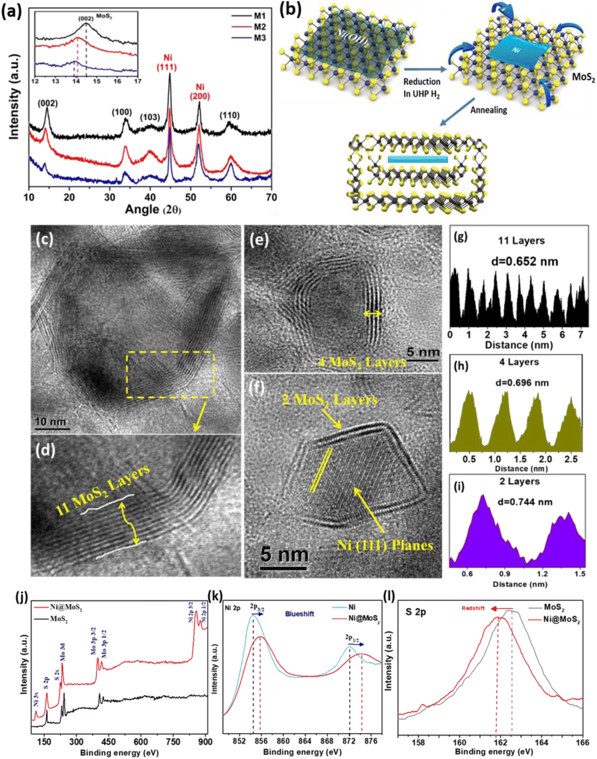
Fig. 1(a) shows the powder X-ray diffraction (XRD) pattern of the as-synthesized samples, where all of the peaks arising from the MoS2 phase are identified with black text. Two sharp, intense, highly crystalline peaks arising at positions 44.8° and 52.1° correspond to the (111) and (200) planes of the Ni phase (JCPDS card no. 040850). It is to be noted from the XRD pattern that the reduction in the number of layers of MoS2 causes a shift of the (002) planes towards lower angles (inset Fig. 1(a)). The intensity of the (002) plane is proportional to the number of layers in MoS2 and decreases accordingly as the number of layers is reduced from M1 to M3. With a decreasing number of layers, the interlayer spacing of (002), i.e. d002, is also expanded due to lattice relaxation. This expansion in lattice spacing is further verified in the high-resolution TEM imaging of the (002) planes, as discussed later. The 2θ positions of the (002) planes are 14.50°, 14.07° and 13.89° for samples M1, M2 and M3, respectively. For M1, the peak position at 14.50° corresponds to the bulk MoS2 containing a large number of layers. The presence of no other impurity peaks confirms the phase purity of the samples. Fig. 1(b) shows the schematic diagram of the structural modulation after the annealing process and wrapping of the hybrid structure.
 |
| | Fig. 1 (a) PXRD profile for the three hybrid composites showing characteristic peaks. Inset: magnified view of the shifted (002) planes of MoS2. (b) Schematic diagram of the structural modification during formation of the hybrid nanostructure. (c–f) TEM images: (c) high-resolution (HR) image for M1; (d) magnified view of the number of layers of MoS2 in M1; (e) HR image for M2; (f) HR image for M3. (g–i) Intensity histograms: (g) M1, showing an interlayer separation of 0.652 nm; (h) M2, showing an interlayer separation of 0.696 nm; (i) M3, with an interlayer separation 0.744 nm. (j) Full range XPS spectra for the Ni–MoS2 hybrid and pristine MoS2. (k) High-resolution Ni 2p spectrum comparison for Ni and Ni–MoS2. (l) High-resolution S 2p spectra for pristine MoS2 and the Ni–MoS2 hybrid. The comparison shows the shifting of energy states due to charge transfer interactions. | |
2.3. Transmission electron microscopy images for microstructural analysis
Fig. 1(c–f) present the transmission electron microscopy (TEM) images of the MoS2-encapsulated Ni nanostructures. In M1 (Fig. 1(c)), the Ni nanophase is shown in the core wrapped with MoS2 layers under unique synthetic conditions. The numbers of layers in the MoS2 are tuned from multi-layer to only a few layers. Fig. 1(d) shows an average of 11 layers with an interlayer d-spacing of 6.5 Å, corresponding to the (002) planes of the 2H–MoS2 bulk phase. Fig. 1(e) and (f) show the high-resolution images of M2 and M3, with the average numbers of MoS2 layers of 4 and 2, respectively. As the number of layers is decreased, the interlayer average d-spacing increased to 7.0 Å and 7.4 Å for M2 and M3, respectively, measured from the layer profile images shown in Fig. 1(g–i). The increased interlayer separation may be attributed to relaxation in the layered structure that leads to the expansion of the curvature.21–23 The reason for the formation of this kind of closed cage structure is that the thermodynamic stability of the nested structures is more favourable than the lamella-like structure for minimizing the surface energy during the reduction process at high temperature under a H2 atmosphere.18 The MoS2 layers thus prefer to wrap around the Ni nanosheets like a cage. For all the samples, the central metallic Ni phase is observed with Ni (111) planes, as depicted in the high-resolution images. For M1 and M2, see ESI Fig. S1(a and b).† It is also to be noted that the Ni phase is observed only within the nested MoS2 layers, which protect Ni from being oxidized. For elemental detection, we also performed in situ energy dispersive absorption X-ray (EDAX) analysis of a typical M2 composite sample (Fig. S1(c)†). During EDAX analysis, apart from the Mo, S and Ni peaks, no trace of O peaks was found. In the ESI† we have given additional images from TEM and histogram plots for determining average number of layers in MoS2 (Section A1 and Fig. S2†).
2.4. Orbital probing of charge transfer through X-ray photoelectron spectroscopy
Fig. 1(j) shows the X-ray photoelectron spectroscopy (XPS) full-range spectra for the Ni–MoS2 hybrid and the pristine MoS2 phase. All the peaks are assigned to Mo, S and Ni elements. No other elemental peaks are detected, indicating the phase purity of the samples. Apart from elemental identification, XPS can also detect orbital charge transfer at the interface. For this purpose, we have compared the Ni 2p high-resolution spectra between the as-synthesized Ni–MoS2 hybrid and the pristine Ni phase, as shown in Fig. 1(k). The 2p3/2 and 2p1/2 states for the pristine Ni phase appear at 854.4 and 872.1 eV, respectively, while for the Ni–MoS2 sample they are blue-shifted to 855.8 and 874.3 eV due to charge transfer from Ni to S at the interface. Similarly, as compared to the pristine MoS2 case, the high-resolution S 2p peak appears at 162.5 eV, while in the composite Ni–MoS2 system this S 2p spectrum is red-shifted to 161.9 eV due to a gain in excess electronic charge at the valence orbital (Fig. 1(l)). Therefore, these blue and red shifts of the Ni-2p and S-2p states, respectively, are due to charge transfer from the outermost orbital of Ni to sulfur. As the electrons from Ni are transferred, the binding energy is enhanced and as a result a blue shift is observed. Meanwhile, the transferred charges (from Ni) partially occupy the S orbitals of MoS2 and due to filling of orbitals the binding energy of sulfur is decreased, which causes the red shift. Thus, from the shifting of energy levels of the orbitals, charge transfer at the interface is confirmed.
2.5. First-principles calculations for interface interactions
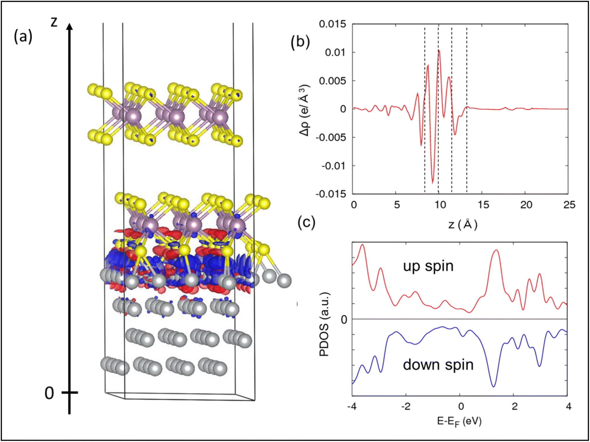
For measuring the structural stabilization and theoretical verification, we have also carried out DFT calculations. The first-principles calculations were performed with the Vienna Ab initio Simulation Package (VASP) code.24 We used the projector augmented wave (PAW) method.25 The Perdew–Burke–Ernzerhof (PBE)26 functional was used for the exchange–correlation functional. The plane-wave energy cut-off was set to 400 eV. The dispersion correction was included via Grimme’s D3(BJ) method.27,28 The Ni–MoS2 interface was constructed by using a hexagonal (cell length along the surface parallel is 9.57 Å) unit cell containing a four-layered Ni(111)-p (4 × 4) slab and two-layered 2H–MoS2-p (3 × 3) slab. Ni is subjected to a small (∼4%) strain to make it commensurate with MoS2. However, this strain does not affect the electronic structure of the Ni (111) surface. The optimized structure is displayed in Fig. 2(a). A 20 Å vacuum was inserted to avoid artificial interaction between slabs. The Brillouin zone was sampled with a Monkhorst–Pack 2 × 2 × 1 k-grid.
 |
| | Fig. 2 (a) Optimized structures of the Ni–MoS2 interface, together with the charge difference plot. The blue and red represent the charge depletion and accumulation regions, respectively. The isosurface value is 0.003 e Bohr−3. (b) xy-Averaged charge difference along the surface-perpendicular (z) direction, i.e. at the interface. The four dashed lines indicate the positions of top Ni, S, Mo, S from the left, respectively. (c) Projected density of states of the interfacial S layer, showing the asymmetric nature due to spin polarization. | |
The charge difference (Fig. 2(a and b)) clearly indicates that the electrons are transferred from the Ni surface to the interfacial S layer. The large electron transfer is supported by the strong binding energy between Ni and MoS2, which was calculated to be −12.1 eV/0.8 nm2. By reflecting the electron transfer at the interface, the projected density of states (PDOS) of the interfacial S layer (Fig. 2(c)) shows a gapless feature. Moreover, the PDOS of the down spin is higher than that of the up spin at the Fermi level, which is similar to the density of states of Ni. The efficiency of the spin polarization, η = (ρ↓ − ρ↑)/(ρ↓ + ρ↑), where ρ↑ and ρ↓ is the density of up and down spins, respectively, is about 15% at the Fermi level. Such a spin-polarized S layer appearing at the interface would contribute to the magnetic response of the Ni–MoS2 composite.
3. Results and discussion
3.1. Spontaneous polarization of negative magnetization states at the hybrid interface
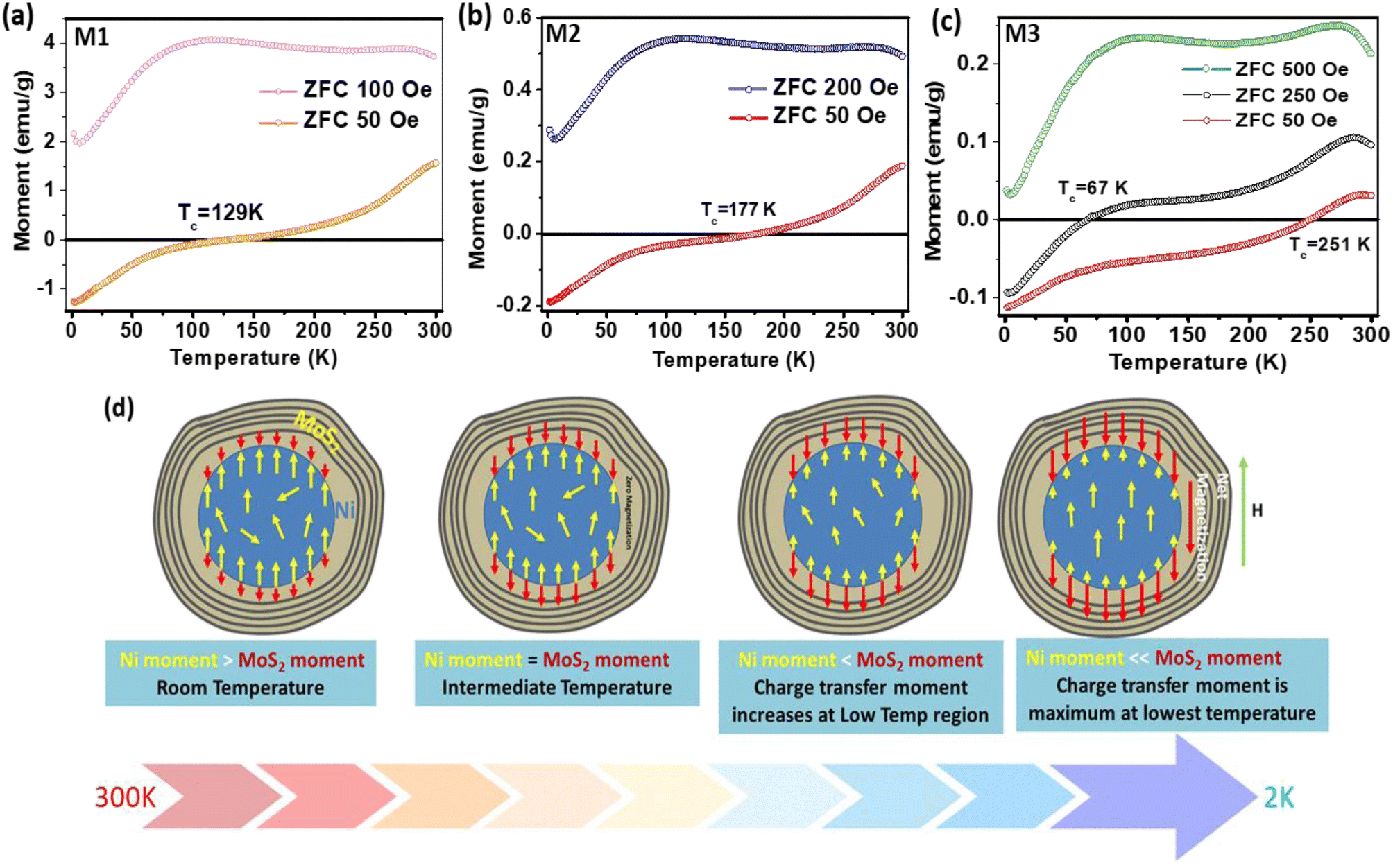
Fig. 3 shows the spontaneous dc magnetization curves of the Ni–MoS2 hybrids in the zero-field cooling (ZFC) process at different magnetic fields in the temperature range of 2–300 K. Interestingly, a spontaneous negative magnetization state is obtained for all three samples in the low-temperature region. Beyond some critical temperature, the net magnetization becomes positive. For ZFC at 50 Oe, these compensation temperatures (Tc) for M1, M2 and M3 are obtained as 129 K, 177 K and 251 K respectively (Fig. 3(a–c)). The negative effect is the strongest for the thinnest layered sample (M3) having the largest Tc. To investigate the effect of a positive dc external field on this negative magnetization, we gradually increased the magnitude of the field, as shown in Fig. 3(a–c). It is observed that in the cases of M1 and M2, this negative magnetization state can be erased with 100 and 200 Oe positive dc fields, respectively (Fig. 3(a and b)). However, for M3, a large 500 Oe dc field is required to change the polarization of magnetization from negative to positive (Fig. 3(c)). In the complete ZFC–FC (FC: field cooling) process, a large exchange splitting is observed with ferromagnetic saturation at low temperature (Fig. S2a ESI†).
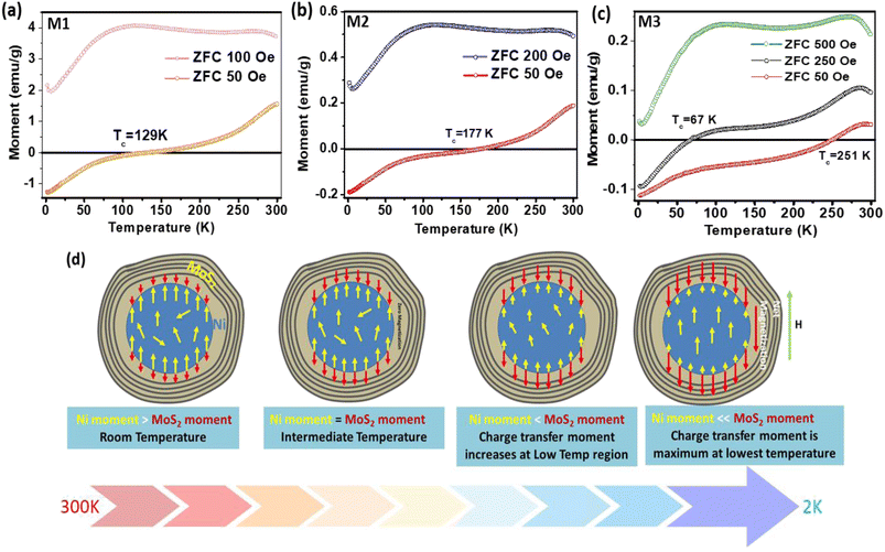 |
| | Fig. 3 Spontaneous magnetization as a function of temperature with various ZFC magnetic fields for (a) M1, (b) M2 and (c) M3 composites. Tc represents the compensation temperature that varies with the samples. (d) Schematic model for change of spin alignment at the interface in the hybrid nanostructure with temperature changes. The magnitudes of the Ni moment and MoS2 moment change with temperature. Red and yellow represent the spin magnetic moments from MoS2 and Ni, respectively. | |
Negative magnetization is sometimes found due to the residual trap field of the superconducting magnet used in the SQUID magnetometer.29,30 To exclude the effect of the trap field, we demagnetized the SQUID coil at 300 K in oscillating mode before each measurement. In addition to that, we also performed a set of experiments with both positive/negative fields and found it was not due to an internal trap field (ESI Fig. S2b†).
3.2. Schematic model for thermal spin orientation at the interface
To explain the observed negative magnetization state in the ZFC process, we have considered a schematic diagram of spin orientation at the interface (Fig. 3(d)). It is known that, due to hybridization between the TM’s 3d orbital and the nearest p orbital of MoS2, a charge transfer occurs from the 3d orbital of the transition metal to the p-orbital of the substrate.1,2,19 During our XPS studies and DFT calculations, we already found this kind of hybridization at the interface. Induction of spin magnetic moments in MoS2 remains antiferromagnetically coupled to Ni spins at the interface.31 Hence, the soft ferromagnetic Ni core is surrounded by an antiferromagnetic 3D shell, formed at the interface of Ni–MoS2. With a change in temperature, the relative orientation of the spin component changes and when they become perfectly antiparallel, the net moment becomes zero (at the compensation temperature, Tc). The details of the spin configuration at different temperatures are explained in the ESI (Section C).† At low temperature, the hybridization due to orbital overlapping is better and the net magnetization is dominated by the charge transfer effect. With a rise in temperature, charge transfer is decreased due to enhanced thermal fluctuation.32–34
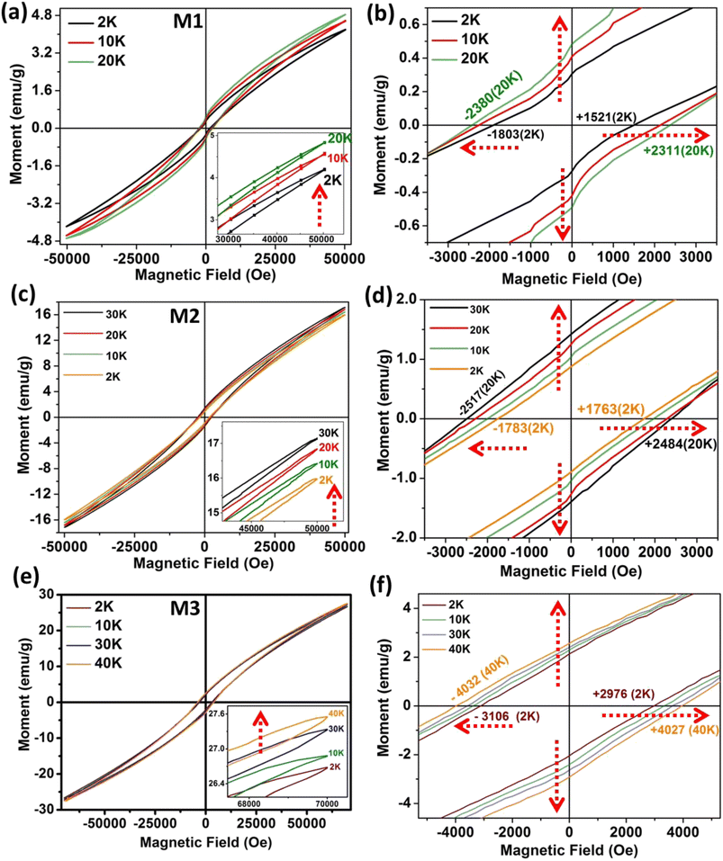
3.3. Anomalous exchange coupling variation with temperature
Interestingly, despite metallic Ni having soft ferromagnetism, the Ni–MoS2 hybrid nanostructure shows very high coercive force and ZFC exchange bias. For Ni nanoparticles, the magnetization saturates at lower fields due to the soft ferromagnetic nature, with much less coercive field, as found in the literature.35,36 In the pristine Ni nanophase, there is also no asymmetry in the coercive field due to the uniformity in the magnetic phase. For a normal magnetic system, coercivity usually decreases with rising temperature, as anisotropy falls more sharply than magnetization with increasing temperature.37–39 With rising temperature, thermal fluctuation destroys the coupling among spins.40–42 However, in this case, it has been found that with increasing temperature, the remanent magnetization and moment increase anomalously. Average coercivity is also enhanced with temperature, which is fundamentally related to memory applications. Fig. 4(a) shows that starting from the lowest temperature of 2 K, the magnetic moment increases up to 20 K for M1. The magnified view (Fig. 4(b)) reveals the clear increment in the coercive field and remanent magnetization with increasing temperature. For M2 and M3, a similar trend is found up to temperatures of 30 K (Fig. 4(c)) and 40 K (Fig. 4(e)), respectively, showing a tunability with changing the Ni core dimensions and MoS2 layer numbers.
 |
| | Fig. 4
M–H hysteresis loops at different temperatures. (a) For M1; inset shows the increasing moment value with temperature. (b) Magnified view for M1 showing increasing coercivity and remanent magnetization with temperature, up to 20 K. (c) M–H loop for M2. (d) Increasing coercivity and remanent magnetization with temperature, up to 30 K. (e) M–H loop for M3. (f) Magnified view shows increasing coercivity and remanent magnetization with temperature, up to 40 K. | |
Due to the large asymmetry in the coercivity, it is pertinent to calculate the average coercivity using the formula Hc = (|Hc+| + |Hc−|)/2, where Hc+ and Hc− are the positive and negative coercive fields (Table 1). Quantitatively, the average coercivities at 2 K were 1662, 1773 and 3041 Oe for M1, M2 and M3, respectively. However, upon increasing the temperature, the coercivities jumped to 2345 Oe (20 K), 2500 Oe (30 K) and 4029 Oe (40 K) for the three samples, respectively, showing further applicability of the large thermoremanent memory effect. The strength of the ZFC exchange bias (HE) is also calculated by considering the polarity of Hc, i.e.: HE = (Hc+ + Hc−)/2, where Hc+ and Hc− are the positive and negative coercive fields, respectively. Since the interface of the hybrid nanostructure contains ferro–antiferromagnetic coupling, we also analysed the field-cooling (FC) M–H loops and evaluated the FC exchange bias as a function of temperature. Table S1 (section D: ESI)† shows the detailed variation of the FC exchange bias with temperature (Fig. S4†). In the ZFC magnetization (Fig. 3(a–c)), we observed a negative magnetization state at low temperature under nominal fields. During the initial magnetization in the M–H loop, in the near-zero-field region we also consistently found the initial moment to be negative (ESI Fig. S5(c, f and e)†) for the three composite samples. However, as the magnitude of the positive field rises, the moment becomes positive. Hence, the spontaneous magnetization behavior (ZFC) and M–H hysteresis are consistent. The origin of magnetization reversal is the competition between charge-transfer-induced magnetization and the inherent ferromagnetic phase, which have different thermal responses. To understand this in a better way, we discuss this part schematically in ESI Fig. S6.†
Table 1 Variation of avg. coercivity and ZFC exchange bias with temperature for all the samples
| M1 |
M2 |
M3 |
|
T (K) |
H
c
+
|
H
c
−
|
Avg. Hc (Oe) |
ZFC exchange bias (Oe) |
T (K) |
H
c
+
|
H
c
−
|
Avg. Hc (Oe) |
ZFC exchange bias (Oe) |
T (K) |
H
c
+
|
H
c
−
|
Avg. Hc (Oe) |
ZFC exchange bias (Oe) |
| 2 |
1521 |
−1803 |
1662 |
−141 |
2 |
1763 |
−1783 |
1773 |
−10 |
2 |
2976 |
−3106 |
3041 |
−65 |
| 10 |
1924 |
−2058 |
1991 |
−67 |
10 |
2167 |
−2290 |
2228.5 |
−61.5 |
10 |
3342 |
−3392 |
3367 |
−25 |
| 20 |
2311 |
−2380 |
2345.5 |
−34.5 |
20 |
2397 |
−2486 |
2441.5 |
−44.5 |
30 |
3630 |
−3642 |
3636 |
−6 |
| 50 |
444 |
−468 |
456 |
−12 |
30 |
2484 |
−2517 |
2500.5 |
−16.5 |
40 |
4027 |
−4032 |
4029.5 |
−2.5 |
| 100 |
233 |
−241 |
237 |
−4 |
50 |
1785 |
−1790 |
1787.5 |
−2.5 |
50 |
3408 |
−3412 |
3410 |
−2 |
| 200 |
195 |
−197 |
196 |
−1 |
100 |
1584 |
−1587 |
1585.5 |
−1.5 |
100 |
1979 |
−1973 |
1976 |
−1.5 |
| 250 |
166 |
−165 |
165.5 |
0.5 |
200 |
727.9 |
−730.5 |
729.2 |
−1.3 |
200 |
1141 |
−1144 |
1142.5 |
−1.5 |
| 300 |
104 |
−94 |
99 |
5 |
300 |
259.81 |
−251.87 |
255.84 |
3.97 |
300 |
221 |
−223 |
222 |
−1 |
3.4. Robust switching effect of magnetization polarization and transient response
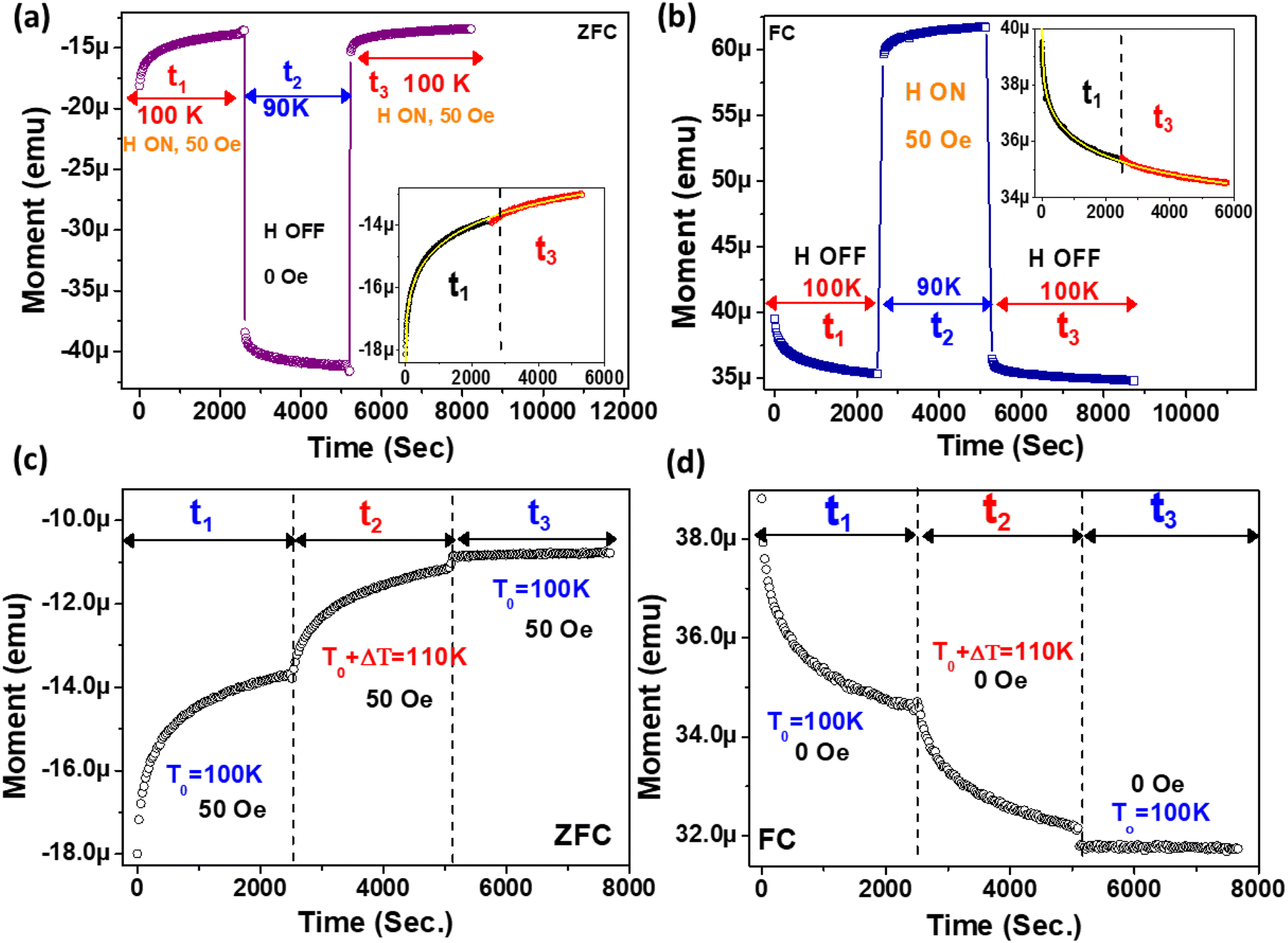
Next, we investigated the switching of magnetic polarization between positive and negative states (Fig. 5(a)). The sample was subjected to ZFC to 1.8 K and then magnetization was started under 50 Oe field. After 200 s, the field was ramped to 200 Oe and accordingly the magnetization also jumped from a negative to positive value instantaneously. The cycle was repeated while the magnetization consistently jumped between the same negative and positive levels. The important outcome is that in contrast to a normal ferromagnetic system, where the magnetization reversal is only possible by changing the polarity of the field, here the switching is achieved only by changing the small-magnitude bias field without changing its polarity. The endurance of the magnetization levels is consistent for long cycles, which promises robustness of the magnetization state. Next, the effect of temperature ramping on the magnetization state is investigated (Fig. 5(b)) via FC (50 Oe) to 1.8 K from 300 K. Here, the instantaneous dc moment is recorded as a function of elapsed time and the temperature is increased after constant time intervals, staying at each temperature step for 600 s. A step-like behaviour with transient response has been obtained and after a certain temperature the magnetization becomes positive. The inset in Fig. 5(b) shows that the steady state is reached quickly, even after a temperature-step change.
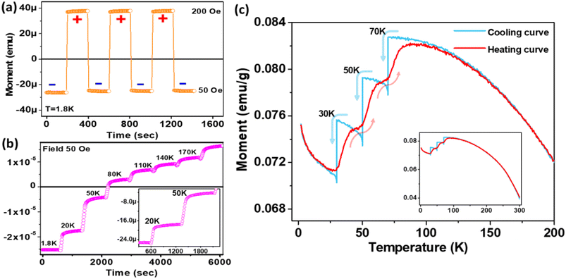 |
| | Fig. 5 (a) Switching polarity of magnetization response with applied field bias. (b) Transient response of magnetization with changing temperature at constant field. (c) Thermoremanent magnetization history, showing the memory effect, and retracing cooling and heating curves at the particular states. The inset shows the full-view curve in the temperature range of 1.8–300 K. | |
3.5. Controlling thermoremanent magnetization in the read/write memory effect
To study the read/write effect of the memory state, we measured FC magnetization via a different protocol. At first, the sample was cooled down from 300 K in a 50 Oe field (rate 3 K min−1), but temporarily kept at 70 K, 50 K and 30 K for a waiting time of 1 h at each temperature, and the magnetic field was switched off to let the magnetization relax downward. After each step, the 50 Oe field was reapplied and the cooling was continued. The purpose of this protocol was to create local steps in the magnetization (writing memory states), shown by the blue curve in Fig. 5(c). After reaching 2 K, temperature is raised again to 300 K, but without halting at any temperature. The magnetization curve obtained during the heating process is shown by the red curve. The interesting outcome is that the return magnetization also traces the exact same path, i.e., with a step-like behaviour at particular temperatures, although no wait time was given during heating. Hence, the sample can remember its temperature-based magnetization states. In contrast to an applied bias field, which is the conventional memory-controlling parameter, here thermal treatment is used as an extra parameter for creating memory states.
3.6. Modelling of relaxation dynamics using correlation parameters
To investigate the role of temperature and field in controlling the memory state, we have carried out dc long relaxation measurements, using both ZFC and FC methods. Details about this measurement protocol are given in the ESI (Section F).†Fig. 6(a) shows the ZFC relaxation curve measured in this protocol. As soon as the magnetic field is turned on, the moment starts to grow exponentially, up to time t1. In the intermediate time t2, when the temperature is changed to 90 K (temporary cooling: T0 − ΔT), the moment level changes and continues to relax independently. But, as soon as the temperature is retraced back to T0, the magnetization level returns back to the same value before temporary cooling. The moment continues to relax along the field direction exponentially, similar to t1, during the whole time interval of t3. The inset (Fig. 6(a)) verifies that relaxation during t3 is an extension of the curve during t1 and is totally independent of the forced temporary cooling t2. To understand the magnetization as a function of time, we have used a stretched exponential function, as follows:43| |  | (1) |
Here, M0 is the ferromagnetic component, Mr is the remanent part and τ is the relaxation time. β is known as the stretching parameter and lies between 0 and 1. The β value 0 implies a constant magnetization, i.e., no relaxation at all, and β = 1 signifies a single time constant, i.e., a very strong relaxation.44 To distinguish the relaxation behaviour from two components due to the hybrid structure, we have considered contributions from two spin origins (‘Ni’ spin and MoS2 ‘S’ spin) that are antiferromagnetically correlated. During the time interval of t1, both the spins relax under the magnetic field, and we have decoupled the relaxation function in eqn (1) as a function of the separate relaxation time, interaction parameter and remanent component:| | 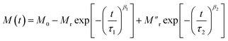 | (2) |
where τ1, β1 and τ2, β2 are the relaxation times and exponents for the ‘Ni’ and ‘MoS2’ spins, respectively. The remanent component Mr is also changed accordingly. In the first interval t1 we used eqn (2) for the ZFC case (Fig. 6(b)). The fitted parameters show an important result about the relaxation process (Table 2). It is found that the relaxation time of the ‘Ni’ spin (τ1 = 97.6 s) is much less than that of the ‘MoS2’ spin (τ2 = 1510 s). This is because Ni remains soft ferromagnetic and as a result, the response of the core ‘Ni’ spin to magnetic field is much faster than that of the ‘MoS2’ spin residing at the interface. The lower β value of the Ni spin (β1 = 0.34) compared to that of ‘MoS2’ spin (β2 = 0.43) also indicates better exchange coupling among the ‘Ni’ spins compared to ‘MoS2’.
 |
| | Fig. 6 (a) Time evolution of magnetization memory in ZFC with temporary cooling. The inset shows continuous fitting of t3 and t1. (b)–(d) Variation of relaxation at the time intervals of t1, t2, and t3 respectively. The solid red lines are the theoretically fitted curves. (e) Relaxation of magnetization memory in FC with temporary cooling. The inset shows that t3 is a continuation of t1. (f)–(h) Variation of relaxation at the time intervals of t1, t2, and t3 respectively. The solid red lines are the curves fitted with the corresponding equations. | |
Table 2 Relaxation parameters obtained after fitting with eqn (2) and (3) for the ZFC case
| Parameters for the ZFC case |
t
1 (0–2000 s) |
t
3 (4000–7000 s) |
Parameters |
t
2 (2000–4000 s) |
| Value |
Std. error ± |
Value |
Std. error ± |
Value |
Std. error ± |
|
M
0 (emu) |
−1.33 × 10⁻⁵ |
7.94 × 10⁻⁸ |
−1.23 × 10⁻⁵ |
7.25 × 10⁻⁷ |
M
0 (emu) |
−1.43 × 10⁻⁵ |
1.41 × 10⁻⁶ |
|
M
r (emu) |
9.51 × 10⁻⁶ |
5.66 × 10⁻⁷ |
5.28 × 10⁻⁶ |
1.76 × 10⁻⁷ |
M
r (emu) |
5.79 × 10⁻⁶ |
7.22 × 10⁻⁷ |

|
4.33 × 10⁻⁶ |
5.74 × 10⁻⁸ |
5.97 × 10⁻⁷ |
1.56 × 10⁻⁸ |

|
1.23 × 10⁻⁶ |
1.03 × 10⁻⁷ |
|
β
1
|
0.34 |
0.0023 |
0.38 |
0.0021 |
β
3
|
0.93 |
0.0035 |
|
β
2
|
0.43 |
0.0094 |
0.44 |
0.0129 |
β
4
|
0.34 |
0.0023 |
|
τ
1 (s) |
97 |
4 |
83 |
5 |
τ
3 (s) |
154 |
6 |
|
τ
2 (s) |
1510 |
12 |
1653 |
17 |
τ
4 (s) |
65 |
4 |
Next, during t2, the reduced temperature (T0 − ΔT) causes two different effects on the ‘Ni’ and ‘MoS2’ spins. In the case of the ‘MoS2’ spin, two opposing effects are involved, one being the original component of field relaxation in the direction of the applied field and the other a reduced temperature effect which tries to increase the moment opposite to the external field due to an interfacial ‘negative magnetization’ effect. Because of these opposing effects in ‘MoS2’, we considered only the true relaxation of ‘Ni’ spins during t2. Here, the two relaxation parts are the temperature change contribution and normal field relaxation. The equation is similar, the parameters are just indexed differently.
| | 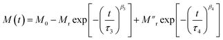 | (3) |
The first part corresponds to the temperature contribution (τ3, β3) and the second part (τ4, β4) represents the normal field relaxation. The data during t2 are fitted well by eqn (3) (Fig. 6(c) and Table 2). Finally, during t3, the temperature is returned to 100 K and accordingly the moment decreases with increasing thermal anisotropy. The t3 curve is also fitted using eqn (2) considering the field relaxation processes of the ‘Ni’ and ‘MoS2’ spins (Fig. 6(d) and Table 2). Interestingly, the fitted relaxation parameters are very similar to those obtained during t1, indicating preservation of thermal memory.
During FC relaxation (Fig. 6(e)), the results are very similar and consistent with the ZFC case. Thus, in the ZFC and FC cases, the state of the magnetic system before temporary cooling is retraced as soon as the temperature returns to its initial value, i.e., the memory effect is verified in the Ni–MoS2 hybrid nanostructure. Here, we have also checked the fitting of data in t1 and t3 with eqn (2), as shown in Fig. 6(f–h). The parameters are given in Table 3.
Table 3 Parameters obtained after fitting with eqn (2) and (3) for the FC case
| Parameters for the FC case |
t
1 (0–2500 s) |
t
3 (5000–8800 s) |
Parameters |
t
2 (2500–5000 s) |
| Value |
Std. error ± |
Value |
Std. error ± |
Value |
Std. error ± |
|
M
0 (emu) |
3.18 × 10⁻⁵ |
6.46 × 10⁻⁷ |
3.24 × 10⁻⁵ |
3.86 × 10⁻⁷ |
M
0 (emu) |
3.28 × 10⁻⁵ |
1.92 × 10⁻⁷ |
|
M
r (emu) |
−5.21 × 10⁻⁶ |
1.29 × 10⁻⁸ |
−4.89 × 10⁻⁶ |
2.34 × 10⁻⁷ |
M
r (emu) |
−1.86 × 10⁻⁶ |
3.44 × 10⁻⁷ |

|
3.22 × 10⁻⁷ |
2.43 × 10⁻⁸ |
4.24 × 10⁻⁶ |
3.23 × 10⁻⁷ |

|
1.54 × 10⁻⁶ |
2.58 × 10⁻⁷ |
|
β
1
|
0.30 |
0.0678 |
0.32 |
0.0057 |
β
3
|
0.29 |
0.0137 |
|
β
2
|
0.44 |
0.0353 |
0.46 |
0.0041 |
β
4
|
0.56 |
0.0032 |
|
τ
1 (s) |
110 |
4 |
139 |
11 |
τ
3 (s) |
1352 |
12 |
|
τ
2 (s) |
1483 |
15 |
1562 |
23 |
τ
4 (s) |
156 |
5 |
3.7. Simultaneous effect of field switching ON/OFF and temperature on the magnetization memory state
To measure the strength of the memory state, we have performed another series of magnetizations where the system is allowed to undergo opposite forced relaxations by switching the applied magnetic field OFF/ON during the temporary cooling time t2 (Fig. 7). During temporary cooling, we have deliberately set the magnetic field [on/off] to forcefully relax the system at lower temperature for stronger jumps. It is evident that the magnetization value shows a large dip with relaxation in the opposite direction due to field switching (Fig. 7(a and b)). It is interesting to note that, even after such a large opposite relaxation at 90 K, the magnetization value quickly reaches the level that it would have reached before the temporary cooling when the same temperature and field conditions are restored. In this case also, despite the changes in field and temperature, the relaxation curves t1 and t3 can be continuously fitted. Therefore, these experiments confirm the robustness of the memory effect in the hybrid with large thermal and field ramping.
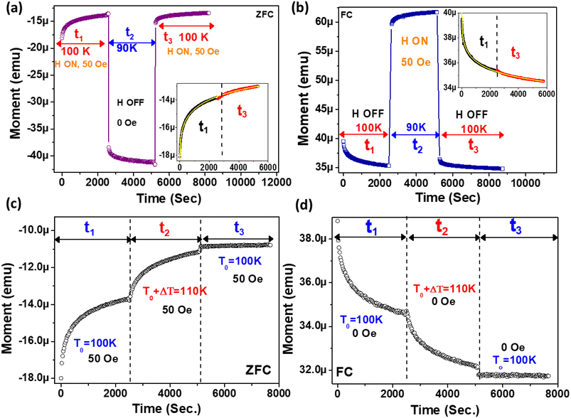 |
| | Fig. 7 (a and b) Forced relaxations with simultaneous temperature and field changes for (a) the ZFC method and (b) the FC method. The inset shows that t3 is a continuation of t1 fitted with eqn (1), even after a large jump. (c and d) Magnetic relaxation with positive thermal cycling for (c) the ZFC method and (d) the FC method. Reinitialization of the memory state occurs with ΔT positive thermal cycling. Here, t3 is not a continuation of t1. | |
3.8. Re-initialization of the memory state
Next, to erase the memory state, positive thermal cycling has been used as a parameter. After ZFC to T0 = 100 K, a magnetic field of 50 Oe is applied with a consequent magnetization of 2500 s (t1) (Fig. 7(c)).
After t1, the sample is quickly heated to a temperature of T0 + ΔT = 110 K, followed by magnetization for t2 = 2500 s. Next, the sample is finally quenched to T0 = 100 K and measurements continued for 2500 s (t3). Here, the contrasting difference is that, unlike temporary cooling, the magnetization at the beginning of the t3 cycle does not come to the same level as it was before temporary heating. Also, the nature of magnetization relaxation during t3 is completely different from that during t1. In the FC cycle, deletion of memory has also been found (Fig. 7(d)). The important outcome is that, upon temporary heating by ΔT, the magnetization state is refreshed. Therefore, to delete the memory state, one has to just increase the temperature by a small amount to re-initialize the system.
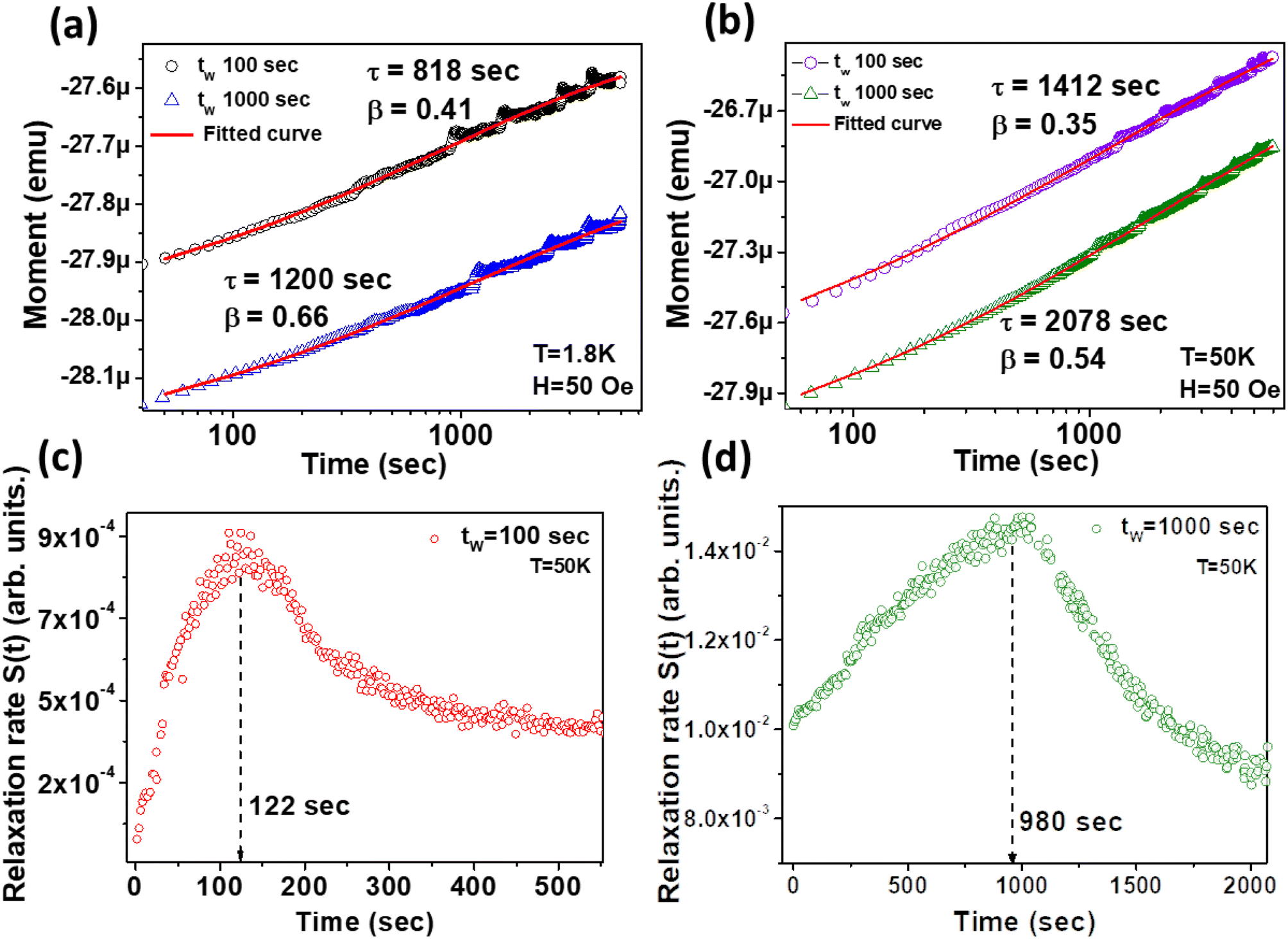
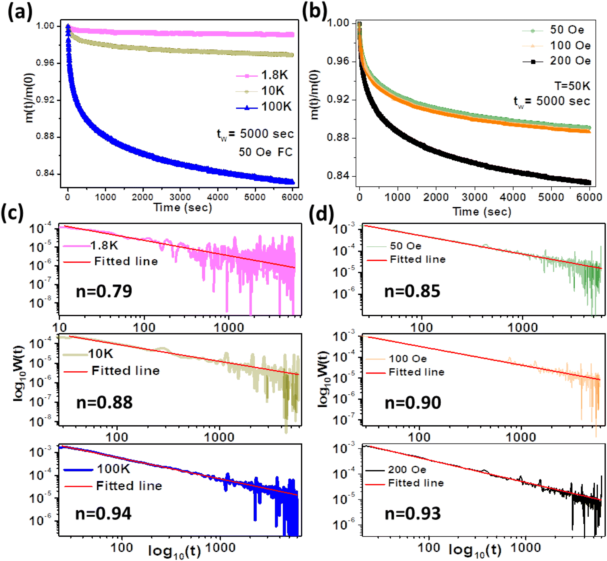
3.9. The role of ageing effects and wait-time dependence
Since the occurrence of memory establishment is always related to ageing effects for longer storage of information, it is pertinent to measure different wait-time dependences (tw = 100 s, 1000 s) before starting measurement. A wait time is applied for thermal stabilization of the memory states. After tw, a 50 Oe dc magnetic field is applied and the time evolution of magnetization is recorded (Fig. 8(a) and (b)).
 |
| | Fig. 8 (a and b) Wait-time dependence and thermal stabilization effect on magnetic relaxation at (a) 1.8 K and (b) 50 K, using the 50 Oe ZFC method in both the cases. The solid red lines are the curves fitted with eqn (1). (c and d) The relaxation rate S(t) vs. time plot at two different wait times, (c) tW = 100 s and (d) tW = 1000 s, exhibiting the ageing behaviour. The peak position in the curve is shown by the dashed line. | |
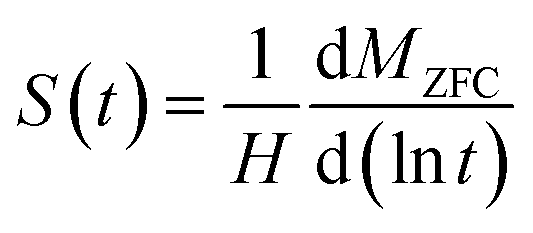
In eqn (1), Mr, τ (characteristic relaxation time) and β (stretching parameter) are proportionate functions of temperature and wait time tw, respectively. τ increases with large tw due to stiffening of spin relaxation. The ESI (section H)† describes the variation of τ and β with tw in detail. The ageing effect can be understood in a better way by evaluating the relaxation rate S(t), which is obtained from the logarithmic time derivative of the ZFC susceptibility as follows:45
| | 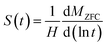 | (4) |
where
MZFC is the magnetization with application of wait time. The relaxation rates
S(
t) are shown in
Fig. 8(c) and (d). The important fact from the relaxation curves is that if the magnetization has wait-time dependence, then a point of inflection should be found at an observation time closely equal to the wait time
tw, which has been observed in this case. The point of inflection (maximum of
S(
t)) shifts to a longer observation time when increasing the wait time from 100 s to 1000 s.
Next, we find the decay of the remanent magnetization (memory) rate using a theoretical model given by Ulrich et al.46 Based on this model, the remanent magnetization rate can be defined as
| | 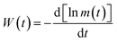 | (5) |
m(
t) is the temperature dependent magnetization.
This magnetization rate decays during the FC thermoremanence measurements and the nature of the variation can be fitted using a power law, such as:
| | | W(t) = At−n, for t ≥ t0 | (6) |
where
t0 is known as the cross-over time,
A is a constant and the exponent
n is a function of temperature and field.
n defines the strength of interaction at the interface. The protocol for this particular thermoremanent magnetization (TRM) can be found in the ESI (section I).
† TRM measurements at different temperatures and fields are carried out for a wait time of 5000 s (
Fig. 9(a and b)). The relaxation rate is fitted with
eqn (6) after a cross-over time of
t0 ≈ 50 s. The value of
n is found to have a functional dependence on temperature and field and the parameters are tabulated in Table SII (ESI).
† The dependency can be seen in
Fig. 9(c and d). The decay rate is the slowest at low temperature (1.8 K) due to strong interaction among the spins, while the decay rate is faster at 100 K due to high thermal agitation. From thermal and field variation treatments, it could be estimated that the operation of this hybrid system under extreme ramping conditions is possible. Faster decay at higher FC magnetic fields signifies that a large number of magnetization states were registered in the system at high magnetic fields.
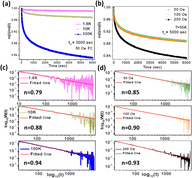 |
| | Fig. 9 Variation of normalized FC magnetization at (a) different temperatures and (b) different magnetic fields. (c) Relaxation-rate plots at different temperatures. (d) Relaxation-rate plots at different fields. The straight lines are the linear fits with eqn (6). | |
4. Conclusion
In summary, a nested Ni nanostructure is grown on a MoS2 surface and subsequently wrapped by it under feasible synthetic control. By tuning the number of layers of MoS2 and the charge transfer effect at the interface, a negative magnetization state with antiferromagnetic coupling has been established due to uncompensated spin components formed at the boundary. DFT calculations show a spin-polarized DOS at the interface. A giant enhancement in coercivity with high exchange bias, which anomalously increases with temperature, is explained on the basis of the interaction picture. Generation of a large coercive field predicts the possibility of robust memory applications and different relaxation measurements reveal a thermoremanent memory state that can be probed via temperature and field. Long relaxation measurements under a unique protocol indicate the sturdiness and endurance of the hybrid system for future practical applications. For 2D-based systems, this type of thermoremanent memory effect is newly observed. We believe that this material, with high exchange bias, will be useful in fabricating temperature-based nanomagnetic memory devices.
Conflicts of interest
There are no conflicts to be declared by all the authors.
Acknowledgements
S. B. acknowledges the Japan Society for the Promotion of Science for providing a JSPS Postdoctoral Fellowship (ID P20070 standard). S. K. S acknowledges the DST, Govt. of India and IACS for providing infrastructural support. H. T acknowledges funding from Grant-in-Aid for JSPS Research Fellows (KAKENHI, project numbers 22H00315, 22F20070 and 22KF0237) during this work. T. O. acknowledges JST-PRESTO Grant Number JPMJPR2115.
References
- S. Bhattacharya, D. Dinda, B. K. Shaw, S. Dutta and S. K. Saha, Phys. Rev. B, 2016, 93, 184403 CrossRef.
- S. Bhattacharya, E. M. Kumar, R. Thapa and S. K. Saha, Appl. Phys. Lett., 2017, 110, 032404 CrossRef.
- C. Majumder, S. Bhattacharya and S. K. Saha, Phys. Rev. B, 2019, 99, 045408 CrossRef CAS; A. Debnath, B. K. Shaw, S. Bhattacharya and S. K. Saha, J. Phys. D: Appl. Phys., 2021, 54(20), 205001 CrossRef.
- L. Neel, Ann. Phys., 1948, 12, 137 Search PubMed.
- H. Shen, Z. X. Cheng, F. Hong, J. Y. Xu, J. Y. Xu, S. J. Yuan, S. X. Cao and X. L. Wang, Appl. Phys. Lett., 2013, 103, 192404 CrossRef.
- Y. Ren, T. T. M. Palstra, D. I. Khomskii, E. Pellegrin, A. A. Nugroho, A. A. Menovsky and G. A. Sawatzky, Nature, 1998, 396, 441 CrossRef CAS.
- K. Yoshii, Mater. Res. Bull., 2012, 47, 3243 CrossRef CAS.
- K. Yoshii and A. Nakamura, J. Solid State Chem., 2000, 155, 447 CrossRef CAS.
- Y. Sun, M. B. Salamon, K. Garnier and R. S. Averback, Phys. Rev. Lett., 2003, 91, 167206 CrossRef PubMed.
- G. M. Tsoi, L. E. Wenger, U. Senaratne, R. J. Tackett, E. C. Buc, R. Naik, P. P. Vaishnava and V. Naik, Phys. Rev. B: Condens. Matter Mater. Phys., 2005, 72, 014445 CrossRef.
- S. Bhattacharya, W. Choi, A. Ghosh, S. Lee, G. D. Lee and S. K. Kim, Nanotechnology, 2021, 32, 385705 CrossRef CAS PubMed.
- M. Sasaki, P. E. Jonsson, H. Takayama and H. Mamiya, Phys. Rev. B: Condens. Matter Mater. Phys., 2005, 71, 104405 CrossRef.
- D. Liang, Y. Zhang, P. Lu and Z. G. Yu, Nanoscale, 2019, 11, 18329–18337 RSC.
- D. Wang, X. Zhang, Y. Shena and Z. Wu, RSC Adv., 2016, 6, 16656–16661 RSC.
- X. Hanab, M. Benkraouda, N. Qamhieha and N. Amrane, Chem. Phys., 2020, 528, 110501 CrossRef.
- L. M. Martinez, J. A. Delgado, C. L. Saiz, A. Cosio1, Y. Wu, D. Villagrán, K. Gandha, C. Karthik, I. C. Nlebedim and S. R. Singamaneni, J. Appl. Phys., 2018, 124, 153903 CrossRef.
- R. Tenne, Adv. Mater., 1995, 7, 965 CrossRef CAS.
- J. Etzkorn, H. A. Therese, F. Rocker, N. Zink, U. Kolb and W. Tremel, Adv. Mater., 2005, 17, 2372–2375 CrossRef CAS; A. N. Enyashin, S. Gemming, M. Bar-Sadan, R. Popovitz-Biro, S. Hong, Y. Prior, R. Tenne and G. Seifert, Angew. Chem., Int. Ed., 2007, 46, 623 CrossRef PubMed.
- X. Liu, C. Z. Wang, Y. X. Yao, W. C. Lu, M. Hupalo, M. C. Tringides and K. M. Ho, Phys. Rev. B: Condens. Matter Mater. Phys., 2011, 83, 235411 CrossRef.
- K. Pi, K. M. McCreary, W. Bao, W. Han, Y. F. Chiang, Y. Li and R. K. Kawakami, Phys. Rev. B: Condens. Matter Mater. Phys., 2009, 80(7), 075406 CrossRef CAS; A. Debnath, S. Bhattacharya and S. K. Saha, J. Phys. D: Appl. Phys., 2020, 53(22), 225004 CrossRef; X. H. Huang, J. F. Ding, G. Q. Zhang, Y. Hou, Y. P. Yao and X. G. Li, Phys. Rev. B: Condens. Matter Mater. Phys., 2008, 78, 224408 CrossRef; T. J. Park, G. C. Papaefthymiou, A. J. Viescas, Y. Lee, H. Zhou and S. S. Wong, Phys. Rev. B: Condens. Matter Mater. Phys., 2010, 82, 024431 CrossRef.
- R. Tenne, Angew. Chem., Int. Ed., 2003, 42, 5124–5132 CrossRef CAS PubMed.
- N. Sano,
et. al.
, Chem. Phys. Lett., 2003, 368, 331 CrossRef CAS.
- A. Zak,
et. al.
, J. Am. Chem. Soc., 2000, 122, 11108 CrossRef CAS.
- G. Kresse and J. Hafner, J. Phys.: Condens. Matter, 1994, 6, 8245 CrossRef CAS.
- P. E. Blöch, Phys. Rev. B: Condens. Matter Mater. Phys., 1994, 50, 17953–17979 CrossRef PubMed.
- J. P. Perdew, K. Burke and M. Ernzerhof, Phys. Rev. Lett., 1996, 77, 3865–3868 CrossRef CAS PubMed.
- S. Grimme, J. Antony, S. Ehrlich and H. Krieg, J. Chem. Phys., 2010, 132, 154104 CrossRef PubMed.
- S. Grimme, S. Ehrlich and L. Goerigk, J. Comput. Chem., 2011, 32, 1456–1465 CrossRef CAS PubMed.
- X. Xie, H. Che, H. Wang, G. Lin and H. Zhu, Inorg. Chem., 2018, 57, 175–180 CrossRef CAS PubMed.
- N. Kumar and A. Sundaresan, Solid State Communications, 2010, 150, 1162–1164 CrossRef CAS; L. D. Tung, Phys. Rev. B: Condens. Matter Mater. Phys., 2006, 73, 024428 CrossRef.
- A. J. Akhtar, A. Gupta, D. Chakravorty and S. K. Saha, AIP Adv., 2013, 3, 072124 CrossRef.
- S. Bag, S. Bhattacharya, D. Dinda, M. V. Jyothirmai, R. Thapa and S. K. Saha, Phys. Rev. B, 2018, 98, 014109 CrossRef CAS.
- A. Debnath, S. Bhattacharya, T. Kumar Mondal, H. Tada and S. K. Saha, J. Appl. Phys., 2020, 127, 013901 CrossRef CAS.
- S. Bhattacharya, D. Dinda, E. M. Kumar, R. Thapa and S. K. Saha, J. Appl. Phys., 2019, 125, 233904 CrossRef.
- X. He,
et al.
, Nanoscale Res. Lett., 2013, 8, 446 CrossRef PubMed.
- M. Reza, A. V. Soltaninejad and M. Ali, Sci. Rep., 2020, 10, 12627 CrossRef PubMed.
- E. Fertman, S. Dolya, V. Desnenko, L. A. Pozhar, M. Kajnakova and A. Feher, J. Appl. Phys, 2014, 115, 203906 CrossRef; X. H. Huang, J. F. Ding, G. Q. Zhang, Y. Hou, Y. P. Yao and X. G. Li, Phys. Rev. B: Condens. Matter Mater. Phys., 2008, 78, 224408 CrossRef.
- J. F. Qian, A. K. Nayak, G. Kreiner, W. Schnelle and C. Felser, J. Phys. D: Appl. Phys., 2014, 47, 305001 CrossRef; T. J. Park, G. C. Papaefthymiou, A. J. Viescas, Y. Lee, H. Zhou and S. S. Wong, Phys. Rev. B: Condens. Matter Mater. Phys., 2010, 82, 024431 CrossRef.
- H. Lin, F. Yan, C. Hu, Q. Lv, W. Zhu, Z. Wang, Z. Wei, K. Chang and K. Wang, ACS Appl. Mater. Interfaces, 2020, 12, 43921 CrossRef CAS PubMed.
- W. Zhu, H. Lin, F. Yan, C. Hu, Z. Wang, L. Zhao, Y. Deng, Z. R. Kudrynskyi, T. Zhou, Z. D Kovalyuk, Y. Zheng, A. Patanè, I. Žutić, S. Li, H. Zheng and K. Wang, Adv. Mater, 2021, 33, 2104658 CrossRef CAS PubMed; C. Majumder, S. Bhattacharya and S. K. Saha, J. Mag. and Mag. Mat., 2020, 506, 166601 CrossRef.
- W. Zhu, S. Xie, H. Lin, G. Zhang4, H. Wu, T. Hu, Z. Wang, X. Zhang, J. Xu, Y. Wang, Y. Zheng, F. Yan, J. Zhang, L. Zhao, A. Patanè, J. Zhang, H. Chang and K. Wang, Chin. Phys. Lett., 2022, 39, 128501 CrossRef.
- S. Bhattacharya and S. K. Saha, Macromol. Symp., 2017, 376(1), 1600183 CrossRef.
- N. Khan 1, P. Mandal 1 and D. Prabhakaran, Phys. Rev. B: Condens. Matter Mater. Phys., 2014, 90, 024421 CrossRef.
- Y. Sun, M. B. Salamon, K. Garnier and R. S. Averback, Phys. Rev. Lett., 2003, 91, 167206 CrossRef PubMed.
-
I. A. Campbell and C. Giovannella, in Relaxation in Complex Systems and Related Topics, Plenum, New York, 1990, p. 3 Search PubMed.
- M. Ulrich, J. Garcıa-Otero, J. Rivas and A. Bunde, Phys. Rev. B: Condens. Matter Mater. Phys., 2003, 67, 024416 CrossRef.
|
| This journal is © The Royal Society of Chemistry 2024 |
Click here to see how this site uses Cookies. View our privacy policy here. 
 Open Access Article
 This Open Access Article is licensed under a Creative Commons Attribution-Non Commercial 3.0 Unported Licence
 ab,
Tatsuhiko
Ohto
ab,
Tatsuhiko
Ohto