
Full automation of point defect detection in transition metal dichalcogenides through a dual mode deep learning algorithm†
Dong-Hwan
Yang‡
 ab,
Yu-Seong
Chu‡
c,
Odongo Francis Ngome
Okello
a,
Seung-Young
Seo
a,
Gunho
Moon
ab,
Kwang Ho
Kim
d,
Moon-Ho
Jo
ab,
Dongwon
Shin
e,
Teruyasu
Mizoguchi
h,
Sejung
Yang
*f and
Si-Young
Choi
*abg
ab,
Yu-Seong
Chu‡
c,
Odongo Francis Ngome
Okello
a,
Seung-Young
Seo
a,
Gunho
Moon
ab,
Kwang Ho
Kim
d,
Moon-Ho
Jo
ab,
Dongwon
Shin
e,
Teruyasu
Mizoguchi
h,
Sejung
Yang
*f and
Si-Young
Choi
*abg
aDepartment of Materials Science and Engineering, Pohang University of Science and Technology (POSTECH), 77 Cheongam-Ro, Pohang 37673, Republic of Korea. E-mail: youngchoi@postech.ac.kr
bCenter for van der Waals Quantum Solids, Institute of Basic Science (IBS), 77 Cheongam-Ro, Pohang 37673, Republic of Korea
cDivision of Biomedical Engineering, College of Health Sciences, Yonsei University, 1, Yeonsedae-gil, Heungeop-myeon, Wonju-si, Gangwon-do, 26493, Republic of Korea
dDepartment of Materials Science and Engineering, Pusan National University (PNU), 2, Busandaehak-ro 63beon-gil, Geumjeong-gu, 46241, Busan, Republic of Korea
eMaterials Science and Technology Division, Oak Ridge National Laboratory (ORNL), Oak Ridge, TN 37831, USA
fDepartment of Precision Medicine, Yonsei University Wonju College of Medicine, 20, Ilsan-ro, Wonju-si, Gangwon-do, Republic of Korea. E-mail: syang@yonsei.ac.kr
gDepartment of Semiconductor Engineering, Pohang University of Science and Technology (POSTECH), 77 Cheongam-Ro, Pohang, 37673, Republic of Korea
hInstitute of Industrial Science, The University of Tokyo, 4-6-1 Komaba, Meguro, Tokyo 15308505, Japan
First published on 22nd November 2023
Abstract
Point defects often appear in two-dimensional (2D) materials and are mostly correlated with physical phenomena. The direct visualisation of point defects, followed by statistical inspection, is the most promising way to harness structure-modulated 2D materials. Here, we introduce a deep learning-based platform to identify the point defects in 2H-MoTe2: synergy of unit cell detection and defect classification. These processes demonstrate that segmenting the detected hexagonal cell into two unit cells elaborately cropped the unit cells: further separating a unit cell input into the Te2/Mo column part remarkably increased the defect classification accuracies. The concentrations of identified point defects were 7.16 × 1020 cm2 of Te monovacancies, 4.38 × 1019 cm2 of Te divacancies and 1.46 × 1019 cm2 of Mo monovacancies generated during an exfoliation process for TEM sample-preparation. These revealed defects correspond to the n-type character mainly originating from Te monovacancies, statistically. Our deep learning-oriented platform combined with atomic structural imaging provides the most intuitive and precise way to analyse point defects and, consequently, insight into the defect-property correlation based on deep learning in 2D materials.
New conceptsWe demonstrated a convolutional neural network (CNN)-based deep learning platform to examine the point defects in monolayer 2H-MoTe2, and associate the “point defects”-“origin of electric properties exhibition” in statistical manners. To achieve these goals, we designed dual mode strategies to improve the accuracy for point defect examination; (i) unit cell detection and (ii) point defect classification in the “unit cell-level”. Recently, a fully convolutional network (FCN) was adopted to define point defects in the “pixel-level”; however, based on our demonstration, the FCN confuses the defect type even in one-species. Moreover, further determination of the point defect type should be conducted by an analyst. We trained one CNN-model to detect a “hexagonal cell” followed by “unit cell-cropping” and the other CNN-model to classify defect types in a unit cell; by comparing classification competence for “a unit cell-input” and “separated unit cell-input into two-parts”. Our approach remarkably increased the unit cell detection and defect classification accuracies, by “dividing analysis process or target-elements” in each step with limited image features of the unit cell. Moreover, we suggested solutions for current limitation to apply deep learning to materials science, mimicking the experimental conditions with simulated training images and accumulation of ground truth within the lack of ground truth in microscopic research fields. |
Introduction
Atomic-level defects such as vacancies, edges, and grain boundaries often appear in two-dimensional (2D) materials. Given that the specific surface area of 2D materials is large, the physical properties become more sensitive to defects.1 Therefore, there have been many efforts to harness defects as a key parameter to manipulate various properties, such as electric,2–15 magnetic,16–25 or thermoelectric.26–29 Specifically, sulfur vacancies in 2H-MoS2 generated during sample preparation by cleavage from bulk 2H-MoS2 act as electron donors: electrons are captured close to the vacancy sites. It was revealed that electrons localised near vacancies govern electric hopping by transport measurements.5 Furthermore, it was reported that a hydrogen (H) atom doped on graphene removes a single pz orbital from two opposite pz orbitals, that is, from sp2 to sp3 orbital states. This polarised orbital system leads to spin-polarised electron states, where a net magnetic moment appears near the H atom.23 For higher defect-dimensions, graphene/hexagonal boron nitride (h-BN) defective interfaces generated during chemical vapour deposition (CVD) relieve the lattice mismatch strain. These defective interfaces (non-hexagonal connections between graphene and h-BN) promote phonons and consequently improve thermoelectric transport, whereas perfect hexagonal interfaces are clamped by residual strain.26These imperfections often guide us to comprehend and, thereby, modulate new functionalities of 2D materials.30,31 Such properties can be predominantly influenced by localised defects;30–33 therefore, in-depth exploration of local atomic defects suggest insights for defect-engineering.30,31 Point defects are the most frequently studied among defect structures, because other types of defects are, in fact, composed of various point defects, serving a key role in correlating defect-structural units.32,33 Besides, point defects, such as vacancies, interstitials, and adatoms on the surface of 2D materials, can be readily generated. Especially in transition metal dichalcogenides (TMDCs), electric properties by point defects can be feasibly modulated due to their high level of structural complexity and relatively weak bonding between transition metals and chalcogens, compared with graphene or h-BN.2,4,34 For instance, n-type pristine 2H-MoTe2 can be manifested to p-type semiconductors by illuminating with a specific laser wavelength.35 These controllable electric properties dominantly originated from vacancies and adatoms adsorbed at vacancy sites.36–38
Atomic-level visualisation via scanning transmission electron microscopy (STEM) is the most-promising strategy to comprehend point defects in 2D materials.39–41 To date, point defects have been visualised and then analysed by recognising the difference between the (i) experimental and (ii) ideal atomic-contrast generated by image simulations.42,43 However, this manual point defect identification represents a labour-intensive burden on analysts. In the field of image recognition e.g. image classification/segmentation and object detection, a convolutional neural network (CNN)-based deep learning analysis platform has been actively adopted and shows high performance.44–46 Recently, a fully convolutional network (FCN)-based encoder-decoder was employed to identify point defect species.47,48 Using the FCN, the recognition process can proceed in two steps: (i) an input image is convoluted by a series of kernels to extract image features i.e., background, host atoms, or defect sites, and (ii) based on the extracted features, the image is deconvoluted to reconstruct the image to the identical size as the input. By applying the FCN to point defect analysis of TMDCs,49,50 the different atomic contrasts/configurations of transition metals or chalcogens are explored to identify point defects.
Since FCN predicts defective sites at pixel-by-pixel, the final defect-type-determination should be verified by humans; this is because one atomic-defect site contains several-pixels in an atomic-structural image. The accurate unit cell detection is the first-phase of point defect analysis in a material, to categorise the defect species. When a human identifies point defects, one may scan it either (i) atom-by-atom or (ii) (extended to) unit cell-by-unit cell, not pixel-by-pixel. Then, one may determine the point defect species by recognising atomic contrast in a unit cell i.e., both chalcogenide (Ch) on-site and transition metal (TM) on-site atomic contrasts. Furthermore, only Ch-on site defect consideration may not discern the VCh (Ch-vacancy) or VCh + VTM, (Ch-vacancy with TM-vacancy), if excluding TM sites in a unit cell. Therefore, our strategy is to analyse point defects by (i) detecting each unit cell, followed by (ii) classifying point defect type in each unit cell, regarding both TM and Ch sites.
In this paper, we present a CNN-based deep learning platform as nominated by 2DIP-Net, to inspect the point defects in monolayer (ML) pristine 2H-MoTe2. To this end, we adopted dual types of supervised deep learning approaches. First, faster region-based (R)-CNN51 (hereinafter referred to as CNN-1) was utilised to detect hexagonal cells, which is widely used for object detection to predict specific object locations. This architecture largely consists of a feature extractor and a region proposal network suitable for hexagonal cell detection. Second, a residual network (ResNet)-1852 (hereinafter referred to as CNN-2) was utilised to categorise the defect species in each detected unit cell. This architecture incorporates residual blocks for the first time and is frequently used in CNN architectures,53–57 classifying point defects in unit cells detected by CNN-1. By combining CNN-1 and CNN-2, we realised a full automated analysis to identify point defects throughout the STEM data obtained from pristine 2H-MoTe2. Furthermore, we could statistically associate the point defects and corresponding electrical properties with high accuracy.
Results
Due to the innate structural characteristic of 2D materials, i.e. high surface-to-volume ratio, feasible defect engineering is achievable for tuning the physical properties.1 It is possible to achieve simultaneous site-specific defect generation and recognition in a crystal matrix (top panel in Fig. 1a). Conventionally, point defect identification involves categorising Ch- or TM-related defects (left-middle and left-bottom panels in Fig. 1a). However, to achieve a comprehensive analysis of defect generation and recognition, (i) detecting every periodic unit cells i.e. basal components in a material is prerequisite (centre-middle and right-middle panels in Fig. 1a). Then, (ii) further classification of characteristic defect types should be succeeded (centre-bottom and right bottom panels in Fig. 1a), as denoted by the “Proposed approach”. The red box incorporated with VCh (brown dotted circle) exhibits n-type by electrons. While the blue and yellow boxes with VTM (turquoise dotted circle) and oxygen adsorption/chemisorption at VCh exhibit p-type by holes, respectively. To realise synergy of (i) object (unit cell) detection and (ii) (point defect) classification, we designed a defect examination workflow (Fig. 1b). This process involves (i) detecting green hexagonal cells followed by cropping unit cells (marked with green rectangles), and (ii) classifying point defect types with red and yellow rectangles indicating chalcogen monovacancy (VCh1) and chalcogen divacancies (VCh2), respectively.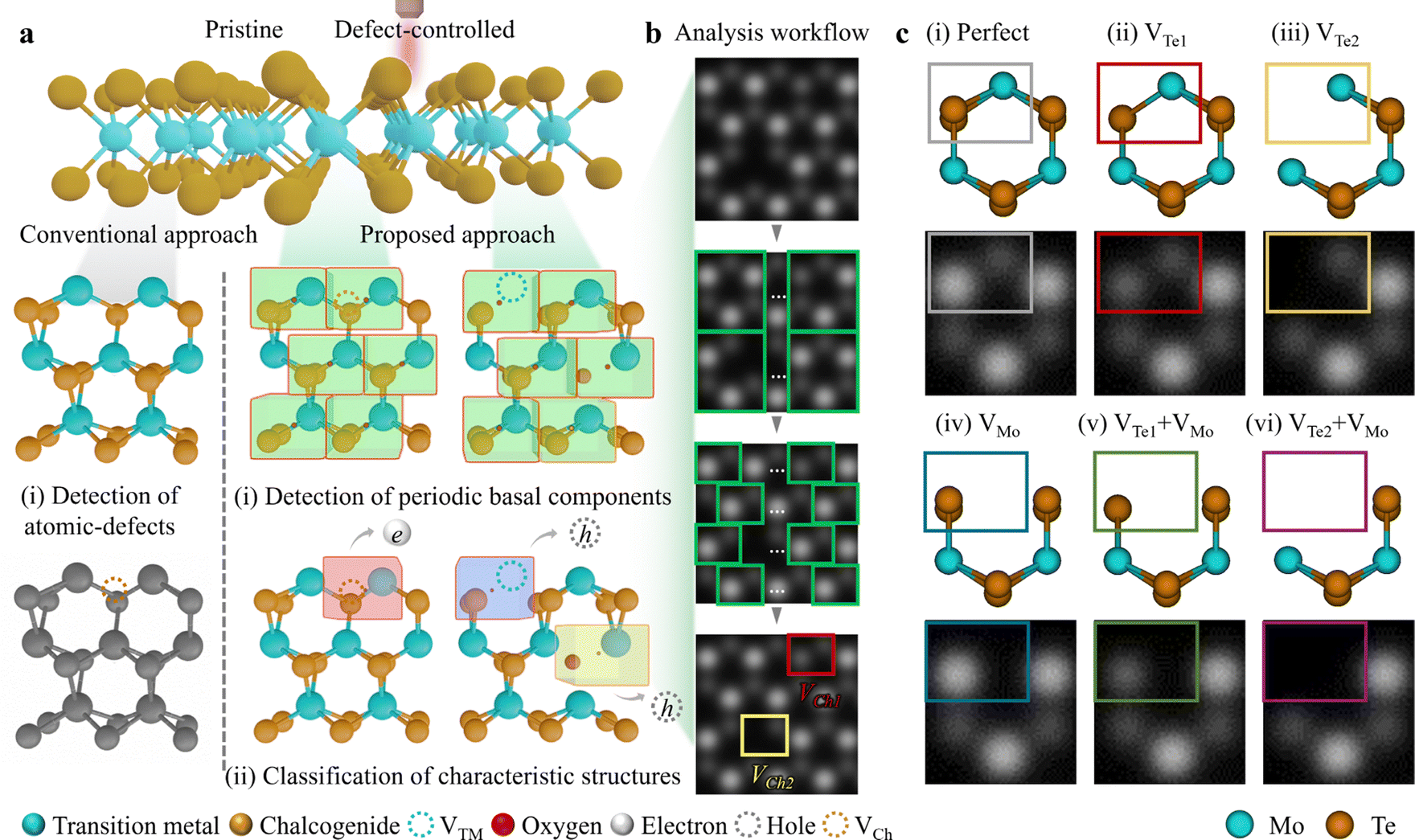 | ||
| Fig. 1 Synergy of object (unit cell) detection and (point defect) classification expressing workflow to analyse point defects. (a) (Top) Schematic of pristine and defect-controlled TMDCs. (Left-middle)-(Left-bottom) Conventional point defect identification of chalcogenide (Ch) or transition metal (TM) sites. (Centre-middle)-(Right-middle) Detections of unit cells (green boxes) of pristine and defect-controlled TMDCs. Since the periodic-basal components are unit cells, the detection of every unit cell is a prerequisite as the enumeration manner. (Centre-bottom)-(Right-bottom) Classifications of distinctive defects in unit cell-level (colour-coded boxes) as denoted by the “Proposed approach”. The identification of characteristic defects is essential to correlate (i) defect structures and (ii) their physical impacts on TMDCs. The red box incorporated with chalcogenide vacancy (VCh) exhibits an n-type characteristic by electrons, while the blue (yellow) box with a transition metal vacancy (VTM) (oxygen chemisorption at VCh) exhibits a p-type characteristic by holes. (b) Workflow to examine point defects. From the input, green hexagonal cells are detected; then further unit cell (green) cropping is conducted. Eventually, the point defect types are classified at the unit cell level: chalcogen monovacancy (VCh1, red rectangle) or chalcogen divacancies (VCh2, yellow rectangle). (c) (Top) Atomic models with (i) Perfect (grey), (ii) VTe1 (red), (iii) VTe2 (yellow), (iv) VMo (blue), (v) VTe1 + VMo (olive), and (vi) VTe2 + VMo (purple) for ML 2H-MoTe2 in each unit cell. (Bottom) Simulated HAADF-STEM images corresponding to the top panels. The colour-coded rectangles are adopted as the simulation data set for the “Proposed approach”. | ||
Fig. 1c illustrates representative point defects in ML 2H-MoTe2; (i) Perfect (non-defective, grey), (ii) VTe1 (Te monovacancy, red), (iii) VTe2 (Te divacancies, yellow), (iv) VMo (Mo monovacancy, blue), (v) VTe1 + VMo (Te monovacancy with Mo monovacancy, olive), and (vi) VTe2 + VMo (Te divacancies with Mo monovacancy, purple) in colour-coded rectangles. Conventionally, defect types e.g. Perfect, VTe2, and VTe1 are defined by matching simulation and experimental HAADF-STEM images through intensity profiling (see Fig. S1 and supplementary text 1 for details in the ESI†). This manual intensity profiling to define point defects inspires the defect examination process by deep learning with the construction of a simulation dataset. Furthermore, the basal repetition components in materials are unit cells, and we focused on the different contrasts in each unit cell shown in the colour-coded rectangles in the top and bottom panels of Fig. 1c. Obviously, we designed a CNN-based analytic platform (2DIP-Net) by utilising these various simulation datasets.
Here, we generated a simulation dataset using “Dr Probe”, which is widely used for STEM image simulation, mirroring the atomic-structural imaging conditions: (i) camera length of 6 cm (HAADF imaging condition); inner-outer angle of 70.0–277.9 mrad, (ii) condenser aperture radius of 27 mrad. For the CNN-1, Poisson/Gaussian noise was added to a total of 500 training data and 50 validation data. For the simulation data set of the CNN-2, Poisson/Gaussian noise was added using one each of the six types of simulation data set. By adding noise, a total of 4800 training data (800 data for each defect type) and 1200 validation data (200 data for each defect type) were created (see more details in Fig. S2 to generate the simulation dataset and supplementary text 2 in the ESI†).
It is prerequisite to detect the accurate unit cell location as the first-phase of point defect analysis. However, for a defect type with weak contrast, such as VTe2 + VMo, the position (boundary) of the unit cell is ambiguous. Therefore, we trained the CNN-1 to detect hexagonal cells from an input followed by a post-process to extract the unit cell from the hexagonal cell. We nominated these two procedures as a “hexagonal net-casting process”. This approach is expected to tightly crop the unit cell, even with weak contrast e.g. VTe1 + VMo or VTe2 + VMo in a material.
Fig. 2a describes the CNN-1 architecture illustrating analysis workflow. By combining the simulation dataset in Fig. 1c to create a CNN-1 input, a series of convolution i.e. “Conv Block”-“Inverted Residual block”-“Feature map” is through by MobileNet V2. Then, with the combination of the (i) Region Proposal Network and (ii) Fast RCNN, the final location of hexagonal cells is predicted. Here, the CNN-1 is trained to accurately predict the size and location of hexagonal cells (referred to as “Predicted bbox” in “CNN-1 Output”), compared to the ground truth of the hexagonal cell (red) (see more details in Fig. S3a and S4a and supplementary text 3 in the ESI† for the training process and the training/validation loss curves of CNN-1). To eventually crop the unit cell from the hexagonal cell, the crop-ratio is defined of (i) α = WU/WH (width of unit cell/width of hexagonal cell) and (ii) β = HU/HH (height of unit cell/height of hexagonal cell). Then, the coordinates of “A”, “B”, “C”, and “D” are defined as follows: A (xmin, ymin); B (xmin + α × WH, ymin + β × HH); C (xmax − α × WH, ymax − β × HH); D (xmax, ymax). These coordinates are utilised to extract two green unit cells, which are post-processed from one green hexagonal cell in Fig. 2b.
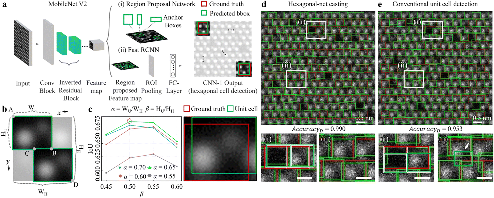 | ||
| Fig. 2 Unit cell detection performance evaluation by CNN-1. (a) The architecture of CNN-1 to detect the hexagonal cell from the input. The MobileNet V2 convolute the input through “Conv block”-“Inverted Residual block”-“Feature map”. The (i) region proposal network and (ii) fast RCNN finally predict the size and location of the hexagonal cell (as indicated by the green “Predicted bbox” in the “CNN-1 Output”) compared to the red “Ground truth”. (b) Enlarged hexagonal cell and post-process to crop the unit cell. The coordinates of “A”, “B”, “C”, and “D” are extracted as follows; A (xmin, ymin), B (xmin + α × WH, ymin + β × HH), C (xmax – α × WH, ymax − β × HH), and D (xmax, ymax). Here, for the post-process, crop-ratios are defined by two parameters: (i) α = WU/WH (width of unit cell/width of hexagonal cell) and (ii) β = HU/HH (height of unit cell/height of hexagonal cell). (c) (Left) Estimation of Intersection over Union (IoU), accordingly with α from 0.55 to 0.70 (0.05 increment) and β from 0.45 to 0.60 (0.05 increment). (Right) Definition of IoU: “Intersection of ground truth (green box) and final unit cell (red box)” divided by “Union of ground truth and final unit cell”. Through all crop-ratio values, α (β) of 0.65 (0.5) exhibited the most IoU of 0.691. (d) and (e) (Top) The competence of the “hexagonal-net casting process” and conventional unit cell detection process, respectively. The green (red) boxes indicate the size and location of predicted unit cell (ground truth). (Bottom-left) ((Bottom-right)) Enlarged unit cell detection results of (i) ((ii)) in the white boxes in (e) ((f)). Scale bars; 0.2 nm. The averaged unit cell detection accuracies are 0.990 (0.953) for hexagonal-net casting (conventional unit cell detection), calculated with the ratio of the “number of unit cells with an IoU greater than 0.5” to the “total number of examined unit cells (1691)”. | ||
To assess the performance of the hexagonal-net casting process, we estimated the Intersection over Union (IoU). The left panel in Fig. 2c calculates the IoUs obtained by varying α from 0.55 to 0.70 (0.05 increment) and β from 0.45 to 0.60 (0.05 increment). Through the entire examinations, α (β) of 0.65 (0.5) displayed the highest IoU of 0.691 (red dotted circle) i.e. high accuracies for unit cell detection). Here, the IoU is defined by “Intersection area of ground truth (red) and detected unit cell (green)” divided by “area of ground truth and detected unit cell” (right panel in Fig. 2c). For our evaluation, we tested simulation HAADF-STEM images since the unit cell boundary in experimental images is uncertain.
We further compared our (i) hexagonal-net casting process (Fig. 2d) and (ii) conventional unit cell detection (Fig. 2e, here, CNN-1 is trained to directly detect unit cells). The top panels in Fig. 2d and e are unit cell detection results in noised-simulation HAADF-STEM images. In a wide field-of-view, it seems that both processes are not very different. However, in enlarged micrographs (left-bottom and right-bottom panels), the conventional approach shows (i) either deviated unit cell detection compared to ground truth (white rectangles (i) in Fig. 2d and e) and more critically, (ii) mis-detected unit cell (false positive, white rectangles (ii) in Fig. 2d and e as indicated by the white arrow). The overall unit cell cropping accuracies of the hexagonal-net casting process (conventional approach) for 0.990 (0.953). The accuracies were estimated by calculating the ratio of “number of unit cells with an IoU greater than 0.5” to the “total number of examined unit cells (1691)”. Through Fig. 2, by varying the crop-ratio of α (β) to extract the unit cell from the hexagonal cell, we found that an α (β) of 0.65 (0.5) was optimal for the post-process step.
During STEM imaging, contamination (or polymer residue) on a sample falsifies the image contrast/brightness in either the Mo- or Te2-column site. Additionally, the two atomic columns in each unit cell do not all have the same tendency of contrast/brightness variations during experiment. Inspired by point defect determination with manual intensity profiling (Fig. S1, ESI†), we estimated the point defect classification competence of CNN-2 using two-types of input. These types include (i) 1-channel (1 ch-) input; the whole unit cell and (ii) 2-channel (2 ch-) input; separated Mo/Te2-column parts from the unit cell, and then paired together (Fig. 3a). We anticipate that point defect classification comparison of CNN-2 between 1 ch- and 2 ch-input types will provide new insight to improve the accuracies of point defect analysis through deep learning.
 | ||
| Fig. 3 Point defect classification performance evaluation by CNN-2. (a) The architecture of CNN-2 to classify point defects from 1 ch- (a whole unit cell) and 2 ch-inputs (atomic-column separated). By ResNet-18, the inputs are through “Conv Block”-“Residual block”-“Feature map”-“Global average pooling”-“FC-layer” to classify point defect types as one of the simulated dataset in each unit cell. (b) and (c) Point defect classification results with experimental images with 1 ch- and 2 ch-input of CNN-2 from the identical CNN-1 output. The grey (red) arrows in (b) are misclassified to Perfect (VTe1); ground truth of VTe1 (VTe2). Likewise, the red arrow in (c) is misclassified to VTe1; ground truth of Perfect. The colour-codes are the same as in Fig. 1. (d) Corresponding ground truth of (b) and (c). Scale bars, 0.5 nm. (e) Accuracies for point defect classification performance of total 11 input experimental images (3037 unit cells examined) of 1 ch-input (light blue) and 2 ch-input (light pink), respectively. The accuracies for Perfect, VTe1, VTe2 and VMo for 1ch-(2ch-) input are 100% (100%), 52.48% (97.87%), 35.71% (100%), and 33.33% (100%), respectively. | ||
Fig. 3a describes the CNN-2 architecture illustrating the analysis workflow. From two-types of input (1 ch- or 2 ch-input), a series of processes i.e. “Conv Block”-“Residual block”-“Feature map”-“Global average pooling”-“FC-layer” is through by ResNet-18. Subsequently, each point defect species is predicted as one of the six simulation datasets (see more details in Fig. S3b and S4b and supplementary text 3 in the ESI† for the training processes and the training/validation loss curves of CNN-2). We examined point defects in experimental HAADF-STEM images of ML 2H-MoTe2; Fig. 3b(c) for 1 ch- (2 ch-) input-type and Fig. 3d for ground truth, from the identical CNN-1 output (see more details to examine point defect for simulation images in Fig. S5–S9 and Supplementary text 4 in the ESI†). The grey (red) arrows in Fig. 3b are mis-classified to Perfect (VTe1); ground truth of VTe1 (VTe2). Likewise, the red arrow in Fig. 3c is mis-classified to VTe1; ground truth of Perfect. Although not explicitly indicated for clarity, Perfect unit cells were also classified. The analytical accuracies of (i) Perfect, (ii) VTe1, (iii) VTe2, and (iv) VMo of 1 ch-input for light blue (2ch-input for light pink) were (i) 100% (100%), (ii) 52.48% (97.87%), (iii) 35.71% (100%), and (iv) 33.33% (100%) (more analytic results are presented in Fig. S10–S13 to examine point defects in experimental images, ESI†).
In particular, the accuracy of point defect classification for 2 ch-input significantly improved compared to 1 ch-input (Fig. 3e). These results suggest that the 2 ch-input type is optimal to examine point defects in experimental images. Given the limited image features of atomic position and brightness, it can be challenging to classify six different point defect species (including the Perfect type). We believe this approach provides more clues to CNN-2 to classify different point defects species to determine (i) “Te-on site” defects primarily i.e. VTe1, VTe2, or non-defective, and (ii) “Mo-on site defects” secondarily i.e. VMo or non-defective. With the combination of the Te-on site and Mo-on site defect determination, CNN-2 could decide the eventual defect types.
So far, we designed a dual-mode CNN-platform i.e. 2DIP-Net to examine point defects in 2H-MoTe2 (Fig. 4a). Through Fig. 2 and 3, we inspected the (i) unit cell detection and (ii) point defect classification with the simulation dataset. The CNN-1 (CNN-2) performed elaborate unit cell detection (accurate point defect classification). Still, there is an urge for systematic noise-added exploration to simulation dataset to ensure reliable point defect analysis in experimental images. Noise is the main simulation dataset construction factor in our study since it is the primary bottle-neck and challenge to identify accurate point defects. However, a quantitative noise estimation in the electron microscopic image has not been developed.47,49,50 Therefore, we estimated the point defect analysis accuracies of 2DIP-Net, by varying Poisson or Gaussian noise during simulation dataset construction. We anticipated that we could propose the appropriate amount of noise to analyse point defects in experimental images with a simulation dataset.
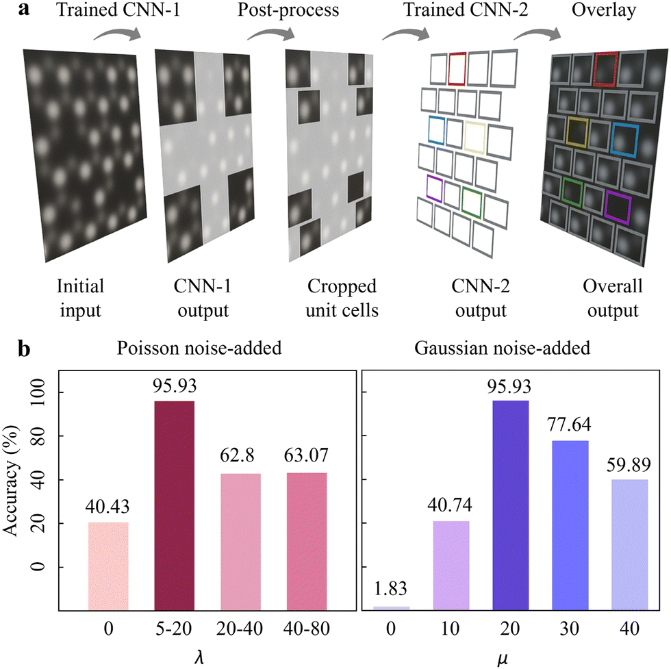 | ||
| Fig. 4 (a) Overall point defect classification procedure of 2DIP-Net. (b) (Left)((Right)) Overall point defect classification accuracies for experimental images by varying λ (μ) values to the simulation dataset. The λ is ranged: (i) λ = 0 (non-Poisson), (ii) 5 ≤ λ ≤ 20, (iii) 20 ≤ λ ≤ 40, and (iv) 40 ≤ λ ≤ 80; while μ is fixed: (i) μ = 0 (non-Gaussian), (ii) μ = 10, (iii) μ = 20, (iv) μ = 30, and (v) μ = 40. Here, 5 ≤ λ ≤ 20 (μ = 20) was the most efficient for point defect classification accuracies up to 95.93% (95.93%). Note that classification accuracy for Perfect types are not considered to only suggest for the defects. | ||
Since Poisson is the dominant noise type during STEM imaging,58,59 we ranged the Poisson noise parameter λ to cover various experimental STEM images: (i) λ = 0 (non-Poisson), (ii) 5 ≤ λ ≤ 20, (iii) 20 ≤ λ ≤ 40, and (iv) 40 ≤ λ ≤ 80, while the Gaussian noise parameter μ was fixed: (i) μ = 0 (non-Gaussian), (ii) μ = 10, (iii) μ = 20, (iv) μ = 20, and (v) μ = 40. The histograms in Fig. 4b show the overall point defect classification accuracies for “experimental” HAADF-STEM images, corresponding to the Poisson noise-added (left) and Gaussian noise-added (right) dataset, respectively. Based on our examination, 5 ≤ λ ≤ 20 (μ = 20) was the most efficient towards point defect analysis reaching 95.93% (95.93%) accuracy (see more details in Fig. S14 and supplementary text 5 in the ESI† for training results of 5 ≤ λ ≤ 20 and μ = 20).
We proceeded to compare point defect classification competence between 2DIP-Net (with 2 ch-input type) and the FCN-based approaches as reported in previous studies47–50 (see more details about FCN in Fig. S15 and supplementary text 6 in the ESI†). Fig. 5a illustrates the 2DIP-Net (top) and FCN-based (bottom) point defect classification results for experimental images. Here, the Perfect types were classified though they are not indicated for clarity. In the enlarged HAADF-STEM images of Fig. 5b and c top (2DIP-Net) and bottom (FCN) panels from the colour-coded rectangles in Fig. 5a, it becomes evident that the FCN model is often confused about distinguishing between VTe1 (green) or VTe2 (dark-red), as indicated by red arrows. The 2DIP-Net identified the point defect type in the unit cell accommodating VTe1. In the same region, though, the FCN predicted the point defect species of VTe1 (green) vs. VTe2 (red) at the pixel level within one VTe1 site. In this case, human intervention may be necessary to determine the defect types between VTe1 and VTe2. Based on Fig. 5d, these confusions of FCN were confirmed by estimating the proportion of confidence (POC) of VTe1vs. VTe2; 40.6% vs. 59.4% and 59.6% vs. 40.4%. In contrast, 2DIP-Net exhibited much higher POCs for VTe1vs. VTe2; 89.6% vs. 10.4% and 87.2% vs. 12.8%. Furthermore, we stretched out to examine the classification competence between Perfect and Te-on site defects; VTe1 and VTe2 for simplicity, as presented in the top (2DIP-Net with 2 ch-input) and bottom panels (FCN) in Fig. 5e. From a total of 3034 unit cells examined, the FCN was confused when determining the defect type of VTe1vs. Perfect: 6 mis-classified to Perfect while ground truth of VTe1 (up to 95.7% accuracy). In contrast, our 2DIP-Net is more accurate; 3 mis-classified to Perfect with a ground truth of VTe1 (up to 97.9% accuracy).
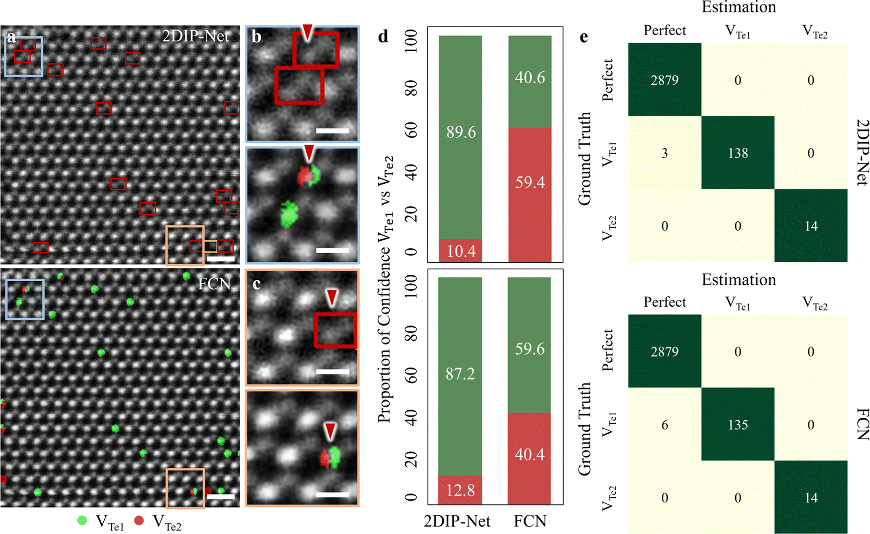 | ||
| Fig. 5 (a) (Top)-(Bottom) Point defect classification results by 2DIP-Net (with 2 ch-input) and FCN, respectively. Scale bars: 0.5 nm. (b) and (c) (Top)-(Bottom) Enlarged HAADF-STEM micrographs as marked light blue and light orange in (a) and (b), respectively. Scale bars: 0.2 nm. (d) (Top)-(Bottom) Proportions of confidence (POC) of VTe1 (green) vs. VTe2 (dark-red) as denoted by red arrows in the top panels in (b) and (c), respectively. The 2DIP-Net exhibited much higher POCs than FCN for VTe1vs. VTe2; 89.6% vs. 10.4% and 87.2% vs. 12.8% by 2DIP-Net and 40.6% vs. 59.4% and 59.6% vs. 40.4% by FCN. (e) (Top)-(Bottom) Confusion matrices for Perfect and Te-on site defects of 11 total input experimental images (3034 unit cells examined) by 2DIP-Net and FCN, respectively. The 2DIP-Net (FCN) performed 97.9% (95.7%) classification accuracies for VTe1. | ||
To advance our approach and create a comprehensive database for diverse point defect classification, we developed a Graphic User Interface (GUI)-based point defect examination tool (Fig. 6a). By loading an input STEM image, the results are presented of classified point defect types. Here, Perfect (grey) and other colour-coded defect types are identified, and the results can be cross-validated by profiling atomic-intensities. Neither limited to mechanically exfoliated 2D materials nor other species of materials, our approach can cover various types of defect-susceptible and atomic contrast sensitive materials exhibiting fascinating physical properties. Using this GUI, we statistically defined point defect species in pristine 2H-MoTe2 experimental images. After examining a total of 3037 unit cells (including Perfect types), it was confirmed the extant point defect species are (i) VTe1 (red), (ii) VTe2 (yellow), and (iii) VMo (blue), respectively (left and middle panels in Fig. 6b). Enlarged hexagonal cells (right panels in Fig. 6b) labelled (i), (ii), and (iii) representatively visualise the enlarged hexagonal cells. In Fig. 6c left panel, we specified the defect-concentrations in pristine 2H-MoTe2: the concentration of VTe1 (red) was 7.16 × 1020 cm−2, followed by VTe2 (yellow) of 4.38 × 1019 cm−2 and VMo (blue) of 1.4 × 1019 cm−2 (total analysed area of 2.053 × 1019 cm2 (205.3 nm2). Note that the VTe1 + VMo or VTe2 + VMo (referred to as multiple defect types) confirmed undetected in our estimation (see more details in Fig. S13, ESI†). These multiple defect types are less likely to transpire by minimal external stimuli.59 However, the extant point defects may be generated during transmission electron microscopy (TEM) sample preparation by mechanical exfoliation.59,60
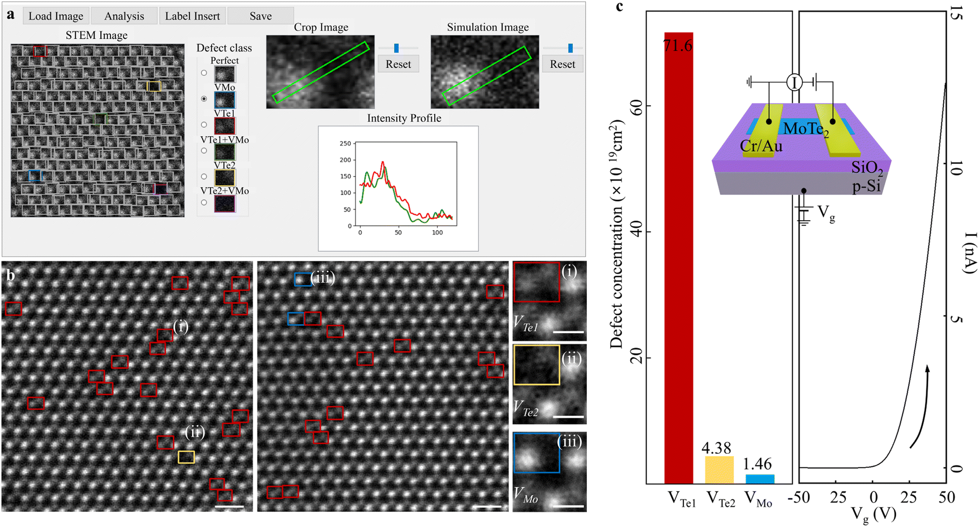 | ||
| Fig. 6 (a) GUI-based point defect analysis expendable to accumulate training data base. From the input, the classified point defect types are visualised as one of the simulation datasets in the unit cell-by-unit cell (in the “STEM image” panel). We can select each defect-classified unit cell in the “Crop Image” panel and compare the intensity in the “Simulation Image” panel by choosing one of the simulation datasets from the “Defect class” panel. (b) (Left)-(Middle) Point defect classification results by 2DIP-Net (by GUI) in the experimental images. Totally, the classified point defects are categorised into three types: VTe1 (red), VTe2 (yellow), and VMo (blue). Scale bars: 0.5 nm. (Right) Enlarged point defect identifications in rectangles (i)-(iii) in the left and middle panels of VTe1, VTe2 and VMo, respectively. Scale bars: 0.2 nm. (c) (Left) The defect-concentrations of (i) 7.16 × 1020 cm2 (VTe1), (ii) 4.38 × 1019 cm2 (VTe2), and (iii) 1.46 × 1019 cm2 (VMo). The total analysed area of 2.053 × 1019 cm2 (205.3 nm2) corresponding to a total of 3037-examined unit cells. The colour-codes are the same as in Fig. 1. Scale bars: 0.5 nm. (Right) Transfer (I–Vg) curve of 2H-MoTe2 back-gated FET. The transfer result reveals that the pristine 2H-MoTe2 exhibits n-type characteristics. Inset: Schematic of back-gated FET for transfer measurement. | ||
To further correlate defect-electrical properties, we fabricated a back-gated field effect transistor (FET), with the identical exfoliation method as in TEM sample preparation. As illustrated in Fig. 6c right panel, we verified that the n-type character dominantly originated from Te-vacancies. Here, our full-automated and statistical approaches to analyse point defects could contribute to minimize the gap that should be correlated by (i) preparing a TEM sample and (ii) fabricating a device to correlate (i) an atomic defect structure-(ii) electric property unit.
Discussions
To achieve atomic-structural analysis in automated and statical fashions, unit cell detection is the first-phase, as mentioned in Fig. 2. In the HAADF-STEM image at a magnification of 20 million (20 M), the size of (i) the unit cell and (ii) the hexagonal cell for 2H-MoTe2 is about (i) 75 pixels (WU) × 65 pixels (HU) and (ii) 120 pixels (WH) × 130 pixels (HH), respectively. At magnifications lower than 20 M, cropping unit cells becomes more challenging due to degraded image resolutions. Our hexagonal-net casting can set boundaries in atomic-structural images even for multiple defect types and this efficiency was demonstrated by deciding unit cell crop-ratio α (WU/WH) and β (HU/HH). We found that α = 0.65 (β = 0.5) exhibited the highest efficiency with an IOU of 0.691. Furthermore, due to the limited image features of the unit cell; only two atomic-columns with different contrast (brightness), the CNN-1 may insufficiently learn image features to accurately crop unit cells. By training CNN-1 to recognise “hexagonal cells”, (i) six atomic columns with (ii) different contrast (brightness) and (iii) hexagonal atomic-arrangement of Mo- and Te2-columns could provide additional image features to increase the possibility of unit cell detection.From a material-perspective, usually, the unit cell of 2D materials is a parallelogram; lattice parameter of a = b ≠ c, and angles of α = β = 90°, γ = 120°. However, from an image process-perspective, it is difficult to deal with a parallelogram unit cell, since the rectangular region of interest (ROI) is common. Therefore, the hexagonal-net casting process can interconnect the materials (analysis) and image-process through a deep learning technique. This can be achieved by substituting the analysis dimension with parallelograms (for materials) and rectangles (for image-process). We also discovered that the α = 0.65 (β = 0.5) coincide with experimental HAADF-STEM images at a magnification of 20 M: WU/WH (HU/HH) of 0.63 (0.5). We systematically explored the unit cell cropping performance of CNN-1, to our best knowledge, which hereto unaddressed subjects.
We examined point defect classification competence by comparing a 1 ch-input and 2 ch-input in Fig. 3. The confusion of Perfect vs. VTe1 was revealed in a 1 ch-input type, since not all the two atomic columns have the same tendency of contrast/brightness variations during STEM experiment. With the limited image features-atomic position and brightness, it can be challenging to classify six different point defect species (including the Perfect type). We believe that separating the atomic columns (2 ch-input) provides additional clues to CNN-2, enhancing the accuracy of point defect classification. These additional image features aid the CNN-2 in primarily determining “Te-on site” defects, i.e., VTe1, VTe2, or non-defective, and secondarily determining “Mo-on site defects,” i.e., VMo or non-defective.
The noise-added values of λs and μs to the simulation dataset achieved minimal loss during training (Fig. S14, ESI†). However, in Fig. 4b, the accuracies of point defect classification in experimental images showed significant deviations: (i) 95.93% (5 ≤ λ ≤ 20) followed by 63.07% (40 ≤ λ ≤ 80), 62.8% (20 ≤ λ ≤ 40) and (ii) 40.43% (non-Poisson), and 95.93% (μ = 20), 77.64% (μ = 30), 59.87% (μ = 40), 40.74% (μ = 10) and 1.83% (non-Gaussian). These results give us the two instructions for deep learning-based point defect analysis. Frist, point defect classification should be cross-validated by examining experimental images, though the training process seemingly goes well. Second, these explorations provide us with insights into the optimal degree-of-noise levels utilising simulation datasets towards point defect identification in experimental STEM images. Note that we trained both CNN-1 and CNN-2 using the optimal noise values as revealed in Fig. 4.
As depicted in Fig. 6, the identification of point defects in pristine 2H-MoTe2 is an essential study to further explore defect-engineered 2H-MoTe2. Previous study revealed a point defect concentration of pristine 2H-MoTe2 of 5.8 × 10¹¹ nm2;61 however, this report neither differentiated Te-on site nor Mo-on site defects. The properties of crystal systems, in relation to the contribution of defect species, have not been thoroughly explored, necessitating further investigation. In our study, we identified three types of point defects in pristine 2H-MoTe2. While VMo acts as a p-type dopant to the 2H-MoTe2 crystal,35 the large concentration of the n-type characteristics of VTe1 and VTe2 counteracted the p-type behaviour of VMo. Furthermore, the use of mild STEM imaging conditions made it possible to apply deep learning techniques to atomic-structural images with minimal significant degradations (see more details in the methods section).
Still, there remain issues to be resolved for accurate point defect inspection using deep learning. Frist, we trained 2DIP-Net using a simulation dataset towards experimental image analysis. Though we applied (added) Poisson (Gaussian) noise to the simulation dataset with optimal degree-of-noise values to mirror experimental HAADF-STEM imaging conditions, a quantitative noise estimation method in the field of electron microscopy has not yet been developed.47,49,50 If such a quantifiable noise approximation technique is established, a more dependable point defect investigation can be realised. Second, we should consider the fact that, in actual HAADF-STEM images, there is a lack of ground truth for point defects as the training database.47 This issue also applies to other deep learning-based point defects studies in atomic-resolution images. Our approach may contribute to solving this issue by accumulating a database for a defined point defect in experimental images. More authentic analysis may be guaranteed for future point defect analysis based on deep learning, and our developed GUI could relieve the difficulties in building a training database (Fig. 6a).
Conclusions
In this work, we established a deep learning-based platform i.e. 2DIP-Net to investigate a variety of point defects and their influence on the electrical properties of pristine 2H-MoTe2via atomic-structural imaging. To address the limitations of the training data e.g., the lack of ground truth for point defect, we intensively constructed a simulation dataset to reflect the experimental conditions by adding noise. To enhance the accuracy of (i) unit cell detection and (ii) point defect classification, we (i) segmented detected hexagonal cell into unit cells and then (ii) separated the 1 ch-input into 2 ch-input. With the limited image features in HAADF-STEM images, the partitioning of the analysis process or target elements in each step can lead to more accurate results, which have not been addressed previously. We believe our approach efficiently analyses simple-featured images by appropriately delimitating periodic boundaries within the images. With this approach, we unveiled that point defects in pristine ML 2H-MoTe2 were classified with concentrations of (i) VTe1, (ii) VTe2, and (iii) VMo was (i) 7.16 × 1020 cm2, (ii) 4.38 × 1019 cm2, and (iii) 1.46 × 1019 cm2. Our atomistic defect study of pristine 2H-MoTe2 can suggest the avenue to systematically inspect defect-modulated 2H-MoTe2, which was explicated neither by theoretical approaches nor experimentally in statistical manners.36,38,60,62Methods
TEM sample preparation and STEM imaging
To acquire highly crystalline pristine 2H-MoTe2, we mechanically exfoliated ML 2H-MoTe2 from bulk 2H-MoTe2 as reported in previous work.63 To minimise the electron beam-induced point defects in 2H-MoTe2, we used mild STEM imaging conditions with an acceleration voltage of 80 kV. To compensate for the debased resolution due to the low acceleration voltage, we employed 5th-order aberration-corrected (Cs-corrected) STEM (JEOL JEM-ARM200F), at the Materials Imaging & Analysis Center of POSTECH in South Korea. We acquired atomic-resolution HAADF-STEM images using Z-contrast to analyse the point defect concentrations. Recently pre- and post-image processing techniques of STEM imaging with a high signal-to-noise ratio and a few picometer resolution have been achieved via noise filtering,39 rigid registration,40 and non-rigid registration.41 However, these processes manage an image intensity issue which is a crucial factor for Z-contrast imaging in HAADF-STEM, and they may leave room for Z-contrast distortion in an image. Therefore, we acquired a single scanned image (2048 pixels × 2048 pixels) over a short dwell time of 5–6 μs per pixel, also relieving sample linear drift-related image distortion.STEM image simulation to construct a dataset
To mimic the experimental conditions of our experimental set-up, we generate a simulation dataset as follows: (i) acceleration voltage of 80 kV, (ii) camera length of 6 cm; inner-outer angle of 70.0–277.9 mrad, (iii) condenser apertures radius of 27 mrad, and (iv) probe size of 0.6 Å. Note that an experimental point defect STEM image training database for 2D materials does not exist;47 therefore, we emulated experimental images using simulated images. For CNN-1 and CNN-2, the main simulation image construction factor is a Poisson (Gaussian) noise parameter of 5 ≤ λ ≤ 20 (μ = 20) to each simulated image.Elaborate unit cell extraction
For accurate point defect classification, precise detection of unit cells should be performed. Therefore, the role of CNN-1 is crucial in the first-phase of the point defect analysis. Fig. 2b illustrates our hexagonal-net casting process; once a hexagonal cell is recognised by CNN-1, the coordinates of “A”, “B”, “C”, and “D” are determined for further cropping of the unit cells. The width and height of the hexagonal cell is the difference between the maximum and minimum x coordinate (xmax− xmin) and the difference between the maximum and minimum y coordinate (ymax− ymin), respectively. Subsequently, the left upper and right lower unit cells in the hexagonal cell were further cropped. This cropping technique increased the capability of detecting unit cells precisely.Appropriate input types for point defect classification
Providing the appropriate input for the CNN-2 model to discriminate different types of point defects was key for accurate defect classification. Fig. 3a illustrates two types of input types fed into CNN-2. As the contrast comparison between the Te2 and Mo column is used to classify point defects, we proposed a 2 ch-input, dividing the Te2 column and Mo column parts by half along the x-axis of the unit cell. Then, the two separated images were resized and stacked to form a 2 ch-input.Deep learning architectures for the optimized analytic phase
CNN-1 was composed of a pre-trained mobilenet-v2 feature extractor and the region proposal network.64 The anchor box size of the region proposal network was (8, 16, 32, 64, 128), and the ratio used to create various bounding box candidates was (0.5, 1.0, 2.0). In addition, for one input image, the maximum number of detection boxes was set to 800. The CNN-1 was trained for 40 epochs using the Adam optimizer (learning rate: 1 × 10⁻⁴) by smooth L1 loss and cross-entropy loss. The CNN-2 was composed of the Resnet-18 feature extractor and a fully connected (FC) layer. A total of 512 nodes were created through the global average pooling layer. The last feature extractor and a 512 × N (N = number of layer classes) FC layer were constructed. We trained the CNN-2 using the cross-entropy loss function for 40 epochs with the same optimizer (learning rate: 2 × 10⁻⁶) as CNN-1. The input size for CNN-1 was resized to 512 × 512, and the output of CNN-1 was the bounding boxes (xmin, ymin, xmax, ymax) of hexagonal cells. Subsequently, through post-processing, two unit cells were cropped from the hexagonal cells. For the CNN-2, one half of the unit cell image was divided as a 2 ch image using the vertical axis of the unit cell image as a perforated line. After resizing to 224 × 224, the images were fed to CNN-2 for point defect classification. The CNN architectures for the end-to-end analysis method in this study were designed using PyTorch, which is a Python-based framework and trained with a 11 GB NVIDIA RTX 2080Ti graphics card.Dataset availability
The codes and dataset used in this study are available from the corresponding author upon reasonable request. Also, our GUI is publicly available on GitHub (https://github.com/wormschu/Point-defect-analysis-GUI)Author contributions
D.-H. Y., and Y.-S. C. contributed equally to this work and were supervised by S. Y. and S.-Y. C.Conflicts of interest
There are no conflicts to declare.Acknowledgements
S.-Y. C. acknowledges the support of the Korea Basic Science Institute (National research Facilities and Equipment Center) grant funded by the Ministry of Education (2020R1A6C101A202) and the Institute for Basic Science (IBS-R034-D1). S. Y. acknowledges the support of a National Research Foundation of Korea grant provided by the Korean government (Ministry of Science and ICT) (NRF-2022R1A2C2091160).References
- S. M. Hus and A. P. Li, Prog. Surf. Sci., 2017, 92(3), 176–201 CrossRef CAS.
- K. S. Novoselov, A. Mishchenko, A. Carvalho and A. H. C. Neto, Science, 2016, 353(6289), aac9439 CrossRef CAS PubMed.
- O. V. Yazyev and Y. P. Chen, Nat. Nanotechnol., 2014, 9, 755–767 CrossRef CAS.
- Z. Lin, B. R. Carvalho, E. Kahn, R. Lv, R. Rao, H. Terrones, M. A. Pimenta and M. Terrones, 2D Mater., 2016, 3, 022002 CrossRef.
- H. Qiu, T. Xu, Z. Wang, W. Ren, H. Nan, Z. Ni, Q. Chen, S. Yuan, F. Miao, F. Song, G. Long, Y. Shi, L. Sun, J. Wang and X. Wang, Nat. Commun., 2013, 4, 2642 CrossRef PubMed.
- M. M. Ugeda, D. Fernández-Torre, I. Brihuega, P. Pou, A. J. Martínez-Galera, R. Pérez and J. M. Gómez-Rodríguez, Phys. Rev. Lett., 2011, 107, 116803 CrossRef CAS.
- D. Jariwala, V. K. Sangwan, L. J. Lauhon, T. J. Marks and M. C. Hersam, ACS Nano, 2014, 8(2), 1102–1120 CrossRef CAS PubMed.
- Y. Gong, J. Lin, X. Wang, G. Shi, S. Lei, Z. Lin, X. Zou, G. Ye, R. Vajtai, B. I. Yakobson, H. Terrones, M. Terrones, B. K. Tay, J. Lou, S. T. Pantelides, Z. Liu, W. Zhou and P. M. Ajayan, Nat. Mater., 2014, 13, 1135–1142 CrossRef CAS PubMed.
- S. McDonnell, R. Addou, C. Buie, R. M. Wallace and C. L. Hinkle, ACS Nano, 2014, 8, 2880–2888 CrossRef CAS PubMed.
- D. Wu, X. Li, L. Luan, X. Wu, W. Li, M. N. Yogeesh, R. Ghosh, Z. Chu, D. Akinwande, Q. Niu and K. Lai, Proc. Natl. Acad. Sci. U. S. A., 2016, 113, 8583–8588 CrossRef CAS.
- K. Dolui, I. Rungger, C. D. Pemmaraju and S. Sanvito, Phys. Rev. B: Condens. Matter Mater. Phys., 2013, 88, 075420 CrossRef.
- J. Suh, T.-E. Park, D.-Y. Lin, D. Fu, J. Park, H. J. Jung, Y. Chen, C. Ko, C. Jang, Y. Sun, R. Sinclair, J. Chang, S. Tongay and J. Wu, Nano Lett., 2014, 14(12), 6976–6982 CrossRef CAS PubMed.
- Y. Jin, D. H. Keum, S.-J. Kim, H. S. Lee and Y. H. Lee, Adv. Mater., 2015, 27, 5534–5540 CrossRef CAS PubMed.
- L. Yang, K. Majumdar, H. Liu, Y. Du, H. Wu, M. Hatzistergos, P. Y. Hung, R. Tieckelmann, W. Tsai, C. Hobbs and P. D. Ye, Nano Lett., 2014, 14, 6275–6280 CrossRef CAS.
- Y. Chen, J. Xi, D. O. Dumcenco, Z. Liu, K. Suenaga, D. Wang, Z. Shuai, Y. S. Huang and L. Xie, ACS Nano, 2013, 7(5), 4610–4616 CrossRef CAS.
- O. V. Yazyev, Rep. Prog. Phys., 2010, 73, 056501 CrossRef.
- O. V. Yazyev, Phys. Rev. Lett., 2008, 101, 037203 CrossRef PubMed.
- S. Dutta and K. Wakabayashi, Sci. Rep., 2015, 5, 11744 CrossRef.
- R. R. Nair, M. Sepioni, I.-L. Tsai, O. Lehtinen, J. Keinonen, A. V. Krasheninnikov, T. Thomson, A. K. Geim and I. V. Grigorieva, Nat. Phys., 2012, 8, 199–202 Search PubMed.
- Y. Zhang, S.-Y. Li, H. Huang, W.-T. Li, J.-B. Qiao, W.-X. Wang, L.-J. Yin, K.-K. Bai, W. Duan and L. He, Phys. Rev. Lett., 2016, 117, 166801 CrossRef PubMed.
- R. R. Nair, I. L. Tsai, M. Sepioni, O. Lehtinen, J. Keinonen, A. V. Krasheninnikov, A. H. C. Neto, M. I. Katsnelson, A. K. Geim and I. V. Grigorieva, Nat. Commun., 2013, 4, 1432 CrossRef.
- E. J. G. Santos, D. Sánchez-Portal and A. Ayuela, Phys. Rev. B: Condens. Matter Mater. Phys., 2010, 81, 125433 CrossRef.
- H. González-Herrero, J. M. Gómez-Rodríguez, P. Mallet, M. Moaied, J. J. Palacios, C. Salgado, M. M. Ugeda, J. Y. Veuillen, F. Yndurain and I. Brihuega, Science, 2016, 352(6284), 437–441 CrossRef.
- J. Hong, M. K. Park, E. J. Lee, D. E. Lee, D. S. Hwang and S. Ryu, Sci. Rep., 2013, 3, 1–5 Search PubMed.
- J. Červenka, M. Katsnelson and C. Flipse, Nat. Phys., 2009, 5, 840–844 Search PubMed.
- S. Cho, S. D. Kang, W. Kim, E.-S. Lee, S.-J. Woo, K.-J. Kong, I. Kim, H.-D. Kim, T. Zhang, J. A. Stroscio, Y.-H. Kim and H.-K. Lyeo, Nat. Mater., 2013, 12, 913–918 CrossRef CAS.
- E. S. Lee, S. Cho, H. K. Lyeo and Y. H. Kim, Phys. Rev. Lett., 2014, 112, 136601 CrossRef.
- H. K. Lyeo, A. A. Khajetoorians, L. Shi, K. P. Pipe, R. J. Ram, A. Shakouri and C. K. Shih, Science, 2004, 303(5659), 816–818 CrossRef CAS.
- X. Liu, G. Zhang and Y.-W. Zhang, Nano Lett., 2016, 16(8), 4954–4959 CrossRef CAS PubMed.
- A. K. Geim, Science, 2009, 324(5934), 1530–1534 CrossRef CAS.
- G. R. Bhimanapati, Z. Lin, V. Meunier, Y. Jung, J. Cha, S. Das, D. Xiao, Y. Son, M. S. Strano, V. R. Cooper, L. Liang, S. G. Louie, E. Ringe, W. Zhou, S. S. Kim, R. R. Naik, B. G. Sumpter, H. Terrones, F. Xia, Y. Wang, J. Zhu, D. Akinwande, N. Alem, J. A. Schuller, R. E. Schaak, M. Terrones and J. A. Robinson, ACS Nano, 2015, 9(12), 11509–11539 CrossRef CAS.
- W. T. Read and W. Shockley, Phys. Rev., 1950, 78, 275 CrossRef CAS.
- M. V. Bollinger, J. V. Lauritsen, K. W. Jacobsen, J. K. Nørskov, S. Helveg and F. Besenbacher, Phys. Rev. Lett., 2001, 87, 196803 CrossRef CAS PubMed.
- Q. H. Wang, K. Kalantar-Zadeh, A. Kis, J. N. Coleman and M. S. Strano, Nat. Nanotechnol., 2012, 7, 699–712 CrossRef CAS PubMed.
- S.-Y. Seo, J. Park, J. Park, K. Song, S. Cha, S. Sim, S.-Y. Choi, H. W. Yeom, H. Choi and M.-H. Jo, Nat. Electron., 2018, 1, 512–517 CrossRef CAS.
- X. Dai, Z. Yang, A. Li, J. Yang and F. Ouyang, Superlattices Microstruct., 2019, 130, 528–538 CrossRef CAS.
- Y. Ma, Y. Dai, M. Guo, C. Niu, J. Lua and B. Huanga, Phys. Chem. Chem. Phys., 2011, 13, 15546–15553 RSC.
- H. Liu, N. Han and J. Zhao, RSC Adv., 2015, 5, 17572–17581 RSC.
- N. Mevenkamp, P. Binev, W. Dahmen, P. M. Voyles, A. B. Yankovich and B. Berkels, Adv. Struct. Chem. Imaging, 2015, 1, 3 CrossRef.
- K. Kimoto, T. Asaka, X. Yu, T. Nagai, Y. Matsui and K. Ishizuka, Ultramicroscopy, 2010, 110, 778–782 CrossRef CAS PubMed.
- A. B. Yankovich, B. Berkels, W. Dahmen, P. Binev, S. I. Sanchez, S. A. Bradley, A. Li, I. Szlufarska and P. M. Voyles, Nat. Commun., 2014, 5, 4155 CrossRef CAS.
- J. Barthel, Ultramicroscopy, 2018, 193, 1–11 CrossRef CAS.
- K. Ishizuka, Ultramicroscopy, 2002, 90(2–3), 71–83 CrossRef CAS.
- A. Krizhevsky, I. Sutskever and G. E. Hinton, Adv. Neural Inf. Process., 2012, 25, 1097–1105 Search PubMed.
- J. Long, E. Shelhamer and T. Darrell, Proceedings of the IEEE Conference on Computer Vision and Pattern Recognition, 3431-3440.
- R. Girshick, J. Donahue, T. Darrell and J. Malik, Proceedings of the IEEE Conference on Computer Vision and Pattern Recognition, 580-587.
- M. Ziatdinov, O. Dyck, A. Maksov, X. Li, X. Sang, K. Xiao, R. R. Unocic, R. Vasudevan, S. Jesse and S. V. Kalinin, ACS Nano, 2017, 11(12), 12742–12752 CrossRef CAS PubMed.
- M. Ziatdinov, O. Dyck, X. Li, B. G. Sumpter, S. Jesse, R. K. Vasudevan and S. V. Kalinin, Sci. Adv., 2019, 5(9), eaaw8989 CrossRef CAS.
- A. Maksov, O. Dyck, K. Wang, K. Xiao, D. B. Geohegan, B. G. Sumpter, R. K. Vasudevan, S. Jesse, S. V. Kalinin and M. Ziatdinov, npj Comput. Mater., 2019, 5, 12 CrossRef.
- C.-H. Lee, A. Khan, D. Luo, T. P. Santos, C. Shi, B. E. Janicek, S. Kang, W. Zhu, N. A. Sobh, A. Schleife, B. K. Clark and P. Y. Huang, Nano Lett., 2020, 20(5), 3369–3377 CrossRef CAS PubMed.
- S. Ren, K. He, R. Girshick and J. Sun, arXiv, 2015, preprint, arXiv:1506.01497 DOI:10.48550/arXiv.1506.01497.
- S. Ren, K. He, R. Girshick and J. Sun, Adv. Neural Inf. Process., 2015, 28, 91–99 Search PubMed.
- N. Wagner, F. Beuttenmueller, N. Norlin, J. Gierten, J. C. Boffi, J. Wittbrodt, M. Weigert, L. Hufnagel, R. Prevedel and A. Kreshuk, Nat. Methods, 2021, 18, 557–563 CrossRef CAS PubMed.
- Y. Tai, J. Yang and X. Liu, Proceedings of the IEEE Conference on Computer Vision and Pattern Recognition, 3147-3155.
- C. Yeung, J. M. Tsai, B. King, B. Pham, D. Ho, J. Liang, M. W. Knight and A. P. Raman, Nanophotonics, 2021, 10, 1133–1143 CrossRef.
- H.-Y. Zhou, C. Wang, H. Li, G. Wang, S. Zhang, W. Li and Y. Yu, Medical Image Analysis, 2021, 72, 102117 CrossRef PubMed.
- S. Zagoruyko and N. Komodakis, arXiv, 2016, preprint, arXiv:1605.07146 DOI:10.48550/arXiv.1605.07146.
- S. V. Aert, A. J. D. Dekkera, D. V. Dyck and A. V. D. Bos, Ultramicroscopy, 2002, 90(4), 273–289 CrossRef.
- B. H. Savitzky, I. E. Baggari, C. B. Clement, E. Waite, B. H. Goodge, D. J. Baek, J. P. Sheckelton, C. Pasco, H. Nair, N. J. Schreiber, J. Hoffman, A. S. Admasu, J. Kim, S.-W. Cheong, A. Bhattacharya, D. G. Schlom, T. M. McQueen, R. Hovden and L. F. Kourkoutis, Ultramicroscopy, 2018, 191, 56–65 CrossRef CAS PubMed.
- H. Zhu, Q. Wang, L. Cheng, R. Addou, J. Kim, M. J. Kim and R. M. Wallace, ACS Nano, 2017, 11(11), 11005–11014 CrossRef CAS PubMed.
- K. Elibol, T. Susi, G. Argentero, M. R. A. Monazam, T. J. Pennycook, J. C. Meyer and J. Kotakoski, Chem. Mater., 2018, 30(4), 1230–1238 CrossRef CAS PubMed.
- J. Y. Lim, A. Pezeshki, S. Oh, J. S. Kim, Y. T. Lee, S. Yu, D. K. Hwang, G.-H. Lee, H. J. Choi and S. Im, Adv. Mater., 2017, 29, 1701798 CrossRef PubMed.
- M. Yi and Z. Shen, J. Mater. Chem. A, 2015, 3, 11700–11715 RSC.
- M. Sandler, A. Howard, M. Zhu, A. Zhmoginov and L.-C. Chen, Proceedings of the IEEE Conference on Computer Vision and Pattern Recognition, 4510-4520.
Footnotes |
| † Electronic supplementary information (ESI) available. See DOI: https://doi.org/10.1039/d3mh01500a |
| ‡ These authors contributed equally to this work. |
| This journal is © The Royal Society of Chemistry 2024 |