
Neuromorphic devices realised using self-forming hierarchical Al and Ag nanostructures: towards energy-efficient and wide ranging synaptic plasticity†
Rohit
Attri
 a,
Indrajit
Mondal
b,
Bhupesh
Yadav
b,
Giridhar U.
Kulkarni
*b and
C. N. R.
Rao
ab
a,
Indrajit
Mondal
b,
Bhupesh
Yadav
b,
Giridhar U.
Kulkarni
*b and
C. N. R.
Rao
ab
aNew Chemistry Unit and School of Advanced Materials (SAMat), Jawaharlal Nehru Centre for Advanced Scientific Research, Bangalore 560064, India. E-mail: kulkarni@jncasr.ac.in
bChemistry and Physics of Materials Unit and School of Advanced Materials (SAMat), Jawaharlal Nehru Centre for Advanced Scientific Research, Bangalore 560064, India
First published on 21st November 2023
Abstract
Closely mimicking the hierarchical structural topology with emerging behavioral functionalities of biological neural networks in neuromorphic devices is considered of prime importance for the realization of energy-efficient intelligent systems. In this article, we report an artificial synaptic network (ASN) comprising of hierarchical structures of isolated Al and Ag micro–nano structures developed via the utilization of a desiccated crack pattern, anisotropic dewetting, and self-formation. The strategically designed ASN, despite having multiple synaptic junctions between electrodes, exhibits a threshold switching (Vth ∼ 1–2 V) with an ultra-low energy requirement of ∼1.3 fJ per synaptic event. Several configurations of the order of hierarchy in the device architecture are studied comprehensively to identify the importance of the individual metallic components in contributing to the threshold switching and energy-minimization. The emerging potentiation behavior of the conductance (G) profile under electrical stimulation and its permanence beyond are realized over a wide current compliance range of 0.25 to 300 μA, broadly classifying the short- and long-term potentiation grounded on the characteristics of filamentary structures. The scale-free correlation of potentiation in the device hosting metallic filaments of diverse shapes and strengths could provide an ideal platform for understanding and replicating the complex behavior of the brain for neuromorphic computing.
New conceptsNeuromorphic devices built using hierarchical systems hold great potential when it comes to closely mimicking the biological neural network, both functionally and structurally. However, such systems reported in the literature having a network of artificial synapses possess limited structural hierarchy, and are also energy expensive. Here, we report a simple cost-effective process to design an artificial synaptic network (ASN) comprising self-formed hierarchical structures of Al and Ag of different length scales. The ASN hosting network of nanogaps structurally resembles the biological synaptic network and shows energy consumption per synapse of the same order. The ASN potentiated using electrical pulses emulates synaptic plasticity over a wide-range of current compliance (ICC) where the behavior of the conductance (G) profile with ICC can be classified based on the strength of filamentary nanostructures. We have performed a detailed study of relating the G during the potentiation and its sustenance afterward, which is lacking in the literature. The current device provides an ideal platform for studying the complex cognitive behavior of the brain; the Al islands in the ASN could be used for probing the in situ evolution of dynamic Ag filaments under ICC and for introducing external sensory signals. |
1. Introduction
In recent years, there have been significant efforts made towards mimicking the biological neural network by building artificial neuromorphic devices for in-memory complex computing with reduced usage of power.1 In this regard, two-terminal resistive switching memristors or synaptic devices based on valence change memory (VCM), phase change memory (PCM), electrochemical metallisation (ECM), and others, are promising due to the possibility of achieving high integration density and low power consumption.2 These devices rely on conductance (G) modulation of an active material under suitable electrical or optical stimuli. The influence of the stimuli characteristics on the G potentiation or depression relying on persistent photoconductivity, electromigration, charge trapping/de-trapping, electrochemical doping, or other mechanisms has been studied in detail.3,4 However, the dynamic formation and relaxation of conductive filaments in ECM devices under electrical pulsing is rather intricate, and there are only limited studies reported in the literature.5,6 The build-up of the G during the stimulus was studied based on the diffusive dynamics of Ag.7,8 The effects of pulse parameters on the filament relaxation behaviour in Ag/HfO2-based diffusive memristors and some controls are detailed by Chekol et al.9,10 Similarly, Ye et al. studied the tunable relaxation time in the Ag/SiO2 system.11 Dendritic Ag filament conditioning in Ag/Ag2S via strength and density modulation was studied by Alibart and co-workers.12 While these studies report the nature of G evolution during and following pulsing, there is much to be understood in relating the two, which is the subject matter of this article. It should also be noted that, based on the sustained conductance beyond the stimulus, synaptic functionalities such as short-term plasticity (STP), long-term potentiation or depression (LTP/LTD), spike time-dependent plasticity (STDP), and Hebbian learning have been demonstrated in artificial devices.7,8,12–14Examples of artificial synaptic devices from the literature are paradigms for neuromorphic computing tasks beyond the von-Neumann architecture.15–17 Development of several such novel two- or three-terminal devices using different dimensionality materials for efficient neuromorphic computing can be found in the recent review by Song et al.18 These devices often lack the inherent dynamically evolving hierarchical topology of the biological neural network. They are rigid and generally arranged in a crossbar array using highly sophisticated patterning techniques.19 These recipes require sequential processing involving rigorous steps and are not always straightforward for high throughput scalability.20 In contrast, the scale-free structural hierarchy of highly interconnected neurons within different regions of the brain is the basis of various cognitive functionalities.21 In this regard, the emergent behaviour of self-assembled or self-formed networks of nanomaterials with built-in resistive switches has been studied and seems to be promising.22–25 By definition, the fabrication of an active element is straightforward, involving simple synthesis routes and depositing on pre-made electrodes. Several such hierarchical systems, such as networks of nanowires with core–shell structures,26,27 atomic switches,22,24 and single-walled carbon nanotubes,28,29 as well as percolating tunnelling gaps in metallic nanoparticles30–32 have been shown to imitate biologically plausible properties like self-organisation,24,30 adaptability,27,33 leaky integrate and fire,34 long-range temporal correlations, and small-worldness.31 It is perceived that hierarchical features give more versatility in terms of how the G behaviour can be manipulated over wide ranges. However, random networks of nanostructures explored thus far possess only limited structural hierarchy.35
What is desirable is an active element having a higher-order hierarchical structure, much like the biological system, where plasticity emerges from dynamical filamentary connections of varying strength depending on the extent of potentiation or pulse characteristics. Self-formed dewetted structures exhibiting resistive switching are predicted to be an ideal platform for emulating brain-like behaviour. It has been shown that dewetted Ag structures facilitate various learning activities under optimised operating conditions.23,36–38 Such a system can host a diverse range of filaments where the formation would invoke electromigration by atomic diffusion in nanogaps, making numerous connections. Given the highly dynamic nature of the filaments, the contact electrodes are to be in close proximity for good retention, which restricts complete exploitation of the diversity of the formed filaments. Developing an artificial synaptic network (ASN), which is scale-free and offers a wide range of G tuning while being energy efficient, is therefore of paramount importance.
In this context, we have developed an in-plane device architecture with the active element consisting of tens of μm wide Al islands separated by a network of cracks (12–20 μm) filled with Ag agglomerates (a few hundred nm) as well as nanoparticles (diameter ∼ 27 nm). Thus, the produced hierarchical structure exhibits volatile threshold resistive switching at nominal threshold voltages (Vth) of ∼1–2 V, in spite of the large device span (0.5 mm). Scanning electron and optical microscopy characterisation was performed to unravel the conducting filament formation in the tiny nanogaps. Under optimised pulsing conditions, STP and LTP states have been realised with a minimised energy consumption per synapse of ∼1.3 fJ. The present architecture enables scale-free fabrication of neuromorphic devices while maintaining favourable operating conditions. Additionally, the larger Al islands could serve as contact pads for signal manipulation.
2. Materials and methods
2.1 Preparation of crack template separated Al islands
A commercially available glass substrate with a 1.2 mm thickness having a dimension of 2.5 cm × 2.5 cm was used for developing crack template separated Al islands. The substrate was further cleaned by 15 min ultrasonication in de-ionised (DI) water, isopropanol (IPA) and acetone followed by N2 drying prior to device fabrication. The Al film was deposited using an ATS500 Physical Vapour Deposition (PVD) system (Hind High Vacuum Co., India) under a high vacuum of 5 × 10⁻⁶ mbar. Thickness of the Al film was monitored through a quartz crystal microbalance (QCM) connected to a digital thickness monitor (DTM) by SQM-160, INFICON, attached to the PVD chamber. The acrylic resin-based crack precursor (Ming Ni Cosmetics Co., Guangzhou, China) was used to form the interconnected crack pattern. The crack precursor (CP) was dispersed in 15![[thin space (1/6-em)]](https://www.rsc.org/images/entities/char_2009.gif) :85% v. of H2O:IPA solution to achieve a concentration of 1.3 g ml−1. The obtained crack precursor dispersion was spin-coated on the Al-coated glass substrates at 1000 rpm for 60 s. The spin coating process yields a uniformly distributed self-formed interconnected crack pattern over the substrate. The crack template was further used as a mask to etch the underlying Al film through the interconnected cracks by dipping the substrate in an Al etchant solution [H3PO4 (80% v.) + CH3COOH (5% v.) + HNO3 (5% v.) + H2O (10% v.)] with an etch rate of approximately 45 nm min−1. Following Al etching, the crack template was removed using chloroform (CHCl3) in a Petri dish for approximately 10 min. After template removal the obtained substrate with Al islands separated with an interconnected micro-gap (c-Al) architecture was washed several times with DI water and IPA and blow dried using N2 to remove any remnant CP.
:85% v. of H2O:IPA solution to achieve a concentration of 1.3 g ml−1. The obtained crack precursor dispersion was spin-coated on the Al-coated glass substrates at 1000 rpm for 60 s. The spin coating process yields a uniformly distributed self-formed interconnected crack pattern over the substrate. The crack template was further used as a mask to etch the underlying Al film through the interconnected cracks by dipping the substrate in an Al etchant solution [H3PO4 (80% v.) + CH3COOH (5% v.) + HNO3 (5% v.) + H2O (10% v.)] with an etch rate of approximately 45 nm min−1. Following Al etching, the crack template was removed using chloroform (CHCl3) in a Petri dish for approximately 10 min. After template removal the obtained substrate with Al islands separated with an interconnected micro-gap (c-Al) architecture was washed several times with DI water and IPA and blow dried using N2 to remove any remnant CP.
2.2 Artificial synaptic network device fabrication
Ag film was deposited on c-Al as a substrate in a PVD system under high vacuum (∼10−6 mbar) with a slow deposition rate. The deposition was terminated at 30 nm using a source shutter mask. The deposited Ag film was then kept on a hot plate heated at 300 °C for 40 s followed by 4 nm of Ag film coating by PVD. 50 nm of gold (Au) was deposited as an electrode of 5 mm × 2 mm having a gap of 500 μm using a shadow mask.2.3 Characterisation
High magnification optical images were taken using a Keyence VHX-7000 digital microscope in transmission and reflection modes. Plane-view and cross-sectional FESEM images were acquired using an Apreo 2 SEM (Thermo Fisher Scientific Inc.). XRD patterns were acquired with a Panalytical diffractometer (Empyrean) having monochromatic Cu Kα1 radiation (λ = 1.5404 Å). Al and Ag core-level spectra were obtained with a Thermo Scientific™ K-alpha X-ray photoelectron spectrometer (XPS) system using the Al Kα as X-ray source (hν = 1486.7 eV). Prior to acquisition, the sample surface was cleaned using an argon beam to remove atmospheric contaminants. Topographic and conductive atomic force microscopy (c-AFM) images were captured by Veeco diInnova in contact mode using a PtIr coated SCM-PIT-V2 Bruker AFM probe. Current–voltage (I–V) and pulsing measurements were performed using a Keithley 2450, Source Measure Unit (SMU) with 2 independent tungsten probe tips attached with 3-axis Nanomax Stage from ThorLabs, USA. Consecutive I–V sweeps were performed in forward and reverse directions till a narrow distribution of threshold voltage is obtained. During successive dual I–V sweeps, adequate time was given between two cycles to ensure that the device relaxes back to its original state and has no remnant effect from the previous one. During temporal measurements, tw and ti of the pulses (w and t stand for width and interval, respectively) are kept 50 ms. The G of the device conditioned during the pulse train was continuously monitored with a reading voltage (VR) and the retention time (tr) was calculated as the time difference between the point where pulsing ends and the time when G drops to its initial state.3. Results and discussion
The fabrication process involves a crack network formation on a Al coated glass substrate for use as a template to produce a network of micro-gap regions separating Al islands (Fig. 1(a)). Briefly, a ∼220 nm thin Al film was deposited on the glass substrate followed by spin coating of the crack precursor (see methods for details). The latter, upon desiccation, produced a network of cracks with a width in the range of 12–20 μm (see Fig. 1(b)), exposing Al underneath. Aspects related to the optimisation required to obtain a desired type of the crack pattern and applications thereof in optoelectronic fabrication have been extensively studied by some of us.39–41 Following etching, polygon-shaped Al islands separated by micro-gap regions, henceforth termed as crack network separated Al islands or simply c-Al, are seen as in the micrograph in Fig. 1(c). The networked gap closely resembled the crack pattern and no significant under- or over-etching was observed (Fig. S1, ESI†). The Al 2D fill factor was around 79.6%, with an average island size of ∼2.14 × 104 μm2 (Fig. S2, ESI†). In the following step, the micro-gap regions were populated with Ag nanostructures by depositing and thermally dewetting a ∼30 nm Ag film (Fig. 1(d)). The deposition is evident from the EDS maps (see the inset of Fig. 1(d) and Fig. S3, ESI†). Uniformly dewetted Ag nanostructures on the c-Al island and in the micro-gap are seen interlacing at the interface (see Fig. S4, ESI†). The nanostructures in the micro-gaps appear as agglomerates with varied shapes (see Fig. 1(e) and Fig. S5, ESI†) with an average size of 171 × 103 nm2 (see the histogram in Fig. S6a, ESI†). The design of the active element was completed by depositing a ∼4 nm Ag film which resulted in Ag nanoparticles (diameter ∼ 27 nm) dispersed in between the Ag agglomerates. In all, the Ag fill factor was ∼11.97% with nearly similar contributions from agglomerates and nanoparticles (Fig. S6d, ESI†). The XRD pattern in Fig. S7 (ESI†) shows the Al(111) peak of c-Al, and the peaks corresponding to polycrystalline Ag nanostructures. X-ray photoelectron (XP) spectroscopy was used for investigating the chemical nature of different hierarchical structures. The deconvoluted core level XP spectra of Ag 3d and Al 2p in Fig. S8 (ESI†) show the metallic nature of Ag and Al. A peak at 76 eV corresponds to the inevitable thin oxide layer on the Al surface while no noticeable intensity was seen corresponding to Ag oxide possibly due to the argon beam etching during the XPS measurement. A two-terminal device (termed as D1) was realised by depositing Au contact pads separated by a gap of 500 μm (see Fig. 1(a) and Fig. S9, ESI†). As controls, five more devices were fabricated, consisting of only Ag nanostructures (agglomerates and nanoparticles) without c-Al (D2), Ag agglomerates with (D3) and without c-Al (D4), and Ag nanoparticles with (D5) and without c-Al (D6).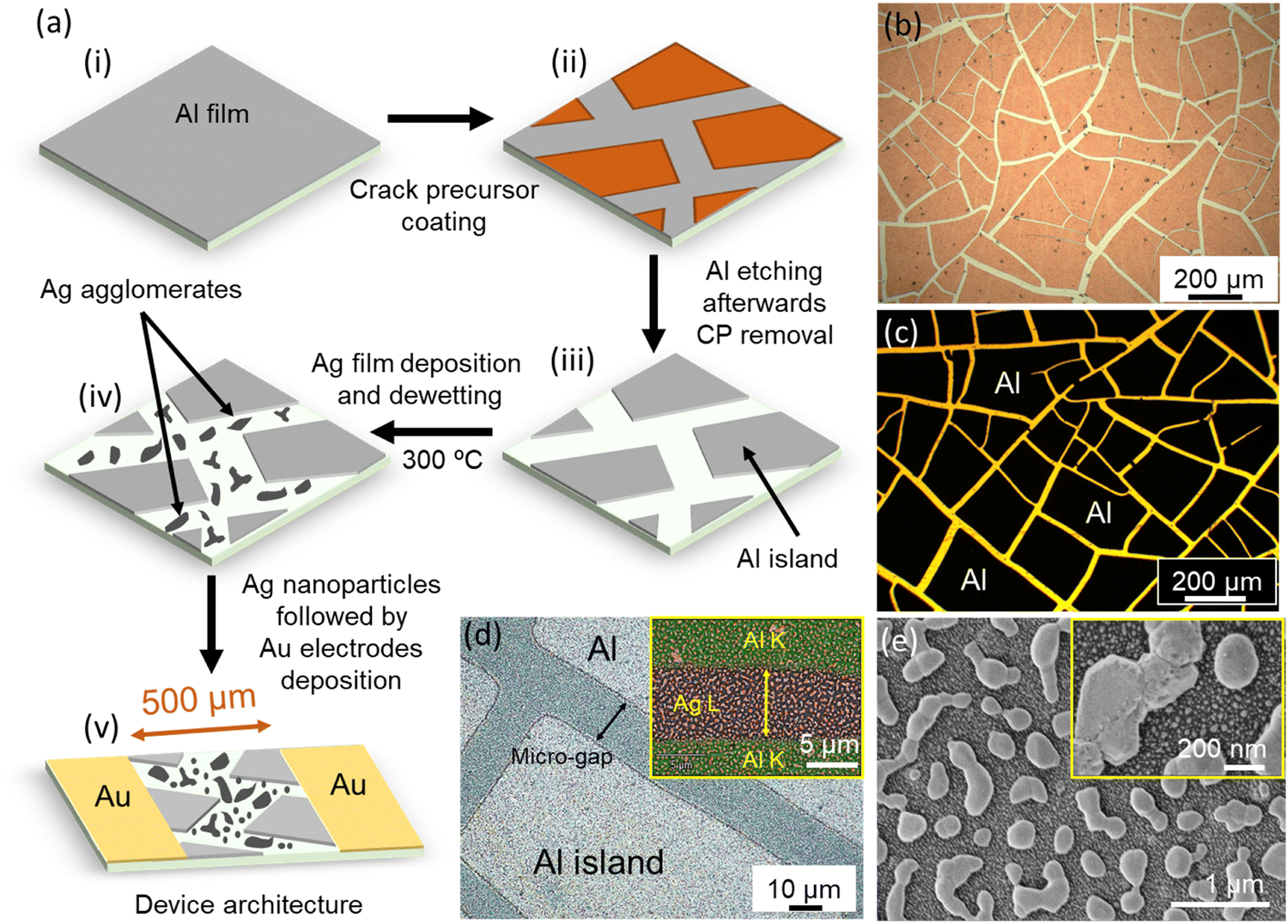 | ||
| Fig. 1 (a) Schematic of steps involved in the device fabrication, (b) optical microscopy image (reflection mode) of a crack template on a Al film/glass substrate, (c) optical microscopy image (transmission mode) of the glass substrate showing Al islands (dark) separated by the interconnected network of micro-gaps (termed as c-Al) resembling the crack pattern (bright yellow), (d) optical micrograph (reflection mode) showing dewetted Ag in the micro-gap regions after the nanoparticle deposition. EDS elemental map in the inset shows Ag L lines (red) in the gap separated by Al K lines of islands (green), and (e) FESEM image from a micro-gap region showing well-separated anisotropic Ag agglomerates with nanoparticles in between as seen in the inset. The images refer to device D1 fabrication. | ||
Fig. 2 deals with I–V characteristics and the associated parameters. During the forward sweep, as the applied voltage increased beyond 48 V, the device D2 (without c-Al, see Fig. 2(a)) switched from the high resistance state (HRS, I ∼ pA) to a low resistance state (LRS), limited by the set compliance, ICC (105 nA, blue curve). This amounts to forming of devices under an applied electric field, Vth (forming) ∼48 V. Such systems with metal nanostructures separated by nanogaps tend to host conducting filaments under the influence of the electric field, often enhanced due to electromigrated atoms forming sharp tips (see Fig. S10, ESI†).8 These connections are only momentary; as the applied voltage is reduced, the filaments retrieve opening up nanogaps, and hence, the device resets back to the HRS (see the red curve in Fig. 2(a)). The Vth value observed from the forming step is somewhat higher; however, the threshold value comes down substantially in the following sweeps to a narrower range of around 10 to 15 V as the accumulated electromigratory metal from repeated sweeps fills the larger gaps (see Fig. S6c and S10, ESI†). It may be observed that in consecutive sweeps, the current increases only gradually with voltage nearly overlapping with other curves till the respective Vth is reached. This current is an additive result of tunnelling processes across the numerous nanogaps present in the active element of the device.
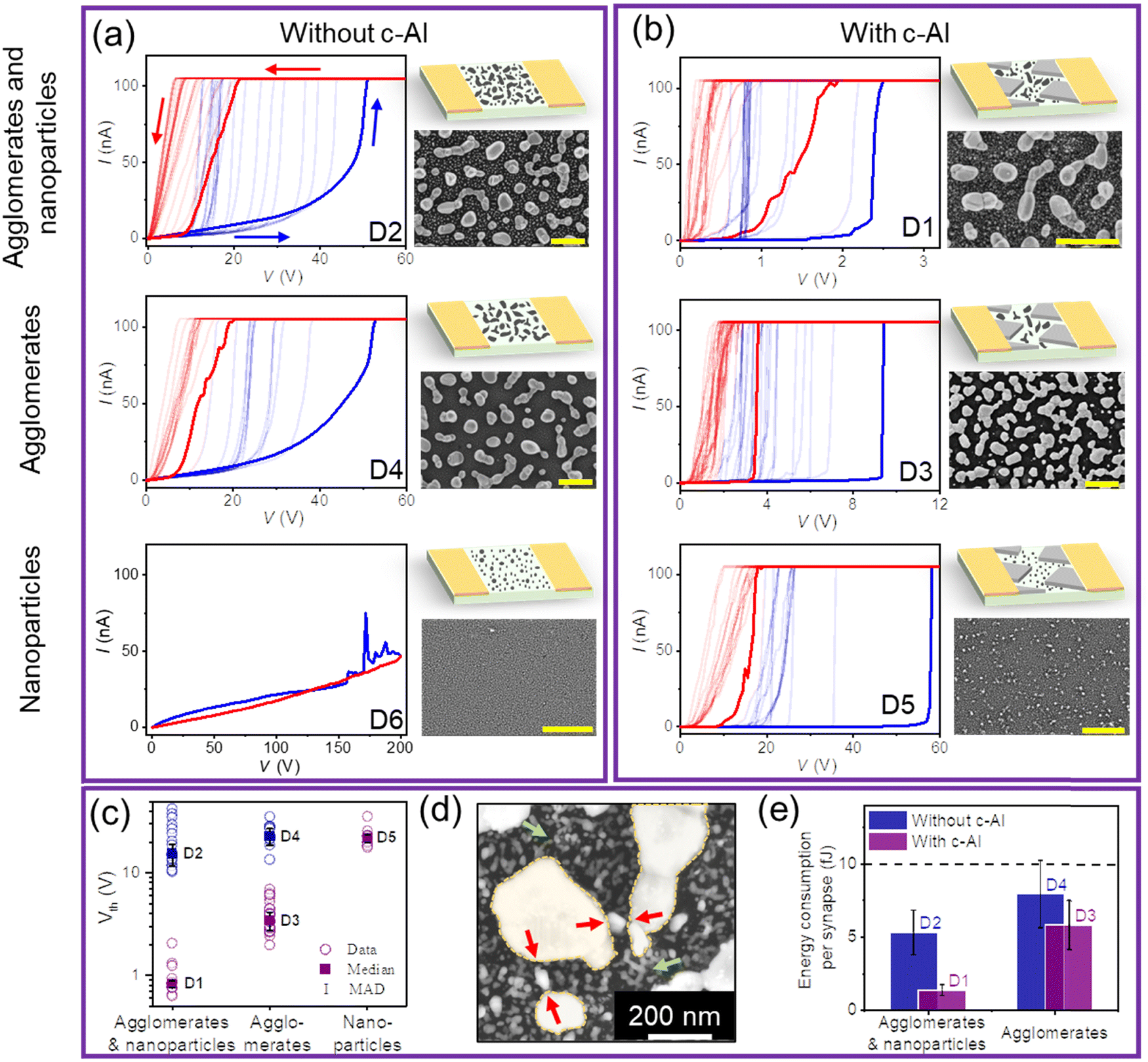 | ||
| Fig. 2 I–V characteristics of devices fabricated without (a), and with (b) c-Al with ICC set at 105 nA (the forming step, dark shade; color saturation increasing with successive sweeps in a narrow voltage range). Schematic of the device architecture along with the corresponding FESEM image (scale bar, 1 μm) is presented on the right. (c) Distribution in the threshold voltage (Vth) values for the control devices, without (blue), and with (purple) c-Al. The median (squares) and median absolute deviation (MAD as error bar) of the experimentally derived Vth data (circle) are also shown. (d) FESEM image of D1 post electrical stress showing outgrowth (red arrows) in nanogaps intervening Ag agglomerates (yellow dash line) emulated as a network of artificial synapses. Green arrows indicate filamentary growth. (e) Energy consumption per synapse. Dashed line stands for a typical value of 10 fJ observed in the case of biological synapses. Device D6 did not show a switching behaviour and is not included. Error bars correspond to the spread in the number of synapses around an agglomerate (see Fig. S13 and S14, ESI† for details). | ||
Unlike D2, the device D1 with a hierarchical c-Al/Ag agglomerate/Ag nanoparticle structure exhibited an abrupt resistive switching when the forming voltage exceeds ∼2.35 V (Fig. 2(b)). It is striking that this value is ∼20 times lower compared to that in the case of D2, without c-Al. However, in spite of the presence of c-Al, D3 exhibits higher forming (9.3 V) and switching voltages, 4 to 6.5 V, clearly due to the absence of Ag nanoparticles that enable facile filament formation. The important role of the agglomerates becomes apparent while referring to D5 (only nanoparticles in between Al islands), where the forming and switching voltages are way higher being in the range of tens of volts. Similar is the scenario with D4 and D6 in the absence of intervening Al islands. D6 without c-Al as well as Ag agglomerates simply failed to exhibit a resistive switching behavior. Indeed, the switching behavior and the associated Vth values play a decisive role in defining the pulsing conditions to be used for a neuromorphic device. The above observations are captured in Fig. 2(c). Device D1 with Ag agglomerates and nanoparticles present in c-Al exhibits a low Vth with a narrow spread, as indicated by its median absolute deviation (MAD) value. However, in the absence of c-Al in D2, not only its Vth is high, the MAD value is also higher, indicating a larger Vth spread. It is evident that the Vth value is significantly higher in all the devices without the c-Al structure, even in the presence of Ag nanostructures. A similar trend is also observed with the forming voltage, as depicted in Fig. S11 (ESI†). Conductive AFM images of D1 in HRS clearly show a high conduction path offered by c-Al facilitating Ag filament formation in the micro-gap regions at such low Vth (see Fig. S12, ESI†). Wu et al. have shown the growth of Ag filaments under a constant voltage bias of 30 V in a planar device with Ag–Al electrodes where the active element was a hybrid layer of Al2O3 nanoparticle arrays in a polyimide (PI) matrix across an active area ∼1.8 × 105 μm2.42 This may be compared with the present study which employs more than 30 times lesser Vth (0.82 V) for the device active area nearly 14 times higher (25 × 105 μm2)! Other literature values from Ag filament based two-terminal devices are listed in Table S1 (ESI†).
The device architecture bears a resemblance to the biological neural network where Ag agglomerates could be considered as spatially distributed neurons and the nanogaps separating them as the synapses (see Fig. 2(d) and Fig. S10d, ESI†). Under the effect of an electric field, Ag nanoparticles tend to form filamentary structures while the agglomerates deform into protrusions (see red and green markings in Fig. 2(d)). The resulting connections could be considered as information transmission pathways similar to biological synapses. The energy required to form such filamentary connections is derived from the analysis detailed in Fig. S13 and S14 (ESI†). Energy consumption per synapse is shown in Fig. 2(e) for devices D1–D4, and the values are comparable with the typical value per synaptic event in biological systems.43 Device D1 having a hierarchical c-Al/Ag agglomerate/Ag nanoparticle structure exhibits the lowest value of energy consumption per synapse, ∼1.3 fJ. Thus, D1 with a hierarchical active element has much to offer. In neuromorphic systems, the conduction paths are generally filamentary and highly dynamic in nature and for their retention, the contact electrodes are to be in close proximity, which not only brings restrictions on device geometry (top contacts versus in-plane) but also on the size of the active volume (area) of the device. Larger device volumes (area) also demand higher threshold voltages. In c-Al, the presence of Al islands interlacing the network of gaps filled with Ag nanostructures plays a crucial role in keeping the parameters under check.
The setup used for measuring the temporal characteristics of the device D1 is shown in Fig. 3(a). The voltage pulse train consisted of 10 or 20 pulses (total time, tp, 1.48 and 3.09 s, respectively) with magnitude VP of 1 V, width, tw and interval, ti of 50 ms each, riding on a constant reading voltage VR of 10 mV, such that during pulsing, the device switches to LRS limited by the set ICC (also see Fig. S15, ESI†). The Ag filament formation and percolative conduction in LRS (see the dashed red line in Fig. 3(a)) as allowed by the set ICC was monitored in terms of rise in conductance, G, of the device (see Fig. 3(b)). Beyond the pulse duration, the sustenance of G would critically depend on the strength of the filaments formed. Accordingly, for low ICC values (0.25 to 0.75 μA, see Fig. 3(c)), the rise in G is found to be quite gradual and non-monotonous, while the same becomes relatively steady and steeper with increasing ICC (1 to 5 μA). With further increase in ICC (30 to 300 μA, see Fig. 3(d)), the rise is not only abrupt but is also noticeably much higher (∼50 to 300 μS) even with a lesser number of pulses (from 20 to 10) (also see Fig. S16, ESI†). The number of pulses was reduced not to overburden the device with electrical stress.
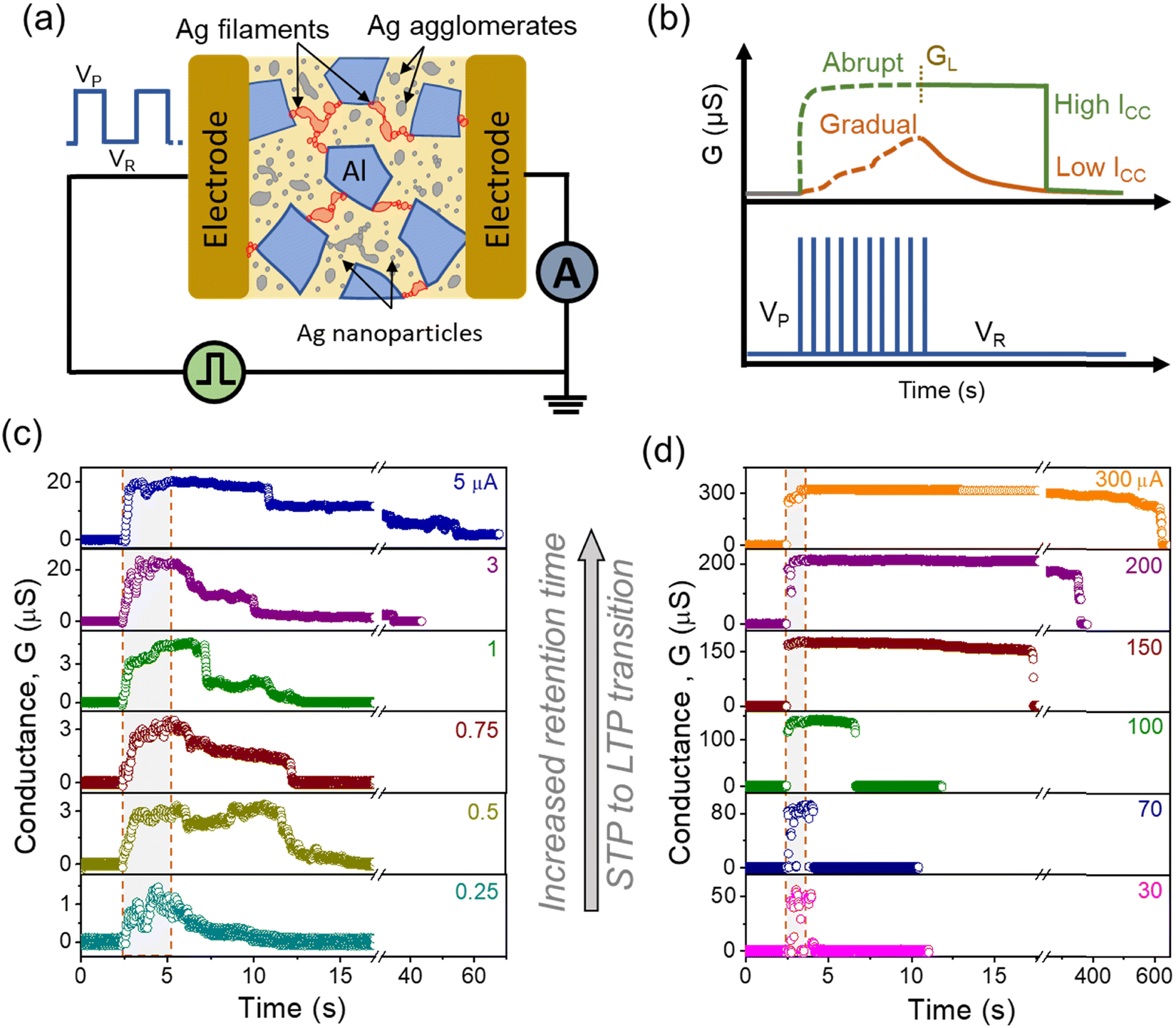 | ||
| Fig. 3 (a) Schematic of the measurement setup adopted for device D1. Square pulses (VP) are applied over a constant reading voltage, VR and the conductance of the device, G, is measured against VR. The active element consists of Ag nanostructures (grey) connecting the c-Al islands (blue) through filamentary paths (red). (b) Representation of variations in G in response to a voltage pulse train under low or high ICC values. In the lower ICC range (c), a gradual rise in G is seen, while for the higher range (d), an abrupt variation is dominant. GL denotes the G value attained at the end of pulsing. Dashed boxes mark the duration of the voltage pulse train (VP ∼ 1 V, VR ∼ 10 mV, 50 ms width and interval, 20 pulses in c and 10 in d). Increased conductance and retention with increasing ICC signify STP to LTP transition. | ||
Besides the strength, the ICC value also determines the life of the filaments. The G value attained at the end of pulsing, GLanuch or briefly GL, is a cumulative effect of filament formation, connectivity, and breakage. While its magnitude stands for the number and strengths of the filamentary connections formed, the longevity measured as the retention time (tr) signifies the degree of potentiation in the context of the neuromorphic action. For low ICC values, GL is small, typically ∼1 to 3 μS, and the G retention is limited up to a few seconds only, and the curve being quite bumpy. This time domain may be referred to as short-term potentiation (STP). For ICC of a few μA, we see an overall improvement in GL and also in G behavior during retention, which is much more pronounced for tens and hundreds of μA of ICC. Thus, the change in the behavior of GL from being gradual and small to becoming steep and high, and the accompanying changes in the tr behavior (from a few seconds to a few minutes) together mark the STP–LTP transition.
We have made a detailed analysis of the G profile in order to gain a better understanding of how the building up of the profile during pulsing influences the profile during retention (beyond pulsing) observed at different ICC values. For this purpose, GL (Fig. 4(a)) and tr (Fig. 4(b)) are plotted as a function of total electrical energy E, calculated as ICC × VP × tp, imparted to the device. The GL value increases nearly linearly at lower electrical stresses (∼0.8 to 9.3 μJ) and then remains somewhat constant (∼20 μS) up to 31 μJ and tends to increase again. Almost concomitantly, the tr value is seen undergoing similar changes in the range ∼1 to 104 μJ. The dip in values seen towards the end may arise due to the instability of weak filaments and may have some contribution from the decrease in the length of the pulse train (20 to 10 pulses). Beyond this range, the increase in tr is steep, ranging to a few minutes. Interestingly, this turn-around behavior at ∼100 μJ corresponds roughly to GL reaching the quantum conductance value (G0 ∼ 77.5 μS) (see the dashed blue line, Fig. 4(a)). The schematic in Fig. 4(d) illustrates the nature of events possibly at play in the device active elements, c-Al/Ag agglomerates/Ag nanoparticles. For a device in HRS, the observed conductance, albeit being low, is cumulative of all tunnelling across nanogap junctions present in the active element. With the electrical stress inducing filamentary growth into the junction regions, the gaps are effectively reduced, giving rise to a steady increase in conductance, monitored as GL. With increasing ICC, this value reaching a plateau (at ∼20 μS) while the tr value dropping are indicative of some junctions getting excessively annealed. However, a further increase in ICC establishes direct contacts, including the possibility of atomic contacts exhibiting quantum conductance. In this sense, in the present device, the STP regime is dominated by potentiation via tunnelling junctions, while LTP involves current flow through direct contacts, which is in line with the literature.13
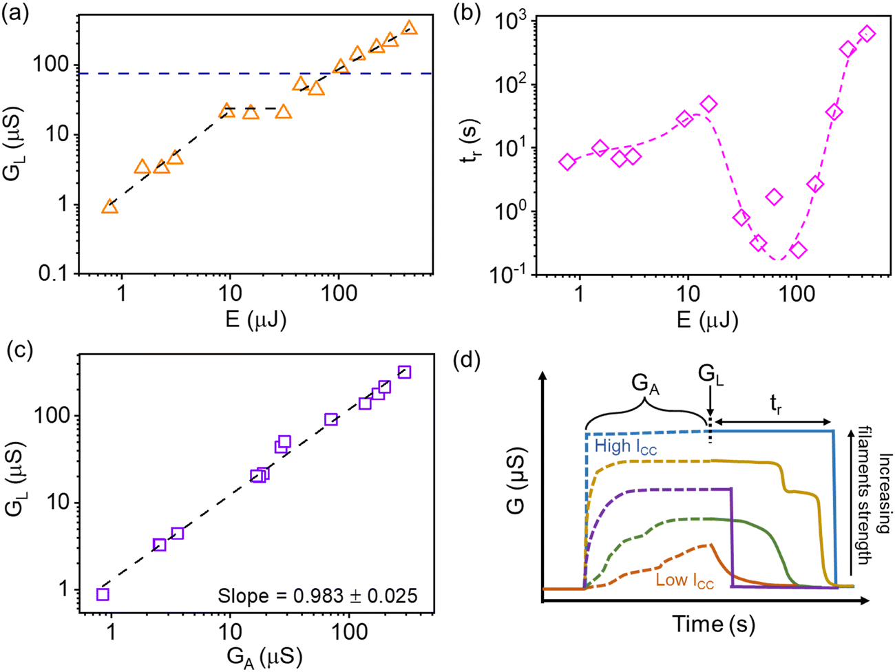 | ||
| Fig. 4 Analysis of the G profile. (a) Variation of GL, and (b) tr as a function of the electrical energy stress (E) on the device. (c) Variation of GL with GA. (d) Schematic of a typical G profile (G evolution during pulsing and retention after pulsing) visualised at different ranges of ICC under similar pulsing conditions (VP ∼ 1 V, VR ∼ 10 mV, ti and tw ∼ 50 ms). | ||
The building up of the G profile during pulsing is captured here as the average of the G profile values collected during the pulse train period, GAverage or briefly GA. As shown in Fig. 4(c), GL varies just as GA itself over a wide range (0.8 to 292 μS). Thus, the GA value provides an insight into how the G profile builds up utilising the underlying nanostructure guided by the pulsing conditions. Electrical pulsing induces atomic electromigration resulting in filamentary growth into tunnel gaps,44 while the accompanying Joule heating may lead to annealing or even breaking of the contacts.45 With higher ICC (>70 μA), the filamentary connections can come live with initial pulses only leading to a steep rise in G and its saturation, which may continue till the pulse train is completed (see schematic, Fig. 4(d)). Thus, its GA would come close to GL. How the G profile reaching saturation early on, may influence tr will be discussed in the next section.
Both ICC and pulse characteristics decide the nature of filamentary paths and, in turn, the time profile of the conductance (G-profile). Accordingly, G profile data were collected (on another D1 device) at different ICC values (0.5 to 20 μA) and at each value, the number of pulses was varied (Np, 5 to 60), while keeping other parameters fixed. In the example data set with ICC of 0.5 μA shown in Fig. S17 (ESI†), the G rise is quite non-monotonous and so is the decay, the GL value being quite low (less than 3 μS) even at high NP. During consecutive acquisitions under similar pulsing conditions, the device was allowed to relax back to HRS after its retention, so as to avoid any remnant effect. Fig. 5(a) shows how at a given ICC value, GA increases with increasing NP, nearly linear for all ICC values except at 20 μA, where G saturates early (NP, 20). The estimation of GA from G profiles is detailed in Fig. S18 (ESI†). The influence of Np on GA is evident from the plot of the slopes of the GA–Np linear fits versus ICC shown in Fig. 5(b). The variation is exponential with the applied pulse, having contributions from the formation of new filaments and strengthening of the existing set of filaments.
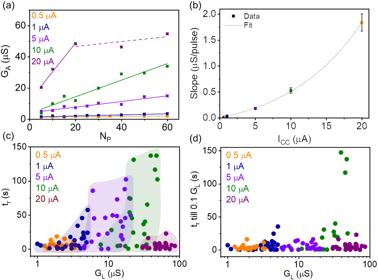 | ||
| Fig. 5 Building up of the G profile. (a) Variation of GA with Np for different ICC. (b) Slopes from the linear fits in (a) as a function of ICC. For 20 μA ICC, the slope refers to the first three data points before G saturates. GL and tr relation. (c) Variations in tr with GL for different ICC. Free-form shapes enclose the individual sets of data where the data spread is due to varied NP (5 to 60). (d) tr of G till 0.1GL (i.e., 90% drop of GL) as a function of GL. (VP ∼ 2 V, VR ∼ 30 mV) (tw and ti ∼ 50 ms). | ||
Further, we have analysed the data by plotting tr against GL, as depicted in Fig. 5(c). The data points fall into different groups (see shaded regions) based on the ICC values. At 5 μA of ICC, tr varies from a few seconds to tens of seconds and GL from ∼7 to 17 μS indicated by the violet band. The range of tr gradually enhanced to a few hundreds of seconds, and GL from ∼10 to 40 μS at higher ICC of 10 μA, respectively. The trend of tr with GL indicates potentiation with increasing ICC. However, tr drops to a few seconds at 20 μA of ICC, indicating some filament fatigue, possibly from an overdose of electrical stress. The behaviour of tr with GL is similar to what is observed in Fig. 4(b), suggesting a low effect of NP variations on the G profile behaviour compared to ICC (refer to Fig. 4(d)). Apart from the complete decay of GL indicated by tr, the initial decay of GL at different ranges of ICC (see Fig. 4(d)) could also be significant in the context of fine grading of plasticity beyond roughly categorising as STP and LTP, as often the initial decay could be much faster. For this purpose, we chose the tr value corresponding to G reaching 90% of the GL value (in other words, tr measured till G ∼ 0.1 GL) as a representative figure and plotted it as a function of GL for different ICC (see Fig. 5(d)). It is observed that for all ICC till 20 μA, G drops to 0.1 of the corresponding GL within ∼50 seconds, while rest of the decay may prolong as seen with the total tr variation in Fig. 5(c). However, for 10 μA ICC, some data points of G decaying to 0.1 GL took up to 150 seconds, which indicates that the electrical stress is strong enough to cause significant potentiation but not to burn the filaments.
Fig. 6 depicts a plot relating the building up of the G profile during pulsing in the form of GA with the final state attained at the end of pulsing as GL. It is remarkable that the data points from all the ICC and the NP value studies are spread around the linear relationship of GL with GA (see the green band, Fig. 6), suggesting a scale-free temporal correlation between the two quantities. The spread of GL becomes narrower with increasing ICC as the strengths of the filaments improve.
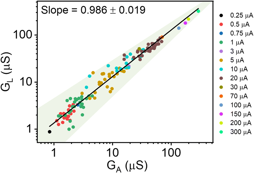 | ||
| Fig. 6 Correlation of GL with GA of the G profile with varied Np in the ICC range of 0.25 to 300 μA. Data are sourced from Fig. 4 and 5. | ||
A discussion of the above results is worthwhile. The I–V characteristics in Fig. 2 highlight the role of c-Al in effectively reducing Vth and in turn, the energy consumption per synapse of the ASN. The polygon-shaped Al islands intensify the local electric field at regions with high curvatures, which may guide the facile filamentary growth (refer to Fig. S12, ESI†), similar to the one reported by Boland and co-workers for activating the Ag nanowire network by varying the electrode shape.46 The nature of Ag filaments formed during pulsing can broadly explain the observed G behaviour. The gradual and bumpy G profile (GL, 1 – 3 μS) with pulses indicates thin filamentary growth in tunnel gaps at play, which get strengthened and extend further with GL (up to 20 μS), followed by non-monotonically decaying G as the structures relax. An abrupt and sturdy profile with initial pulses only, at GL above G0, marks the formation of stable thick filaments which may not build up with further pulses and whose G retention is usually steady and lasts longer. These two scenarios can be easily identified at low and high ICC in the schematic presented in Fig. 4(d), and also the ICC or NP determining the filamentary growth is widely reported in the ECM literature.7,12,13,47 The turnover of the G profile from gradual towards steeper with ICC may facilitate the filament density, but excessive electrical stress ends up annihilating them due to low ampacity expected of thin filaments, which results in a step in GL along with significantly low tr. Saturation of GA beyond 20 pulses in Fig. 5(a) can also be related to a similar phenomenon. The tr bands in Fig. 5(c) are seen to be overlapping in some regions of GL, indicating iso-G states which could be achieved by manipulating the combination of filament density and strength.12 However, a detailed in situ microscopic investigation is to be carried out to gain further insight into the influence of pulse characteristics on behaviour of the G profile in a hierarchical structure-based ASN. The current device features the short-term plasticity over a wide GL range (see Fig. 5(d)), which is the basis of various cognitive activities.48 Tunable relaxation behaviour of ASN with volatility could be utilised for complex computing tasks employing a neuromorphic approach and hardware security.49,50 We believe that developing ASN devices in close resemblance to the biological brain would allow us to understand the complex mechanism of cognitive learning emerging from the plasticity of a network of synapses. The futuristic scope of the work could be relating to emulating complex associative learning wherein the c-Al islands will be exploited as input electrodes to feed different stimuli simultaneously as multiple sensory signals.
4. Conclusions
In conclusion, we have been able to form hierarchical Al structures using a simple, cost-effective crack template and exploited the interconnected cracks with hierarchical Ag nanostructures successfully for emulating synaptic plasticity in the neuromorphic context. Importantly, the whole architecture is based on self-forming methods, and with this design principle, the active element can be spread over an indefinitely large area. Vth of fabricated control devices highlights the importance of c-Al and Ag nanostructures in minimising the energy consumption per synapse. The electric field enhancement by c-Al guides the growth of metallic filaments enabling facile control and tunability over a wide range of ICC. The effect of electrical energy spent on building up of the G profile following its decay was analysed in terms of GA, GL, and tr, and correlated with the nature of filaments. Exponential potentiation of GA per pulse with ICC further shed light on the evolution of filamentary paths with pulsing conditions. STP and LTP were shown to be originating from conduction through tunnelling junctions and ohmic contacts with reference to G0. Scale-free correlation of GL with GA shown over a wide G range could be a model for building biologically plausible self-formed hierarchical structure-based neuromorphic devices. Furthermore, the present architecture with large Al islands is highly advantageous in that the islands may serve as contact pads to introduce external signals from say, sensors, into the neuromorphic circuitry. As the network of self-formed Al islands can be extended indefinitely, the fabrication needs not be limited to small areas.Data availability
The data that support the findings of this study are available from the corresponding author upon reasonable request.Author contributions
Rohit Attri: data curation, formal analysis, investigation, methodology, writing – original draft, and writing – review and editing; Indrajit Mondal: conceptualization, formal analysis, validation, and writing – review and editing; Bhupesh Yadav: methodology; G. U. Kulkarni: conceptualization, formal analysis, funding acquisition, investigation, methodology, project administration, resources, supervision, validation, visualization, and writing – review and editing; and C. N. R. Rao: supervision and writing – review and editing.Conflicts of interest
The authors declare no conflict of interest.Acknowledgements
The authors acknowledge the financial support from the Department of Science and Technology (DST), India and Jawaharlal Nehru Centre for Advanced Scientific Research (JNCASR), Bengaluru for the research facilities. Rohit Attri and I. M. thank JNCASR for the fellowship. B. Y. acknowledges CSIR for the fellowship.References
- J. Tang, F. Yuan, X. Shen, Z. Wang, M. Rao, Y. He, Y. Sun, X. Li, W. Zhang, Y. Li, B. Gao, H. Qian, G. Bi, S. Song, J. J. Yang and H. Wu, Adv. Mater., 2019, 31, 1902761 CrossRef CAS PubMed.
- S. Choi, J. Yang and G. Wang, Adv. Mater., 2020, 32, 2004659 CrossRef CAS PubMed.
- Q. Wan, M. T. Sharbati, J. R. Erickson, Y. Du and F. Xiong, Adv. Mater. Technol., 2019, 4, 1900037 CrossRef.
- J. Zhu, T. Zhang, Y. Yang and R. Huang, Appl. Phys. Rev., 2020, 7, 011312 CAS.
- Z. Wang, M. Rao, R. Midya, S. Joshi, H. Jiang, P. Lin, W. Song, S. Asapu, Y. Zhuo, C. Li, H. Wu, Q. Xia and J. J. Yang, Adv. Funct. Mater., 2018, 28, 1704862 CrossRef.
- W. Wang, M. Wang, E. Ambrosi, A. Bricalli, M. Laudato, Z. Sun, X. Chen and D. Ielmini, Nat. Commun., 2019, 10, 1–9 CrossRef PubMed.
- M.-K. Kim and J.-S. Lee, ACS Nano, 2018, 12, 1680–1687 CrossRef CAS PubMed.
- Z. Wang, S. Joshi, S. E. Savel’ev, H. Jiang, R. Midya, P. Lin, M. Hu, N. Ge, J. P. Strachan, Z. Li, Q. Wu, M. Barnell, G. L. Li, H. L. Xin, R. S. Williams, Q. Xia and J. J. Yang, Nat. Mater., 2017, 16, 101–108 CrossRef CAS PubMed.
- S. A. Chekol, S. Menzel, R. Waser and S. Hoffmann-Eifert, Adv. Electron. Mater., 2022, 8, 2200549 CrossRef CAS.
- S. A. Chekol, S. Menzel, R. W. Ahmad, R. Waser and S. Hoffmann-Eifert, Adv. Funct. Mater., 2022, 32, 2111242 CrossRef CAS.
- F. Ye, F. Kiani, Y. Huang and Q. Xia, Adv. Mater., 2022, 2204778 Search PubMed.
- S. La Barbera, D. Vuillaume and F. Alibart, ACS Nano, 2015, 9, 941–949 CrossRef CAS PubMed.
- T. Ohno, T. Hasegawa, T. Tsuruoka, K. Terabe, J. K. Gimzewski and M. Aono, Nat. Mater., 2011, 10, 591–595 CrossRef CAS PubMed.
- K. Krishnan and S. Vijayaraghavan, Adv. Electron. Mater., 2022, 8, 2200509 CrossRef CAS.
- X. Yan, J. H. Qian, V. K. Sangwan and M. C. Hersam, Adv. Mater., 2022, 34, 2108025 CrossRef CAS PubMed.
- Z. Wang, S. Joshi, S. Savel’ev, W. Song, R. Midya, Y. Li, M. Rao, P. Yan, S. Asapu, Y. Zhuo, H. Jiang, P. Lin, C. Li, J. H. Yoon, N. K. Upadhyay, J. Zhang, M. Hu, J. P. Strachan, M. Barnell, Q. Wu, H. Wu, R. S. Williams, Q. Xia and J. J. Yang, Nat. Electron., 2018, 1, 137–145 CrossRef.
- S. Ambrogio, P. Narayanan, H. Tsai, R. M. Shelby, I. Boybat, C. di Nolfo, S. Sidler, M. Giordano, M. Bodini, N. C. P. Farinha, B. Killeen, C. Cheng, Y. Jaoudi and G. W. Burr, Nature, 2018, 558, 60–67 CrossRef CAS PubMed.
- M. K. Song, J. H. Kang, X. Zhang, W. Ji, A. Ascoli, I. Messaris, A. S. Demirkol, B. Dong, S. Aggarwal, W. Wan, S. M. Hong, S. G. Cardwell, I. Boybat, J. S. Seo, J. S. Lee, M. Lanza, H. Yeon, M. Onen, J. Li, B. Yildiz, J. A. Del Alamo, S. Kim, S. Choi, G. Milano, C. Ricciardi, L. Alff, Y. Chai, Z. Wang, H. Bhaskaran, M. C. Hersam, D. Strukov, H. P. Wong, I. Valov, B. Gao, H. Wu, R. Tetzlaff, A. Sebastian, W. Lu, L. Chua, J. J. Yang and J. Kim, ACS Nano, 2023, 17(13), 11994–12039 CrossRef CAS PubMed.
- Q. Xia and J. J. Yang, Nat. Mater., 2019, 18, 309–323 CrossRef CAS PubMed.
- G. C. Adam, A. Khiat and T. Prodromakis, Nat. Commun., 2018, 9, 5267 CrossRef CAS PubMed.
- C. W. Lynn and D. S. Bassett, Nat. Rev. Phys., 2019, 1, 318–332 CrossRef.
- A. Z. Stieg, A. V. Avizienis, H. O. Sillin, C. Martin-Olmos, M. Aono and J. K. Gimzewski, Adv. Mater., 2012, 24, 286–293 CrossRef CAS PubMed.
- B. Bannur and G. U. Kulkarni, Mater. Horiz., 2020, 7, 2970–2977 RSC.
- A. Z. Stieg, A. V. Avizienis, H. O. Sillin, C. Martin-Olmos, M.-L. Lam, M. Aono and J. K. Gimzewski, Jpn. J. Appl. Phys., 2014, 53, 01AA02 CrossRef CAS.
- M. Aono and K. Ariga, Adv. Mater., 2016, 28, 989–992 CrossRef CAS PubMed.
- Q. Li, A. Diaz-Alvarez, R. Iguchi, J. Hochstetter, A. Loeffler, R. Zhu, Y. Shingaya, Z. Kuncic, K. Uchida and T. Nakayama, Adv. Funct. Mater., 2020, 30, 1–11 Search PubMed.
- G. Milano, G. Pedretti, M. Fretto, L. Boarino, F. Benfenati, D. Ielmini, I. Valov and C. Ricciardi, Adv. Intell. Syst., 2020, 2, 2000096 CrossRef.
- H. Tanaka, M. Akai-Kasaya, A. TermehYousefi, L. Hong, L. Fu, H. Tamukoh, D. Tanaka, T. Asai and T. Ogawa, Nat. Commun., 2018, 9, 2693 CrossRef PubMed.
- D. Banerjee, T. Kotooka, S. Azhari, Y. Usami, T. Ogawa, J. K. Gimzewski, H. Tamukoh and H. Tanaka, Adv. Intell. Syst., 2022, 4, 2100145 CrossRef.
- J. B. Mallinson, S. Shirai, S. K. Acharya, S. K. Bose, E. Galli and S. A. Brown, Sci. Adv., 2019, 5, 1–8 Search PubMed.
- S. Shirai, S. K. Acharya, S. K. Bose, J. B. Mallinson, E. Galli, M. D. Pike, M. D. Arnold and S. A. Brown, Netw. Neurosci., 2020, 4, 432–447 CrossRef PubMed.
- N. Carstens, B. Adejube, T. Strunskus, F. Faupel, S. Brown and A. Vahl, Nanoscale Adv., 2022, 4, 3149–3160 RSC.
- Y. Yang, B. Chen and W. D. Lu, Adv. Mater., 2015, 27, 7720–7727 CrossRef CAS PubMed.
- U. S. Goteti and R. C. Dynes, J. Appl. Phys., 2021, 129, 073901 CrossRef CAS.
- C. S. Dunham, S. Lilak, J. Hochstetter, A. Loeffler, R. Zhu, C. Chase, A. Z. Stieg, Z. Kuncic and J. K. Gimzewski, J. Phys. Complex., 2021, 2, 042001 CrossRef.
- B. Bannur, B. Yadav and G. U. Kulkarni, ACS Appl. Electron. Mater., 2022, 4, 1552–1557 CrossRef CAS.
- B. Yadav, I. Mondal, B. Bannur and G. U. Kulkarni, Nanotechnology, 2024, 35, 015205 CrossRef PubMed.
- T. S. Rao, I. Mondal, B. Bannur and G. U. Kulkarni, Discover Nano, 2023, 18, 124 CrossRef PubMed.
- K. D. M. Rao, R. Gupta and G. U. Kulkarni, Adv. Mater. Interfaces, 2014, 1, 1–7 CAS.
- I. Mondal, G. Bahuguna, M. K. Ganesha, M. Verma, R. Gupta, A. K. Singh and G. U. Kulkarni, ACS Appl. Mater. Interfaces, 2020, 12, 54203–54211 CrossRef CAS PubMed.
- A. Kumar and G. U. Kulkarni, J. Appl. Phys., 2016, 119, 015102 CrossRef.
- C. Wu, T. W. Kim, T. Guo, F. Li, D. U. Lee and J. J. Yang, Adv. Mater., 2017, 29, 1602890 CrossRef PubMed.
- D. Kuzum, S. Yu and H.-S. Philip Wong, Nanotechnology, 2013, 24, 382001 CrossRef PubMed.
- W. Sun, B. Gao, M. Chi, Q. Xia, J. J. Yang, H. Qian and H. Wu, Nat. Commun., 2019, 10, 3453 CrossRef PubMed.
- J. Aeschlimann, F. Ducry, C. Weilenmann, J. Leuthold, A. Emboras and M. Luisier, Phys. Rev. Appl., 2023, 19, 024058 CrossRef CAS.
- J. A. Fairfield, C. Ritter, A. T. Bellew, E. K. McCarthy, M. S. Ferreira and J. J. Boland, ACS Nano, 2014, 8, 9542–9549 CrossRef CAS PubMed.
- H. Sun, Q. Liu, C. Li, S. Long, H. Lv, C. Bi, Z. Huo, L. Li and M. Liu, Adv. Funct. Mater., 2014, 24, 5679–5686 CrossRef CAS.
- C. Li, X. Zhang, P. Chen, K. Zhou, J. Yu, G. Wu, D. Xiang, H. Jiang, M. Wang and Q. Liu, iScience, 2023, 26, 106315 CrossRef CAS PubMed.
- R. Wang, J.-Q. Yang, J.-Y. Mao, Z.-P. Wang, S. Wu, M. Zhou, T. Chen, Y. Zhou and S.-T. Han, Adv. Intell. Syst., 2020, 2, 2000055 CrossRef.
- D. Kim, B. Jeon, Y. Lee, D. Kim, Y. Cho and S. Kim, Appl. Phys. Lett., 2022, 121, 010501 CrossRef CAS.
Footnote |
| † Electronic supplementary information (ESI) available: Figures supporting main text. See DOI: https://doi.org/10.1039/d3mh01367g |
| This journal is © The Royal Society of Chemistry 2024 |