
 Open Access Article
 This Open Access Article is licensed under a
 Creative Commons Attribution 3.0 Unported Licence
Slot-die coating of electron transport layers for perovskite solar cells using water and butanol-based tin oxide dispersions†
Anuja
Vijayan
a,
Vishnu
Vijayakumar
a,
Malin B.
Johansson
 a,
Masoud
Karimipour
b,
Monica
Lira-Cantu
b,
Byeong Jo
Kim
a and
Gerrit
Boschloo
*a
a,
Masoud
Karimipour
b,
Monica
Lira-Cantu
b,
Byeong Jo
Kim
a and
Gerrit
Boschloo
*a
aDepartment of Chemistry – Angstrom Laboratory, Physical Chemistry, Box 523, Uppsala University SE-751 20, Uppsala, Sweden. E-mail: gerrit.boschloo@kemi.uu.se
bCatalan Institute of Nanoscience and Nanotechnology (ICN2), CSIC and the Barcelona Institute of Science and Technology (BIST), Building ICN2, Campus UAB, E-08193 Bellaterra, Barcelona, Spain
First published on 9th April 2024
Abstract
Lead halide perovskite photovoltaics have shown an impressive efficiency increase over the past decade. Making this technology industrially viable requires precise optimization of every single deposition step. Here we used slot-die coating, a promising scalable deposition technique to enable large scale deposition. We demonstrate the challenges in developing high-quality slot-die coated tin oxide (SnO2) films, suited as electron selective layers in perovskite solar cells. We studied the film quality of two commercially available colloidal SnO2 dispersions by controlling pump rate, coating speed and temperature of the indium tin oxide substrates (ITO). The water-based dispersion was more difficult to control, but resulted in better perovskite solar cell performance than the butanol-based dispersion. Hysteresis in J–V curves from the water-based tin oxide dispersion was reduced by potassium fluoride addition. A maximum power conversion efficiency of 17.5% was achieved for MAPbI3-based solar cells by careful optimization of the deposition parameters.
Introduction
Lead halide-based perovskite materials are considered one of the most promising materials for developing next-generation solar cells due to their excellent optoelectronic properties.1,2 Over the last decade, continuous advances in device engineering resulted in unprecedented improvements in their power conversion efficiency (PCE) from 3.8% to 26.1%.3–5Due to this excellent performance, interest in the technologies that facilitate the transition from laboratory to industrial scale is growing. For instance, spin coating is a commonly used deposition method, but unsuited for industrial upscaling. Taking perovskite solar cells to an industrial level requires a lot of effort and optimization in upscaling technologies. Therefore, it is important to develop suitable printing methods for each layer of the perovskite solar cell.6,7
The perovskite solar cell device n–i–p stack consists of a glass substrate with a transparent conductive oxide (TCO), electron transport layer (ETL), perovskite layer, p-type hole transport layer (HTL) and metal back contact electrode.8 Carrier-selective ETL and HTL are crucial for extracting and transporting charges, while minimizing the interfacial charge recombination. In an n–i–p configured perovskite solar cell, the perovskite layer is deposited on top of the ETL layer.9 Therefore, the quality and properties of the ETL layer directly affect the properties of the light absorbing perovskite layer. Thus, developing and optimizing the ETL layer has become a hot topic for research.
Initially, TiO2 was widely used as the electron transport layer in perovskite solar cells, owing to its suitable optoelectronic properties. However, it has photocatalytic properties under UV-illumination and requires high temperature annealing of about 500 °C to achieve proper crystallinity, making this material less suitable for use in upscaling and commercialization of PSC.3,10–12 To overcome these drawbacks, alternative n-type metal oxides have been studied, which should allow for low temperature processing, are low in cost and should improve stability.13–17
Among the various alternatives, SnO2 stands out as a very suitable ETL and has gained major attention in recent years.8,18,19 The highest power conversion efficiency for PSC with SnO2 as ETL has reached more than 25%. The SnO2-based ETLs exhibit several qualities which are suitable for solar cells, such as wide bandgap (3.6 eV), good optical transmittance, high charge mobility and compatibility with low temperature processing, all of which make it a good choice as an ETL in PSC.20,21
Low temperature solution-processed SnO2 were first applied as an ETL applied in 2015 by Ke et al.22 The SnO2 layer was prepared from SnCl2·2 H2O by sol–gel method and yielded a power conversion efficiency (PCE) of 17.21%. After the first report research focused on improving the solution processing of SnO2 by tuning precursor composition. The relatively low stability and reliability of sol–gel processed SnO2 led to further research into alternative approaches. A major breakthrough was that Jiang et al. found that a commercial SnO2 colloidal solution could be used to form the ETL. Aqueous SnO2 colloidal solution with 3–4 nm sized SnO2 nanoparticles formed a dense, pinhole free SnO2 film after mild heating, with good transparency, pushing the PSC efficiency to a record value of 25.7%.23 After this breakthrough, commercial water-based SnO2 has been widely used in solar cells with various modification strategies.24–26
Since most of the research has only been focused on spin coating technology for small area solar cell fabrication, which are not easily transferable to upscaling conditions. Galagan et al. demonstrated the feasibly of depositing SnO2 using slot-die coating.27 Smith et al. developed SnO2-nanoparticle deposition with two scalable techniques including slot die coating and achieved power conversion efficiency over 19%.28 Bu et al. reported KOH treatment to SnO2 beneficial for obtaining high performance and hysteresis free device in flexible cells and modules-based slot-die coated SnO2 ETL.29 Recently Richards et al. demonstrated the roll-to-roll (R2R) slot-die coating of the SnO2 ETL by applying the low flow limit to showcase prediction of the processing window for solvent-engineered SnO2.30 Besides slot-die coating, other scalable SnO2 deposition methods for perovskite modules, such as blade coating, screen printing and spray coating have been developed and several issues such as manufacturing costs, intrinsic stability, and reproducibility should be carefully studied.29,31–36
In this work, we exclusively discuss the challenges of the application of two types of commercially available colloidal SnO2 solutions in a benchtop slot die coater. High quality ETL layers are obtained by carefully controlling different parameters such as pump rate, coating speed and temperature, etc. To assess the ETL quality, we completed the fabrication of perovskite solar cells by depositing perovskite and hole transport layers using conventional spin coating and the gold contact by vacuum evaporation.
Results and discussion
In the current study, we selected two commercially available SnO2 colloidal solutions from Alfa Aesar (15 wt% in water) and Avantama (2.5 wt% in 1-butanol). In the aqueous colloid solution the nanoparticles are stabilized by a negative charge and have a size of 3–4 nm.29 In the butanol solution SnO2 nanoparticles (size 7 nm) are stabilized by organic ligands with a phosphate group. From here onwards we refer to the water-based solution as W–SnO2 and butanol based as B–SnO2.To set appropriate operating parameters to obtain a high-quality SnO2 layer for perovskite solar cells, we have systematically controlled the pump rate, coating speed, coating temperature and coating gap. Fig. 1 shows the schematics of the slot-die coating process of SnO2 deposition. Slot-die coating is a non-contact deposition method where the solution is pumped through a syringe to the well-defined slit of the slot-die head unit at a defined pump rate. In the slot-die coater unit, die head is fixed and the substrate holder moves underneath at set speed.
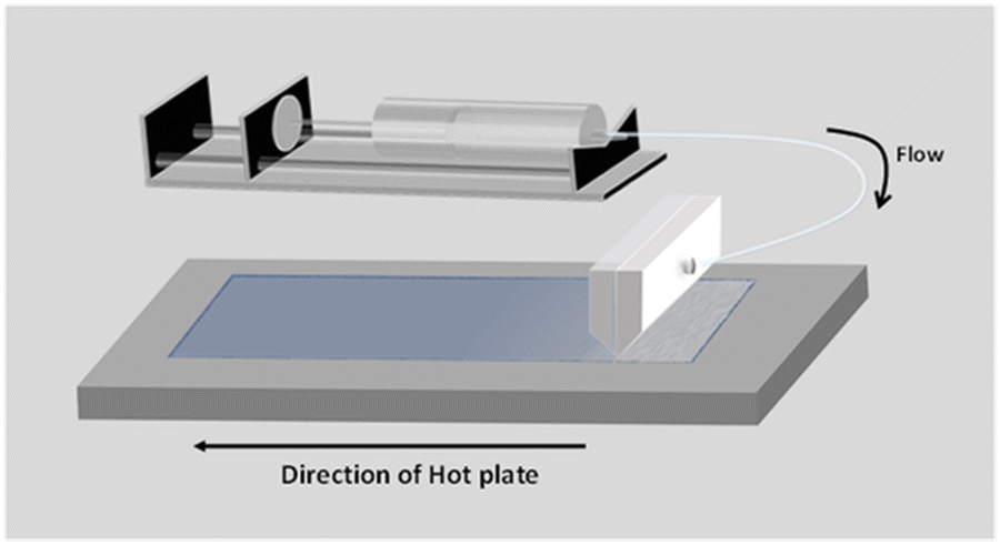 | ||
| Fig. 1 Schematic representation of slot-die coating of SnO2 solution. | ||
The slot die-coater used in this work is placed inside a fume hood. All the film fabrication discussed are done at ambient atmosphere with around 40 to 50% relative humidity. We found that highly uniform SnO2 thin films can be deposited, when the deposition parameters are optimized carefully. Coating was started on a well cleaned ITO-coated glass substrate. Selecting a cleaned substrate for coating plays a crucial role in film formation. We noticed a considerable difference in the contact angle of W–SnO2 on previously cleaned and freshly cleaned substrates (Fig. S1 in ESI†). It is advantageous if the surface is cleaned using deionized (DI) water just before the deposition to increase the wetting of SnO2 solution on ITO substrates. It is worth to note that we didn’t apply any other prior treatments, such as UV-ozone, to improve the surface wetting of ITO before SnO2 deposition.
To deposit SnO2 films of appropriate thickness on ITO, we diluted W–SnO2 with deionized water and B–SnO2 with 1-butanol and adjusted deposition speed and pump rate. The concentration of the W–SnO2 was fixed to 2 wt% and B–SnO2 was fixed to 1.2 wt% to aim for a final film thickness of about 50 nm, which we confirmed from the SEM cross section. (Fig. S2 in ESI†).
Initial optimization stages with water-based W–SnO2 were challenging due to low viscosity (0.890 cp) and high surface tension (72.8 mN m−1) of water, which promote excessive flow and droplet formation/contraction, respectively. We tried to mix water-based solution with isopropanol (IPA) and 1-butanol to increase the viscosity and decrease the surface tension. Since miscibility of butanol in water is very limited, we focused on the addition of IPA. We diluted the W–SnO2 with 1![[thin space (1/6-em)]](https://www.rsc.org/images/entities/char_2009.gif) :1 deionized water and IPA. IPA was added dropwise to the diluted solution to avoid agglomeration of the nanocrystals. Due to the difficulty in producing reproducible film quality with such mixed solvent solutions, we decided to focus on diluting the stock solution with DI water alone.
:1 deionized water and IPA. IPA was added dropwise to the diluted solution to avoid agglomeration of the nanocrystals. Due to the difficulty in producing reproducible film quality with such mixed solvent solutions, we decided to focus on diluting the stock solution with DI water alone.
To obtain uniform, defect-free coatings in a slot-die coating process, the solution should be transferred via the slot-die head to the substrate in a steady state, where the fluid pressure must be balanced in its upstream (from the die head) and downstream (to the substrate). Coating defects such as meniscus break, spreading/leaking of solution and air bubble formation can originate from an unbalanced pressure.
Adjusting the pump rate together with the substrate coating speed, is the best way to control the fluid pressure. As the pump rate is increased, more fluid is forced into the coating bead per unit time, raising the pressure inside the coating bead. Increasing the substrate line speed helps to reduce the pressure of the fluid to some extent. A good balance between pump rate and coating speed must be carefully optimized to obtain high-quality films. To obtain high-quality, uniform, pinhole-free SnO2 layers, we systematically varied the colloid concentration, pump rate, coating speed and the temperature of the hotplate holding the substrate.
Here in, we started controlling the pump rate while keeping all the other parameters constant. The pump rate was varied from 50 μl min−1 to 300 μl min−1 for W–SnO2 and 100 μl min−1 to 300 μl min−1 for B–SnO2. The obtained film quality of W–SnO2 changed drastically with different pump rates. Higher pump rates force more fluid to reach the substrate, which leads to an uncontrolled flow of solution on the substrate, resulting in an uneven film morphology with higher thickness. To make more uniform and reproducible film, we adopted a relatively low pump rate for coating.
On the other hand, B–SnO2 film quality was not affected by the pump rate, see Fig. S3 (ESI†). This difference is attributed to the viscosity of the butanol (3.5 cp), which is higher than that of water (0.89 cp), and its surface tension, which is lower (21 mN m−1vs. 72 mN m−1). The combination of these parameters will promote uniform coating for butanol-based inks, while drop formation and contraction may occur for water-based inks. The optimized slot-die coating parameters for deposition of the two colloidal SnO2 solutions are listed in Table 1. The optimum pump rate for W–SnO2 was found to be 90 μl min−1 with coating speed of 80 cm min−1 and a substrate temperature of 80 °C.
| Pump rate (μl min−1) | Coating speed (cm min−1) | Coating temperature (°C) | Coating gap (μm) | |
|---|---|---|---|---|
| W–SnO2 | 90 | 80 | 80 | 88 |
| B–SnO2 | 200 | 80 | 60 | 100 |
Transmission measurements of SnO2 films on ITO was performed (Fig. 2a) to understand the optical properties. Both B–SnO2 and W–SnO2 show excellent light transmittance in the visible region, which indicates good optical quality of the films. It is observed that the transmittance of the B–SnO2 films in the wavelength range from 350 nm to 450 nm higher than that of W–SnO2. Corresponding images of the slot-die coated SnO2 films are shown in Fig. 2b.
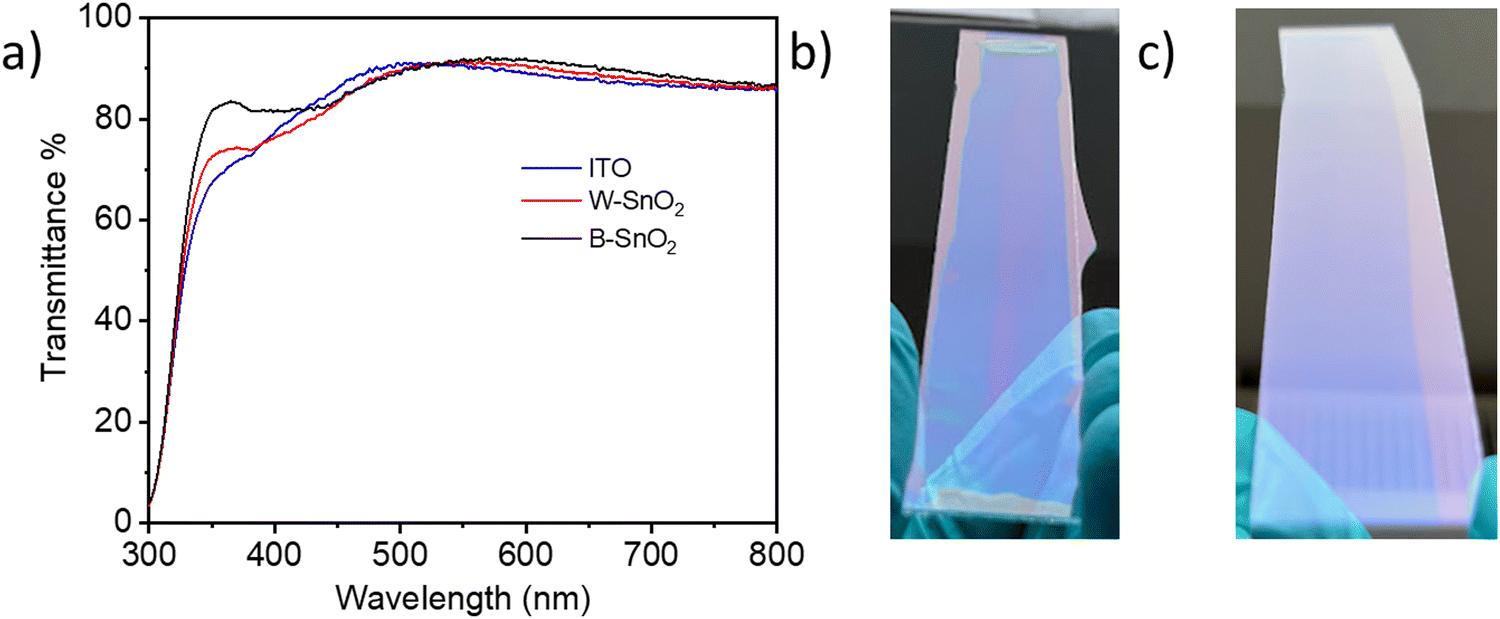 | ||
| Fig. 2 (a) Transmittance spectra of slot die coated SnO2 films on ITO-glass substrates. Photographic images of the corresponding films (14 cm × 3 cm): (b) W–SnO2 (c) B–SnO2. | ||
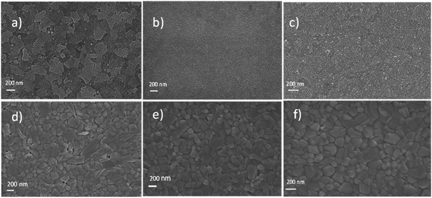 | ||
| Fig. 3 Scanning electron microscopy surface images of (a) ITO substrate (b) W–SnO2 on ITO (c) B–SnO2 on ITO. (d)–(f) MAPbI3 films deposited on (a)–(c) respectively. | ||
Scanning electron microscopy (SEM) was used to study the surface morphology of the two kinds of SnO2 film and compared with the bare ITO substrate. Both W–SnO2 and B–SnO2 films completely covered the ITO and the surface images confirmed uniform film formation as well. Lower magnification images are given in the electronic supplementary information (ESI† Fig. S3).
To study the formation of perovskite on the slot-die coated SnO2 films, we spin coated MAPbI3 perovskite on top of bare ITO substrates, as well as on W–SnO2 and B–SnO2-coated substrates. The average grain size of perovskite crystals was 80–250 nm, which remained the same for both SnO2 films. To deposit the perovskite layer by spin coating, usually prior UV-Ozone treatment is needed, which improves the wetting of the substrates with the perovskite precursor solution. To confirm this effect, contact angle measurements of perovskite precursor on both types of SnO2 films were performed, where 20 min UV-Ozone treatment was applied before perovskite deposition. In the case of W–SnO2, this pretreatment improved the wetting of the perovskite precursor on W–SnO2 the average contact angle of perovskite solution on W–SnO2 was 40.29° without UV-ozone treatment, decreasing to 25.75° after 20 min UV-ozone treatment. On the other hand, the contact angle of perovskite solution on B–SnO2 films did not change much with UV-ozone treatment (without 35.81°, with UV-ozone 32.98°), see ESI† Fig. S4.
The absorption spectra of the perovskite films on was very similar on all substrates investigated here (Fig. 4a), which indicates that the thickness of perovskite layer was same on each electrode, about 450 nm. In contrast, a clear effect of the substrate was found on the photoluminescence (PL) of the perovskite films. Fig. 4b shows the steady state PL spectra of MAPbI3 films on ITO, ITO/W–SnO2 and ITO/B–SnO2 respectively. We observe that the added SnO2 ETL layers lead to significant PL quenching. The PL quenching was less on B–SnO2 (75% compared to bare ITO substrate), whereas it was stronger on W–SnO2 (92%), which suggests better electron injection from perovskite into the W–SnO2 ETL layer.
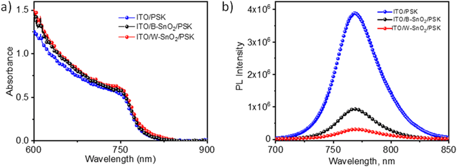 | ||
| Fig. 4 (a) UV-Vis spectra of MAPbI3 perovskite films on ITO, ITO/B–SnO2 and ITO/W–SnO2. (b) Steady-state photoluminescence spectra the same films. | ||
To investigate the functionality of both W–SnO2 and B–SnO2 as an ETL layer, perovskite solar cells were fabricated with standard methods. A schematic representation of the solar cell architecture is shown in Fig. 5a, where SnO2 layer was made by slot-die coating, while the other layers were prepared by spin coating using standard methods (see details in the experimental section). The perovskite material used was MAPbI3, prepared using a one-step method with antisolvent treatment. The current density–voltage (J–V) characteristics of champion devices, recorded under 100 mW cm−2 illumination are shown in Fig. 5b and the corresponding solar cell parameters are summarized in Table 2.
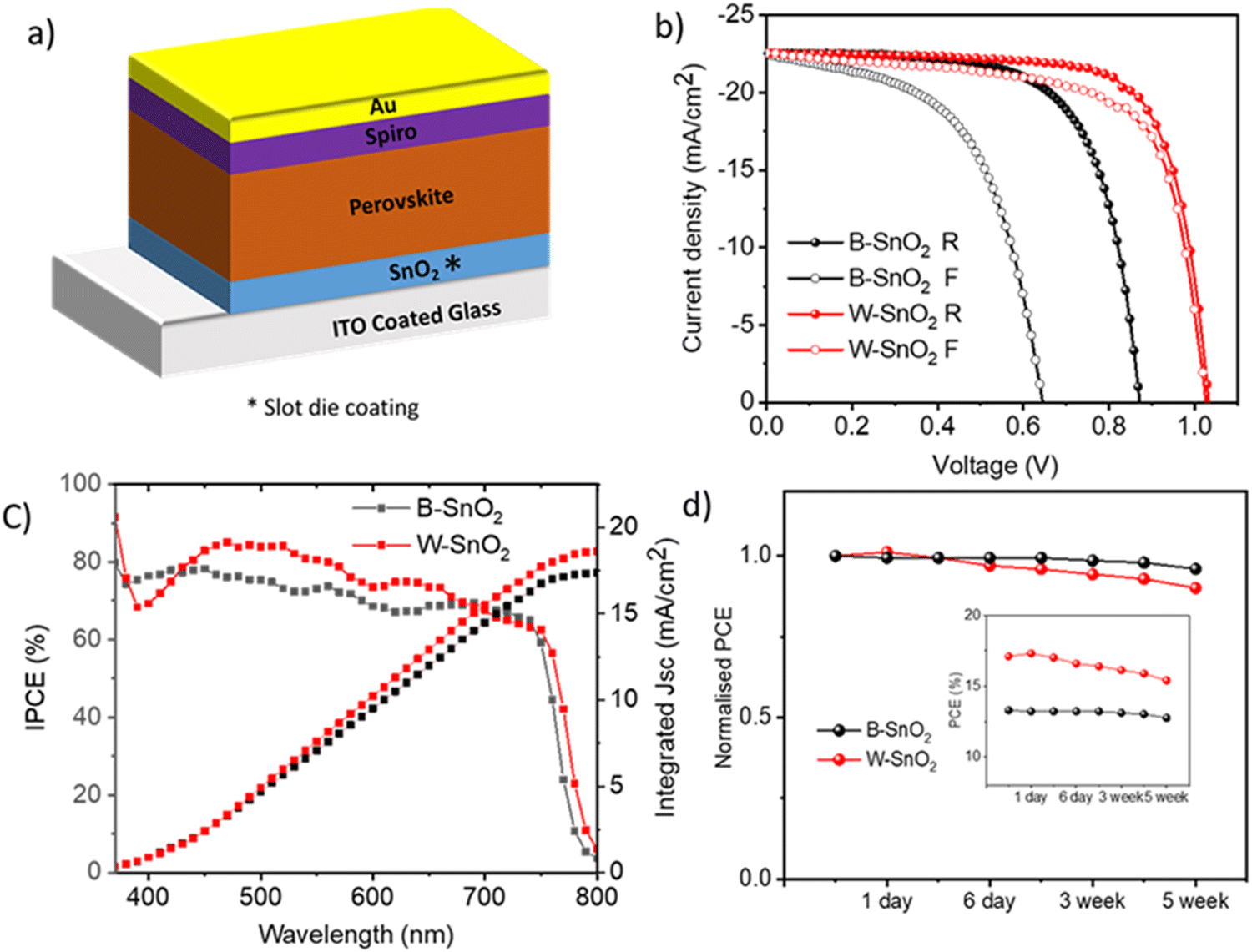 | ||
| Fig. 5 (a) N–i–p solar cell architecture; (b) champion JV curves for devices with slot-die coated SnO2 as electron transport layers; (c) IPCE spectra (d) normalized storage stability (inset actual stability over several weeks). | ||
| V OC (V) | J SC (mA cm−2) | FF (%) | PCE (%) | Hysterisis index | |
|---|---|---|---|---|---|
| W–SnO2 R | 1.03 | −22.5 | 73.6 | 17.1 | 0.07 |
| W–SnO2 F | 1.03 | −22.5 | 69.0 | 15.9 | |
| B–SnO2 R | 0.872 | −22.5 | 67.5 | 13.3 | 0.37 |
| B–SnO2 F | 0.645 | −22.4 | 55.2 | 8.0 |
We systematically varied the pump rate of the colloidal SnO2 solutions while keeping all other parameters constant. The pump rate was varied from 50 μl min−1 to 300 μl min−1 for W–SnO2 and 100 μl min−1 to 300 μl min−1 for B–SnO2. The obtained film's quality of W–SnO2 drastically changes when a low pump rate is adapted, as is evident from their solar cell performance (Fig. S5, ESI†). Higher pump rate forces more fluid to reach the substrate, which leads to an uncontrolled flow of solution on the substrate resulted in an uneven film morphology with higher thickness. Decreasing the pump rate, to find an optimum balance between pump rate and coating speed resulted in a much more uniform film. The highest power conversion efficiency of W-SnO2 based solar cell is 17.1% with a low hysteresis index of 0.07, whereas B–SnO2 showed a maximum efficiency of 13.3% with a high hysteresis index of 0.37. The hysteresis index is defined here as follows: HI = 1 − PCE(forward)/PCE(reverse). Hysteresis in PSC is generally attributed to ion movements in perovskite films and accumulations of ions at interfaces. We attribute the strong hysteresis for PSC with B–SnO2 to a poor SnO2/perovskite interface, which may be related to the ligands on the SnO2 nanoparticle or the porosity of the film.
We found a significance difference in photovoltaic performance for the two different SnO2 ETL in perovskite solar cells, see the device statistics in ESI.† (ESI† Fig. S6). There is a remarkable difference in the open circuit potential (VOC), which is about 100–200 mV larger for W–SnO2 devices. The most likely reason for this is that B–SnO2 films are poorly hole blocking, because of porosity or pin-holes, as will be shown below in separate electrochemical experiments.
We compared the incident photon to current conversion efficiency (IPCE) of the devices, in which W–SnO2 showed a maximum value of 85%, whereas B–SnO2 showed 78% in the wavelength 400–600 nm as shown in Fig. 5c. The integrated current density of W–SnO2 (18.6 mA cm−2) and B–SnO2 (17.6 mA cm−2) obtained from IPCE are lower when compared with the JV measurements, likely caused by the very low light intensity of monochromatic light used in the IPCE measurements, which give rise to photocurrents in the order of microamperes. This measurement is therefore sensitive to even small shunting effects in the devices.
The shelf life stability of the both types of cells were investigated over several weeks, see Fig. 5d. PCE of B–SnO2 remained quite stable while the efficiency of W–SnO2 started dropping to 80% of the initial value in 5 weeks.
To study the recombination mechanism in these solar cells, JSC and VOC at different intensities 10 to 100 mW cm2 were measured. Fig. 6a shows the JSC, which is approximately linearly connected to the different light intensity and the slope of doubly logarithmic plot is 0.963 and 0.957 for W–SnO2 and B–SnO2 respectively. From Fig. 6b, the VOCvs. light intensity studies showed an ideality factor of 1.92 (W–SnO2) and 2.68 (B–SnO2) for the corresponding solar cells.
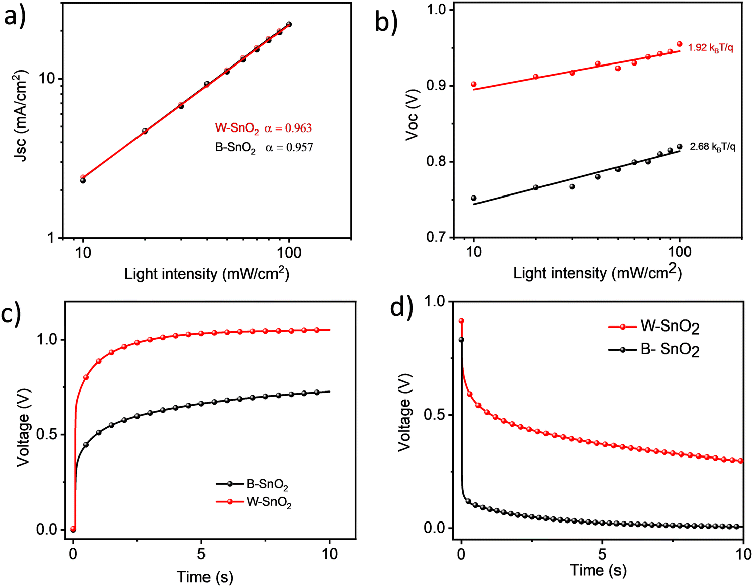 | ||
| Fig. 6 (a) JSCvs. light intensity; (b) VOCvs. light intensity; (c) VOC rise upon switching on light (1 sun); (d) VOC decay. | ||
A marked difference is also found in the VOC transients. Upon switching on the light (1 sun) it takes more than 10 s to achieve a stable VOC value. Notably, B–SnO2 devices where significantly slower than W–SnO2 (Fig. 6c). After switching off the light, part of the VOC decays rapidly in the ms-regime, while another part decay very slowly in the second-regime (Fig. 6d). The slow response of VOC to light changes is correlated to ionic motion to and from the charge-selective contacts upon charging/discharging the device. Specifically, we believe that a build-up of ions at the perovskite/SnO2 interface is important to reach the high voltages in PSC with SnO2 contacts. Clearly, it will then have a significant effect whether or not there are ligands present at the SnO2 surface, as is the case for SnO2-B.
To find out the reason for the difference in the solar cell performance for the two types of SnO2 ETL, we carried out further fundamental studies. Dynamic light scattering was used to analyze the colloidal SnO2 solutions (Fig. 7a) A significant difference in SnO2 particle size was found. The average particle size of W–SnO2 is 4–7 nm, whereas B–SnO2 shows 20–30 nm size, which is significantly larger than the reported size of 7 nm. Partially this may be ascribed to the organic ligands, but also some aggregation must be considered. Both aspects could lead to relatively porous SnO2 films upon deposition.
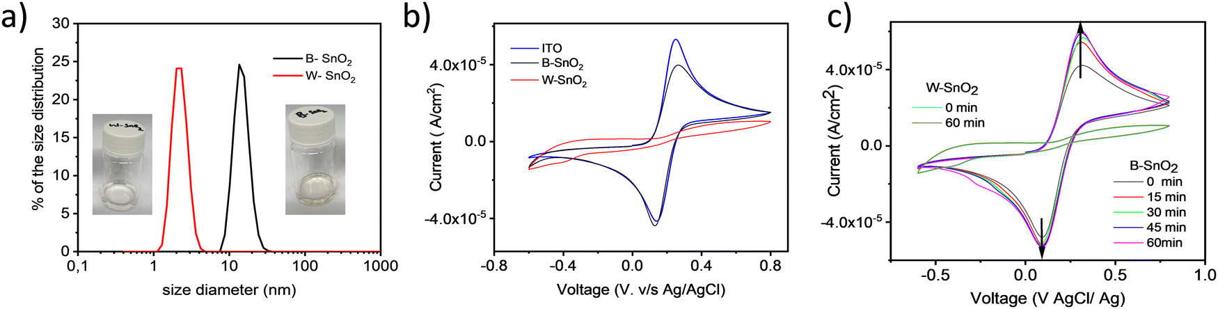 | ||
| Fig. 7 (a) Dynamic light scattering of SnO2 particles (b) cyclic voltammograms of different SnO2 films on ITO in comparison with bare ITO (c) cyclic voltammogram of SnO2 films at different time intervals. | ||
To measure the blocking behavior of both types of slot-die coated SnO2 films we carried out cyclic voltammetry (CV) by observing the anodic current density obtained with ferri/ferrocyanide redox couple. Fig. 5b shows typical cyclic voltammogram of a bare ITO (blue) in comparison with W–SnO2 (red) and B–SnO2(black). W–SnO2-coated ITO does not produce much anodic current density, confirming the film with excellent hole blocking behavior and supporting the scanning electron microscopy image of the corresponding film (Fig. 3b). In contrast, B–SnO2 exhibits higher anodic current, which indicates it is not acting as hole blocking layer in solar cell, even though it appears to completely cover the ITO surface. To confirm the coverage of both SnO2 on ITO, we also carried out x-ray photoelectron spectroscopy (see ESI† Fig. S6), we could not find any Indium peak on the XPS spectra, which indicate the complete coverage of both types of SnO2 films on ITO; this result also supports the scanning electron microscopy images of both SnO2 films.
Additional time-dependent cyclic voltammetry measurements displayed that for B–SnO2 films the anodic current density values gradually increased over a time period of one hour, in contrast to W–SnO2, which did not show any change in current density. This could point to film instability and removal of B–SnO2 particles over time. We noted a small scratch or a soft touch is enough to remove B–SnO2 films from the substrate, this we confirmed by analyzing the XPS spectra before and after a mild touch on the film (see ESI† Fig. S7), whereas W–SnO2 films are more rugged. This might also affect the cell performance, since there is a possibility of film dissolution or pinhole formation upon dropping the perovskite precursor in DMF: DMSO on to this substrate.
From here onwards, we will focus on improvement of the film quality and device performance of W–SnO2. From the literature it is clear that adding a small amount potassium fluoride (KF) helps to reduce the hysteresis effect and stability of the devices.37 We added different amount of KF (3 mg to 8 mg) into corresponding stock solution to find out the optimum amount. 6 mg/1 ml SnO2 solution was found to be the best one (see ESI† Fig. S8 and Table S1) and showed maximum efficiency of 17.5% with negligible or even no hysteresis effect. The KF-doped SnO2 has enhanced electron mobility and deep conduction band. F− ion presented in the SnO2, can migrate in to perovskite film can reduce the non-radiative recombination and trap density. Fig. 8a shows the best J–V curve and corresponding incident photon to current conversion efficiency is showed in Fig. 8b.
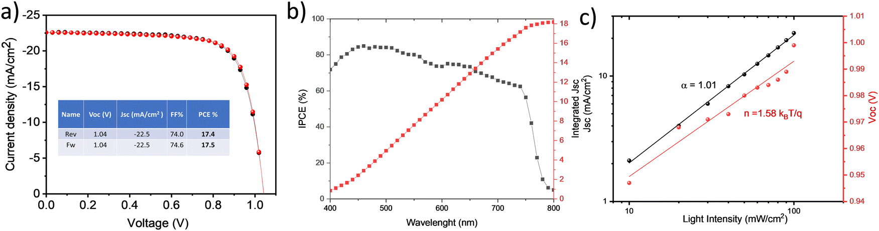 | ||
| Fig. 8 (a) Champion JV curve of W–SnO2 with KF (b) IPCE spectra of the best cell (c) Jsc and VOCvs. light intensity curve. | ||
J SC and VOC at different intensities 10 to 100 mW cm2 were also measured (Fig. 8c), the observation is in good agreement with previous results. The statistical distribution of solar cell parameters is shown in ESI† Fig. S10. The electronic structure of B–SnO2, W–SnO2 and WKF-SnO2 was studied by ultraviolet photoelectron spectroscopy (UPS) measurements and optical bandgap. Fig. S11 (ESI†) represents the valence band energy (EVB) region (left) and secondary electron cut off region (Ecutoff) region (right). The work function can be derived by subtracting the Ecutoff from standard He I irradiation energy 21.22 eV. Valence band maxima is calculated by VBM = 21.22 − (Ecutoff − EVB). The conduction band maximum (CBM) can be calculated from VBM and optical bandgap (Eg). Eg of each SnO2 was estimated from Tauc plot based on UV-vis spectroscopy (see Fig. S12, ESI†). We have summarized all the results in Table S2 in the ESI.† The energy band alignment of two different SnO2 and KF modified SnO2 are depicted in Fig. S13 (ESI†). The results indicate CBM of WKF-SnO2 more favorable for an efficient charge extraction from perovskite.
Electrochemical impedance spectroscopy measurements were also performed to analyze the charge carrier recombination in the devices, corresponding Nyquist plots was investigated at applied voltage 0.80 V under dark in the frequency range from 1000 kHz to 0.1 Hz. The equivalent circuit and fitted parameters are shown in Fig. S14 (ESI†). It is found that WKF- SnO2 shows much higher recombination resistance compared to W–SnO2 indicating that the recombination was effectively suppressed in these devices.
Conclusion
We successfully demonstrated thin film coating of two different commercially available SnO2 by slot die coating. We systematically investigated the film quality by different parameters such as pump rate, coating speed and temperature. Although film formation ability and quality of B–SnO2 found to be good when compared to W–SnO2 even though the solar cell performance was not as expected. From cyclic voltammetry measurements it appears the B–SnO2 layers are porous and do not serve well in its role as a blocking layer in the perovskite solar cell. To improve the film quality of W–SnO2, KF doping was introduced, which decreased the non-radiative recombination and lowered trap density in the solar cell.Conflicts of interest
There are no conflicts to declare.Acknowledgements
We thank the Swedish Foundation for Strategic Research (Project No. RMA15-0130) and the Standup for Energy program for financial support.References
- J. Y. Kim, J.-W. Lee, H. S. Jung, H. Shin and N.-G. Park, Chem. Rev., 2020, 120, 7867–7918 CrossRef CAS PubMed.
- C. Wehrenfennig, G. E. Eperon, M. B. Johnston, H. J. Snaith and L. M. Herz, Adv. Mater., 2014, 26, 1584–1589 CrossRef CAS PubMed.
- A. Kojima, K. Teshima, Y. Shirai and T. Miyasaka, J. Am. Chem. Soc., 2009, 131, 6050–6051 CrossRef CAS PubMed.
- J.-H. Im, C.-R. Lee, J.-W. Lee, S.-W. Park and N.-G. Park, Nanoscale, 2011, 3, 4088–4093 RSC.
- National Renewable Energy Laboratory (NREL) Best Research-Cell Efficiency Chart, Available from https://www.nrel.gov/pv/cell-efficiency.html.
- L. Chu, S. Zhai, W. Ahmad, J. Zhang, Y. Zang, W. Yan and Y. Li, Nano Res. Energy, 2022, 1, e9120024 CrossRef.
- Y. Tu, J. Ye, G. Yang, Y. Zang, L. Zhang, Y. Wang, G. Li, L. Chu and W. Yan, J. Alloys Compd., 2023, 942, 169104 CrossRef CAS.
- S. Y. Park and K. Zhu, Adv. Mater., 2022, 34, 2110438 CrossRef CAS PubMed.
- U. Bach, D. Lupo, P. Comte, J. E. Moser, F. Weissörtel, J. Salbeck, H. Spreitzer and M. Grätzel, Nature, 1998, 395, 583–585 CrossRef CAS.
- V. E. Madhavan, I. Zimmermann, C. Roldán-Carmona, G. Grancini, M. Buffiere, A. Belaidi and M. K. Nazeeruddin, ACS Energy Lett., 2016, 1, 1112–1117 CrossRef CAS.
- H.-S. Kim, C.-R. Lee, J.-H. Im, K.-B. Lee, T. Moehl, A. Marchioro, S.-J. Moon, R. Humphry-Baker, J.-H. Yum, J. E. Moser, M. Grätzel and N.-G. Park, Sci. Rep., 2012, 2, 591 CrossRef PubMed.
- T. Leijtens, G. E. Eperon, S. Pathak, A. Abate, M. M. Lee and H. J. Snaith, Nat. Commun., 2013, 4, 2885 CrossRef PubMed.
- J. You, L. Meng, T.-B. Song, T.-F. Guo, Y. (Michael) Yang, W.-H. Chang, Z. Hong, H. Chen, H. Zhou, Q. Chen, Y. Liu, N. De Marco and Y. Yang, Nat. Nanotechnol., 2016, 11, 75–81 CrossRef CAS PubMed.
- D. Liu and T. L. Kelly, Nat. Photonics, 2014, 8, 133–138 CrossRef CAS.
- S. S. Mali, C. Su Shim and C. Kook Hong, Sci. Rep., 2015, 5, 11424 CrossRef PubMed.
- S. S. Shin, W. S. Yang, J. H. Noh, J. H. Suk, N. J. Jeon, J. H. Park, J. S. Kim, W. M. Seong and S. I. Seok, Nat. Commun., 2015, 6, 7410 CrossRef CAS PubMed.
- S. S. Shin, E. J. Yeom, W. S. Yang, S. Hur, M. G. Kim, J. Im, J. Seo, J. H. Noh and S. I. Seok, Science, 2017, 356, 167–171 CrossRef CAS PubMed.
- Q. Jiang, X. Zhang and J. You, Small, 2018, 14, 1801154 CrossRef PubMed.
- C. Altinkaya, E. Aydin, E. Ugur, F. H. Isikgor, A. S. Subbiah, M. De Bastiani, J. Liu, A. Babayigit, T. G. Allen, F. Laquai, A. Yildiz and S. De Wolf, Adv. Mater., 2021, 33, 2005504 CrossRef CAS PubMed.
- P. Wu, S. Wang, X. Li and F. Zhang, J. Mater. Chem. A, 2021, 9, 19554–19588 RSC.
- S. Thampy, B. Zhang, K.-H. Hong, K. Cho and J. W. P. Hsu, ACS Energy Lett., 2020, 5, 1147–1152 CrossRef CAS.
- W. Ke, G. Fang, Q. Liu, L. Xiong, P. Qin, H. Tao, J. Wang, H. Lei, B. Li, J. Wan, G. Yang and Y. Yan, J. Am. Chem. Soc., 2015, 137, 6730–6733 CrossRef CAS PubMed.
- Q. Jiang, Y. Zhao, X. Zhang, X. Yang, Y. Chen, Z. Chu, Q. Ye, X. Li, Z. Yin and J. You, Nat. Photonics, 2019, 13, 460–466 CrossRef CAS.
- Q. Jiang, L. Zhang, H. Wang, X. Yang, J. Meng, H. Liu, Z. Yin, J. Wu, X. Zhang and J. You, Nat. Energy, 2016, 2, 16177 CrossRef.
- Z. Xiong, X. Chen, B. Zhang, G. O. Odunmbaku, Z. Ou, B. Guo, K. Yang, Z. Kan, S. Lu, S. Chen, N. A. N. Ouedraogo, Y. Cho, C. Yang, J. Chen and K. Sun, Adv. Mater., 2022, 34, 2106118 CrossRef CAS PubMed.
- L. Vesce, M. Stefanelli, F. Rossi, L. A. Castriotta, R. Basosi, M. L. Parisi, A. Sinicropi and A. Di Carlo, Prog. Photovoltaics Res. Appl., 2024, 32, 115–129 CrossRef CAS.
- Y. Galagan, F. Di Giacomo, H. Gorter, G. Kirchner, I. de Vries, R. Andriessen and P. Groen, Adv. Energy Mater., 2018, 8, 1801935 CrossRef.
- J. A. Smith, O. S. Game, J. E. Bishop, E. L. K. Spooner, R. C. Kilbride, C. Greenland, R. Jayaprakash, T. I. Alanazi, E. J. Cassella, A. Tejada, G. Chistiakova, M. Wong-Stringer, T. J. Routledge, A. J. Parnell, D. B. Hammond and D. G. Lidzey, ACS Appl. Energy Mater., 2020, 3, 5552–5562 CrossRef CAS PubMed.
- T. Bu, J. Li, F. Zheng, W. Chen, X. Wen, Z. Ku, Y. Peng, J. Zhong, Y.-B. Cheng and F. Huang, Nat. Commun., 2018, 9, 4609 CrossRef PubMed.
- D. Richards, D. Burkitt, R. Patidar, D. Beynon and T. Watson, Mater. Adv., 2022, 3, 8588–8596 RSC.
- B. Taheri, F. De Rossi, G. Lucarelli, L. A. Castriotta, A. Di Carlo, T. M. Brown and F. Brunetti, ACS Appl. Energy Mater., 2021, 4, 4507–4518 CrossRef CAS PubMed.
- D.-K. Lee, D.-N. Jeong, T. K. Ahn and N.-G. Park, ACS Energy Lett., 2019, 4, 2393–2401 CrossRef CAS.
- B. Taheri, E. Calabrò, F. Matteocci, D. Di Girolamo, G. Cardone, A. Liscio, A. Di Carlo and F. Brunetti, Energy Technol., 2020, 8, 1901284 CrossRef CAS.
- J. B. Whitaker, D. H. Kim, B. W. Larson, F. Zhang, J. J. Berry, M. F. A. M. van Hest and K. Zhu, Sustainable Energy Fuels, 2018, 2, 2442–2449 RSC.
- Y. Hu, S. Si, A. Mei, Y. Rong, H. Liu, X. Li and H. Han, Sol. RRL, 2017, 1, 1600019 CrossRef.
- G. S. Han, J. Kim, S. Bae, S. Han, Y. J. Kim, O. Y. Gong, P. Lee, M. J. Ko and H. S. Jung, ACS Energy Lett., 2019, 4, 1845–1851 CrossRef CAS.
- S. Zhang, H. Gu, S.-C. Chen and Q. Zheng, J. Mater. Chem. C, 2021, 9, 4240–4247 RSC.
Footnote |
| † Electronic supplementary information (ESI) available. See DOI: https://doi.org/10.1039/d4ma00351a |
| This journal is © The Royal Society of Chemistry 2024 |