
 Open Access Article
 This Open Access Article is licensed under a Creative Commons Attribution-Non Commercial 3.0 Unported Licence
Investigation of different degradation pathways for organic photovoltaics at different temperatures†
Bradley P.
Kirk
 a,
Amira R.
Alghamdi
ab,
Matthew J.
Griffith
cd,
Xun
Pan
a,
Martyn
Jevric
a,
David A.
Lewis
a,
Gunther G.
Andersson
a and
Mats R.
Andersson
*a
a,
Amira R.
Alghamdi
ab,
Matthew J.
Griffith
cd,
Xun
Pan
a,
Martyn
Jevric
a,
David A.
Lewis
a,
Gunther G.
Andersson
a and
Mats R.
Andersson
*a
aFlinders Institute for Nanoscale Science and Technology, College of Science and Engineering, Flinders University, P.O. Box 2100, Adelaide, SA 5001, Australia. E-mail: mats.andersson@flinders.edu.au
bDepartment of Physics, College of Science, Imam Abdulrahman Bin Faisal University, P.O. Box 1982, Dammam 31441, Saudi Arabia
cFuture Industries Institute, University of South Australia, Mawson Lakes, SA 5095, Australia
dSchool of Aerospace, Mechanical and Mechatronic Engineering, University of Sydney, Camperdown, NSW 2006, Australia
First published on 18th April 2024
Abstract
The lifetime of organic photovoltaics (OPVs) is a significant challenge for the technology to become commercially viable. Mechanisms of thermally induced degradation are extremely complex due to the nature of the materials and structures in OPVs, each with varying responses to thermal cycling. To date, approaches have focused on small-scale devices, with a limited number of studies focusing on cells made by scalable methods, leaving the stability of materials for large scale devices a substantial unsolved challenge. Ageing OPVs at elevated temperatures is normally performed to reduce experimental times but care must be taken to not introduce new degradation pathways which are not relevant for actual operational conditions. In this paper, we have investigated the thermal degradation of active layer blend of PPDT2FBT:PC61BM that has been deposited via slot-die coating. By combining surface and thin-film characterisation techniques with dynamic mechanical thermal analysis (DMTA), we have investigated the thermal behaviour of the blend, and how it changes upon annealing at two elevated temperatures; 85 °C, and 120 °C. Our results show that at 120 °C large crystals made of PC61BM are formed already after 8 h while at 85 °C large crystals did not form even after 6 months annealing. The fullerene crystallisation at 120 °C plays a significant role in fast thermal degradation of the solar cells, whereas at 85 °C the change in thermal behaviour is dominated by small morphological changes that affect changes in OPV performance. These results clearly shows that care must be taken when performing accelerated ageing of OPV materials.
1. Introduction
With the push towards cost-effective, renewable energy sources, there has been an increased interest in the development of highly functional organic photovoltaics (OPVs). The potential is owed to their ability to fabricate these thin, lightweight, and flexible devices using scalable, low cost roll-to-roll coating/printing methods resulting in lower manufacturing costs when compared to conventional silicon solar panels.1–3 In the past decade, there has been significant improvements of device performance for OPV technology, leading to power conversion efficiencies (PCEs) exceeding 19% for small-scale single junction devices,4,5 while large-area OPV modules (>100 cm2) have reached above 12%.6 There has also been an interest in the development of OPVs for indoor applications due to their ability to work effectively under low-light and artificial lighting conditions.7–9Although performance and fabrication cost are important aspects for the development of OPVs, device lifetime/stability is equally important, yet has seen less research focus10 and needs to be improved.11 In terms of stability, there are five major factors that can negatively impact the device performances during normal operation of OPVs: thermal cycling due to environmental conditions,12,13 exposure to oxygen, moisture,14,15 UV radiation,16,17 and mechanical18–20 degradation. These factors typically combine to produce two significant decay trends in the device performance: an initial drop in efficiency referred to as the “burn-in loss”, followed by a longer term sustained linear degradation in the efficiency.21–23
Continuous illumination from a light source can result in an increase of the working temperature, especially when operating in outdoor conditions with direct sun-exposure, which is relevant for the thermal stability. As the majority of OPVs contain a bulk-heterojunction (BHJ) structured active layer where a donor and an acceptor material are intermixed at the nanometre scale, there is a substantial risk that the thermal energy increases the mobility of these active materials, resulting in a change in morphology of the active layer, especially when the temperature exceeds the glass transition temperatures of the active layer blend.24,25 This elevated temperature may also lead to degradation via the material diffusion at the interface of electrodes and transport/extraction/interface layers.26–28
To date, it has been agreed that 65–85 °C range is the typical maximum temperature experienced by OPVs in their operational environments, known as the high temperature dark storage condition, and recognised as a global standard by the International Summit on OPV Stability (ISOS) consensus test community.29 As such, a few reports have examined the degradation of OPVs at this high temperature ageing condition. This includes Chaturvedi et al. who investigated the degradation of different device configurations of PTB7-Th:IEICO-4F devices for an period of 750 h (31 days),30 while Wu et al. used 85 °C for 4000 minutes (2.7 days) to demonstrate their improved thermal stability using a newly synthesised donor polymer, PMZ2, when compared with PM6.31
The problem associated with testing devices at this ageing temperature, especially for more thermally robust devices, is that long periods of, sometimes surpassing 1 year, are required for a significant amount of degradation to occur.32,33 This length of time to generate data can result in difficulties comparing materials and strategies for improving device lifespan, slowing the rate of research. In order to shorten these experiments, higher temperatures (>85 °C) are often employed to accelerate degradation mechanisms in OPV devices, reducing degradation test time to less than a month.12,13,34 A wide range of elevated temperatures have been used to accelerate degradation, including 80 °C,35–37 85 °C,27,28,30,38–43 90 °C,44 100 °C,13,34,45 110 °C,46 120 °C,47,48 130 °C,49 140 °C,50 150 °C,51–53 160 °C,44 180 °C,12 and even up to 200 °C.44
An issue that arises from using elevated temperatures for ageing studies is the potential of additional degradation pathways that only occur at elevated temperatures, well above normal operating temperature of the OPV. For example, He et al. had observed that for an inverted OPV configuration, heating to 200 °C caused silver penetrating into the active layer, resulting in a reduction of device performance, which was not observed at lower temperatures.44 Jang et al. also observed that when comparing devices fabricated using PTB7:PC71BM either, heating at 80 °C for 10 days showed minimal change in performance, while exposure at 140 °C resulted in significant burn-in degradation for the devices fabricated using a single deposition of the active layer, while sequential deposition of the active layer devices were not affected.54 Xu et al. have heated devices at a range of ageing temperatures, and found that PBTTT-EFT:PC71BM started to degrade significantly above 80 °C, whereas for a PBTTT-EFT:PC71BM blend, performance started to degrade at 100 °C.47
One promising active layer material blend for scalable OPV fabrication is poly[(2,5-bis(2hexyldecyloxy)phenylene)-alt-(5,6-difluoro-4,7-di(thiophen-2-yl)benzo[c][1,2,5]thiadiazole)]:[6,6]-phenyl-C61-butyric acid ester (PPDT2FBT:PC61BM) (structures seen in Fig. 1a). This blend can be successfully deposited using slot-die coating.55 When incorporating PPDT2FBT with PC61BM, spin-coated devices achieved a PCE of 9.1%.56 PPDT2FBT:PC61BM has also been demonstrated to enable slot-die coated devices at a variety of scales with minimal performance loss.8,48,55,57 Although PPDT2FBT:PC71BM OPVs are able to achieve higher performances,58 PC71BM is significantly more expensive compared to PC61BM, which adds more cost for large scale printed devices.55
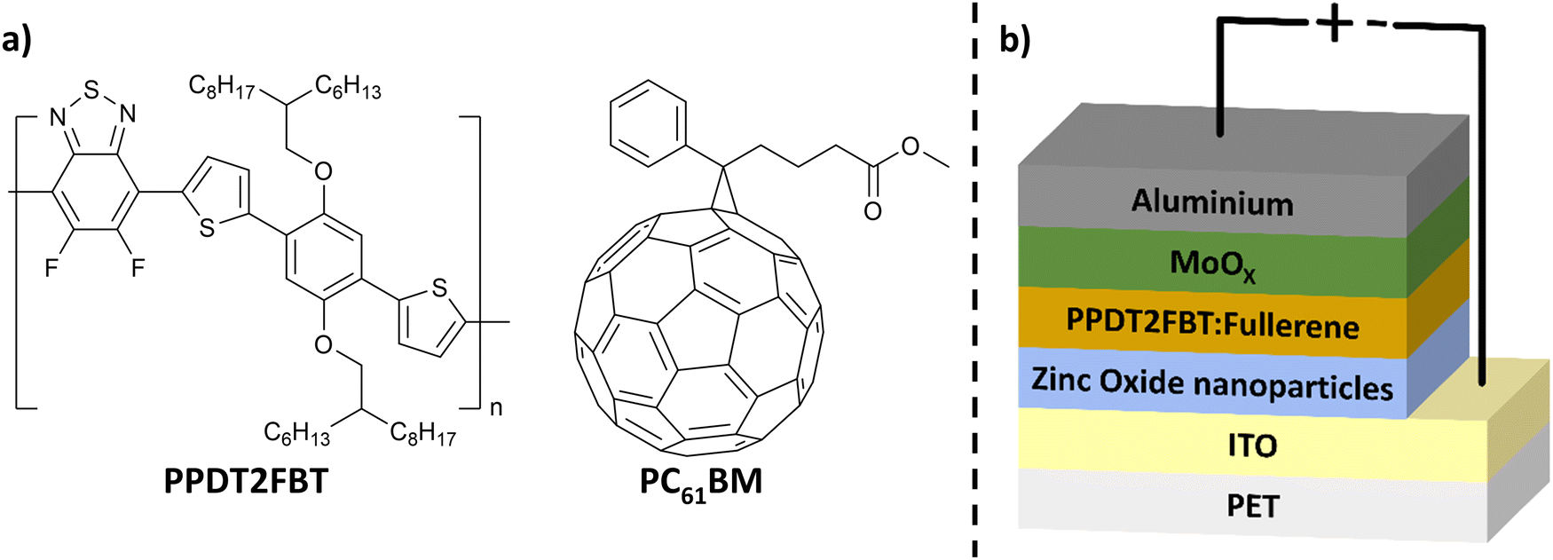 | ||
| Fig. 1 (a) Chemical structure of PPDT2FBT & PC61BM and (b) schematic illustration of inverted OPV structure used in this work. | ||
A handful of studies have been performed to investigate the stability of both slot-die and spin-coated PPDT2FBT:PC61BM devices. For lower temperature degradation (60 °C), paired with constant illumination and without humidity control, Mainville et al. observed that the PPDT2FBT:PC61BM devices lasted 220 hours (9 days) before PCE dropped below 80% of the initial PCE.57 PPDT2FBT:PCBM devices have also been tested at higher degradation temperatures (120–130 °C),48,55,59 with one paper demonstrating PPDT2FBT:PC61BM devices to be stable at 130 °C for 220 h.57
Expanding on our previous thermal degradation study of PPDT2FBT:PC61BM,55 we investigated the major degradation pathways of PPDT2FBT:PC61BM materials at both 85 °C and 120 °C, focusing on how the morphology of the blends changed when exposed to different elevated temperatures for specific amounts of time, including up to 6 months at 85 °C. Scanning electron microscopy (SEM) and Auger electron spectroscopy (AES) techniques were used to investigate the formation of features and defects that were seen at the surface of the aged active layers. Dynamic mechanical thermal analysis (DMTA) was implemented to investigate the changes of thermal behaviour as the active layer blends were aged at different temperatures. The morphological changes were used to explain the degradation behaviour of the devices at the studied temperatures, revealing that different degradation pathways occurs at 85 °C and 120 °C for the PPDT2FBT:PC61BM blend.
2. Results and discussion
2.1. Device performance stability
As demonstrated previously, PPDT2FBT:PC61BM devices appeared to be relatively stable when thermally annealed at 85 °C for 16 days, compared to dark, room temperature ageing.55 In order to monitor a period more relevant for thermal degradation, the thermal degradation was tested for 6 months. This length of time was hypothesised to allow for a more significant performance decrease to be observed. For a comparison, some devices were also aged at 120 °C in dark under nitrogen conditions (seen in Fig. 2).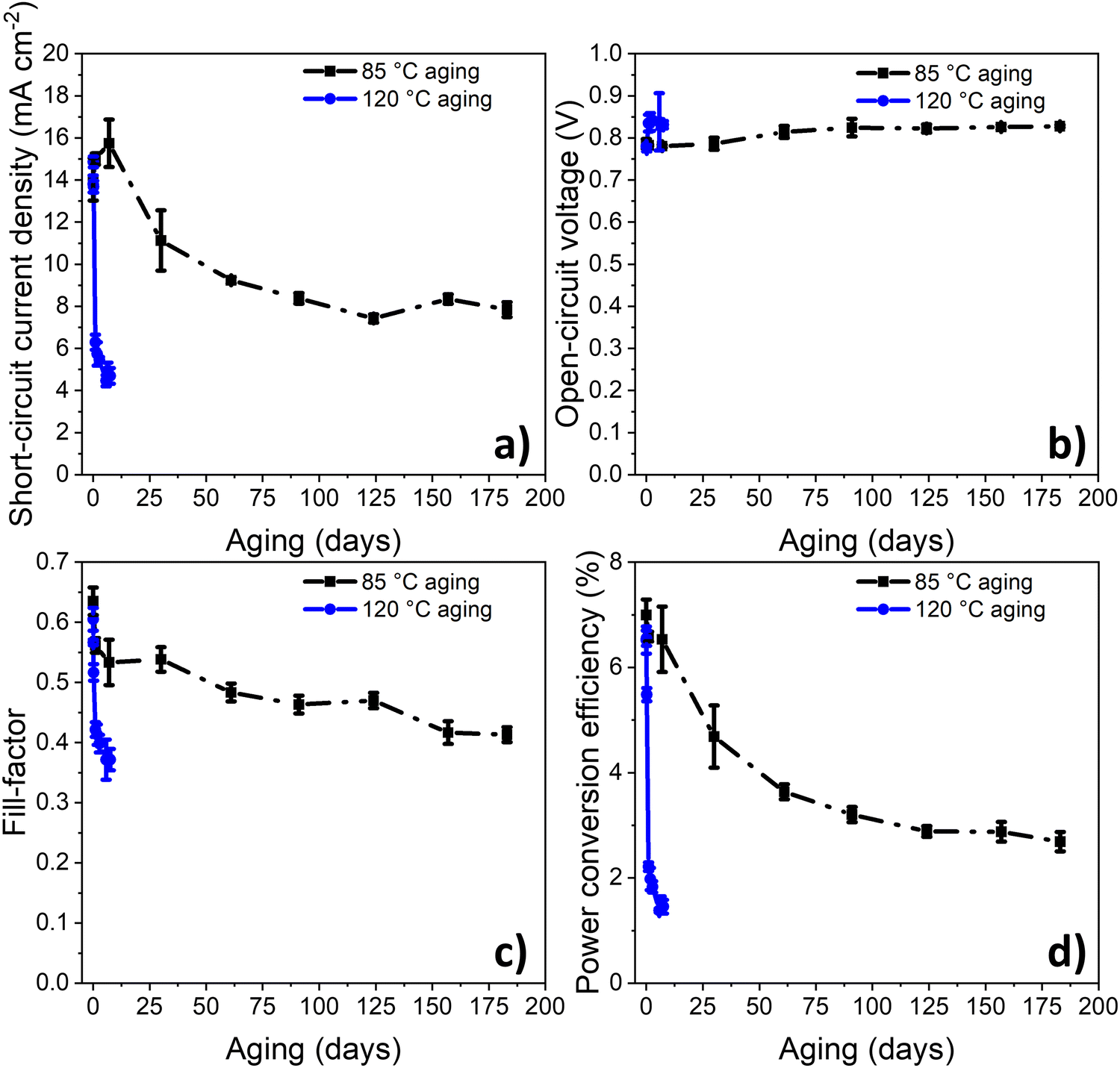 | ||
| Fig. 2 (a) Short-circuit current density (JSC), (b) open-circuit voltage (VOC), (c) fill-factor (FF) and (d) power conversion efficiency (PCE) changes as a function of ageing time for devices at 85 °C or 120 °C under dark nitrogen conditions. | ||
From the previous study,55 the PCE degradation behaviour for 16 days at 85 °C followed a downward linear trend, indicating the lack of burn-in degradation within the 16 day timeframe. In this study, when the range of degradation study was increased to 6 months (seen in Fig. 2), the burn-in trend was more distinguishable, lasting around 120–150 days. This result reveals that the burn-in degradation takes a relatively long time to cause degradation of the PPDT2FBT:PC61BM devices at 85 °C, especially when compared to the 120 °C degradation trend.
Another interesting observation is the magnitude of burn-in degradation when comparing PPDT2FBT:PC61BM devices ageing at 85 °C or 120 °C, dropping down to 2.7% after 183 days, and 1.5% after 7 days, respectively. For JSC, both 85 °C and 120 °C aged device sets saw a decrease, although at 120 °C, JSC decrease down to 4.7 mA cm−2 after 7 days, while at 85 °C, JSC decreased down to 7.8 mA cm−2 after 183 days. The FF also followed a similar trend, with FF of 120 °C aged devices dropping down to 0.37 after 7 days, while that of 85 °C aged devices reached 0.41 after 183 days. As for the VOC, both sets of aged devices saw a small increase towards 0.84 V. In terms of the decrease in JSC and FF, it is suspected to be related to changes of the active layer morphology, with previous studies showing PC61BM crystallisation to be a likely contributor.55,60,61 The increase in VOC is likely related to the reduction of energetic disorder at the BHJ/ZnO interface, which has been observed for BTID-2F:PC71BM devices when stored under dark conditions.62
To gain additional understanding of the degradation of PCE under varying thermal ageing conditions, we used the Arrhenius-type exponential (eqn (1)). In the OPV field, Arrhenius-type exponential is for the basic prediction of device lifespan, based on the activation energy of the degradation pathway (Ea), and the ageing temperature (T) used for the degradation studies, as well as the reaction dependant constant (A) and the gas constant (R = 8.314 kJ mol−1 K−1).29
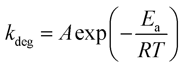 | (1) |
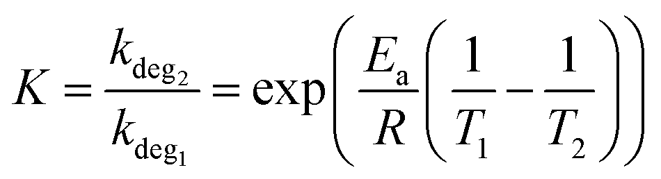 | (2) |
The decay rate from eqn (1) can also be used to investigate the acceleration factor (K) between two ageing temperatures (T1 & T2) (eqn (2)). It is worth noting that this decay method is predominately used in chemical-based degradation (including photo-oxidation),63–65 however, it has been demonstrated to show the change in degradation rate under accelerated thermal again conditions.66,67 The decay model also assumes the kdeg is constant when ageing temperature is constant and Ea is constant when varying the degradation temperature.68
To determine the decay rate at 85 °C and 120 °C, an exponential decay fit (eqn (S1), ESI†) was computationally fitted to the experimental data (Fig. S1 and S2, ESI†), resulting in values of 0.02 day−1 and 1.17 day−1, respectively. Using the determined activation energy of thermal degradation of OPVs (under light soaking), 90 kJ mol−1,68 it is expected, from applying eqn (2), that a temperature increased from 85 °C (358 K) to 120 °C (393 K) would result in an acceleration factor of 15. Whereas from the experimental results, it was found that the acceleration factor was 50. This large disparity in the acceleration factor values indicates that different degradation pathways (with different Ea) dominate at the two studied temperatures.
2.2. Charge carrier dynamics of thermally aged OPVs
To understand the changes in dynamic charge carrier generation, transport, and recombination processes in the annealed OPV devices, the charge carrier mobility was studied using photoCELIV, the carrier lifetime was extracted using transient photovoltage (TPV) measurements and the photogenerated carrier density was determined using time-resolved charge extraction (TRCE). The photoCELIV measurements enable the carrier mobility to be determined from the peak time of the current transient (tmax), the maximum value of the photocurrent transient and the capacitive current baseline value as reported in the literature.69 The transient carrier lifetime was determined by fitting a single exponential decay to the transient photovoltage curves measured using the TPV technique and then converted to a carrier lifetime of the entire photogenerated population from consideration of the rate law kinetics as reported in previous literature.70 The charge carrier density present at the same intensity lifetime values were determined was calculated by integrating the current transient obtained from the TRCE technique. Devices for these studies were measured after an ageing treatment for a 7-day time period, either at 85 °C or 120 °C.As revealed in the photoCELIV curves in Fig. 3a, the thermal ageing of the PPDT2FBT:PC61BM devices has strong influence over the transport processes in the devices. A systematic decrease in tmax was coupled with systematic decrease in the observed photogenerated charges as the ageing temperature was increased from room temperature to 85 °C and then again to 120 °C. These trends result in a clear increase in the charge carrier mobility as the ageing temperature of devices is increased (Fig. 3c). When averaging the charge mobility values obtained between 0.3–1 Sun light intensity, it was determined that devices annealed at room temperature, 85 °C and 120 °C had carrier mobility values of (8.5 ± 0.6) X 10−5 cm2 V−1 s−1, (9.9 ± 0.9) X 10−5 cm2 V−1 s−1 and (12.5 ± 1.8) X 10−5 cm2 V−1 s−1, respectively. This increase in mobility upon thermal ageing is likely related to increased phase purity/crystallisation of PC61BM, allowing for more effective movement of free charge out of the active layer. Crystallisation has been observed in previous literature with P3HT:PC61BM devices, where it was found that increasing the annealing temperature resulted in an increase in carrier mobility.71 When it comes to influencing the P3HT:PCBM OPV device performance, it is suspected that the improvement in mobility occurs due to the crystallisation of the P3HT polymer72,73 or the PC61BM.71 It is also noted that the capacitive current dropped once the device were subjected to a thermally elevated ageing (either 85 °C or 120 °C), indicative of a removal of dark doping density in the active layer with thermal ageing.
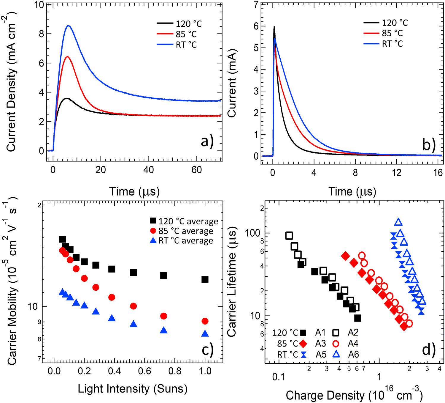 | ||
| Fig. 3 Charge Carrier Dynamics of PPDT2FBT:PC61BM devices that have either been aged at room temperature, 85 °C or 120 °C for 7 days. Figures include (a) photoCELIV curves obtained at ∼1 Sun, (b) current transients obtained from the TRCE technique, (c) charge carrier mobility obtained via photoCELIV measurements as a function of light intensity, and (d) carrier lifetime in as a function of charge density. | ||
The current transients from charge extraction measurements, shown in Fig. 3b, confirm that thermal ageing of the PPDT2FBT:PC61BM devices has a strong influence on the photogenerated charge in the devices. There are clear changes in the transient current pulse shape for the devices aged at 85 °C and 120 °C, with the increase in ageing temperature resulting in a decrease in area under the pulse, indicating a reduced amount of charge generation in these devices at equivalent light illumination levels. When the carrier lifetime values determined from TPV measurements are plotted against the photogenerated charge values determined from the TRCE measurements (Fig. 3d), a significant decrease in the carrier lifetime is observed at equal charge densities as the annealing temperature of the devices is increased to 85 °C, with a further significant decrease observed upon increasing the ageing temperature to 120 °C. Since the mobility of carriers was earlier established to increase with ageing temperature, the charge extraction results from Fig. 3b suggest that the probability of either geminate, trap-assisted or bimolecular recombination in PPDT2FBT:PC61BM devices increases with ageing temperature, leading to a reduced photogenerated charge density. The carrier lifetime results from Fig. 3d probe a longer time scale, with the reduced lifetime indicating an increased bimolecular recombination rate between separated free charges in PPDT2FBT:PC61BM devices with increases in the ageing temperature. The slope of the lifetime vs charge density plots also changes after thermal ageing, suggesting a change to the density of states in the active layer material that is consistent with the reduced dark doping density observed in the photoCELIV measurements in Fig. 3a. The increased recombination at both fast (geminate) and slower (bimolecular) times scales with an increase in ageing temperature is hypothesised to originate from the phase domain sizing increasing, or the formation and growth of fullerene crystals within the BHJ. Previous work has shown that when PPDT2FBT:PC61BM was annealed at 120 °C for 8 hours, fullerene microcrystals were observable at the surface of the active layer.55 With the formation of fullerene microcrystals, as well as potential increased phase size in the polymer, there is an increased probability that the induced excitons are unable to diffuse towards the donor/acceptor interface for charge separation, leading to exciton recombination.
The charge carrier dynamics measurements revealed that the carrier mobility improved as a function of ageing temperature, however, there is also a corresponding significant increase in the recombination. Although the increase in free charge mobility is typically considered to be a positive driver for OPV device performance, the increased recombination rate counteracts these mobility improvements. For the device aged at 85 °C, the effects of these counteracting mechanisms appear to have a neutral effect on the overall device performance, and thus the PCE does not show significant reductions over a 7-day time period. For the devices aged at 120 °C the scale of the mobility enhancement is dominated by the scale of the increased recombination and the performance of the devices subsequently shows significant drops in comparison to the device aged at room temperature. The investigations of the dynamic charge carrier behaviour suggest it is likely that an increase in charge carrier recombination is a leading factor for the reduction in performance for thermally aged PPDT2FBT:PC61BM devices.
The J–V curves measured throughout the ageing process at 85 °C and 120 °C show similar trends (Fig. S3, ESI†), with the short circuit current dropping in magnitude to a much larger degree than the slope of the curve changes as it passes through short circuit and into reverse bias (where extraction is artificially accelerated due to the applied field). Examining the current extracted at −1 V compared to the current extracted at short circuit indicates a step change with respect to ageing time (as seen in Fig. S4, ESI†), where ∼20% more current is extracted in reverse bias after the 4th ageing point for each temperature (30 days for 85 °C and 1 day for 120 °C, reflecting the accelerated degradation at 120 °C). After this time point the ratio of current extracted in reverse bias compared to short circuit exhibits negligible changes for all further ageing times. The increase in the photocurrent under reverse bias around the 4th ageing point is consistent with a reduced mobility-lifetime product, which from the data in Fig. 3 could be assigned to slow (non-geminate) recombination. However, the dominant effect driving performance reductions is the large magnitude of the current reduction, which with exception of the step-change at the 4th ageing point for each temperature, drops in consistent proportions with respect to applied bias as the devices are aged. This result implies that the dominant driver of the performance reductions is a loss of free charge generation, likely due to increased geminate recombination.
2.3. Bulk heterojunction morphology investigation
To investigate the morphological changes of the active layer containing PPDT2FBT:PC61BM, half devices (PET/ITO/ZnO nanoparticles (NPs)/BHJ) were annealed at 120 °C and 85 °C in the dark under nitrogen. Although device performance degradation measurements were conducted on full devices (PET/ITO/ZnO NPs/BHJ/MoOX/Al), the half device allowed for in-depth assessment of changes to the active layer upon thermal ageing.For PPDT2FBT:PC61BM film annealed at 120 °C for 8 hours, 3-dimensional microcrystals appeared that are clearly distinguishable from the surface of the active layer as seen scanning electron microscopy (SEM) images in Fig. 4. From previous studies, with the utilization of Auger electron spectroscopy (AES), these microcrystals were likely to be PC61BM.55 The surface of the half devices was characterised by SEM after annealing at 85 °C for 1, 3 & 6 months, with the images shown in Fig. 5.
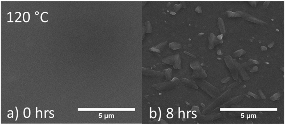 | ||
| Fig. 4 SEM images of PPDT2FBT:PC61BM BHJ surface (a) before and after (b) annealing at 120 °C for 8 hours. | ||
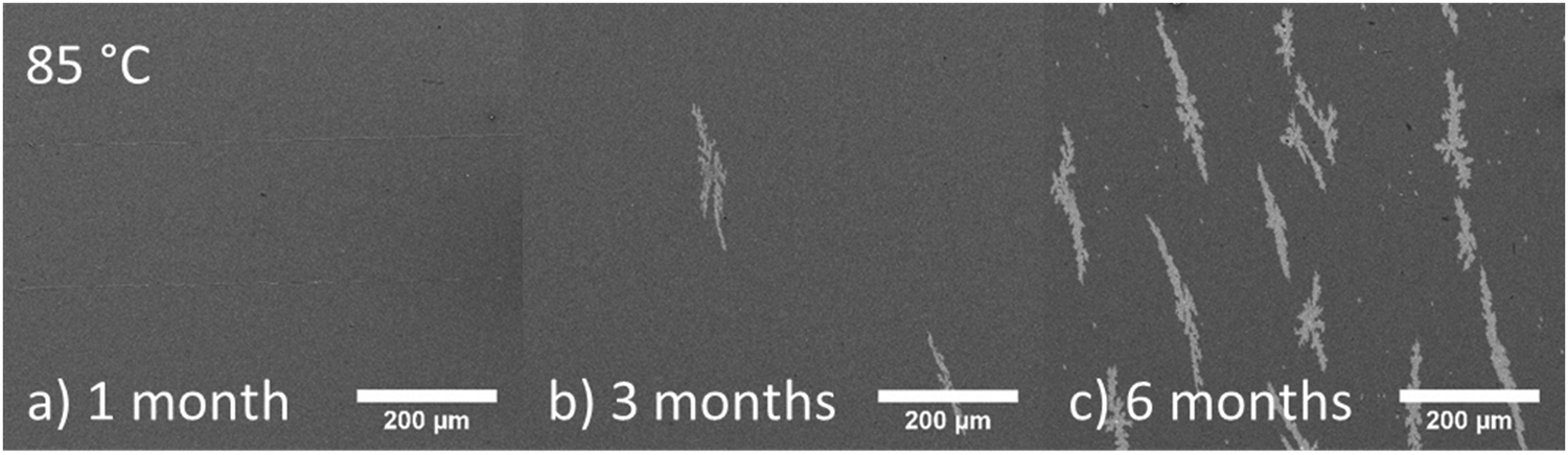 | ||
| Fig. 5 SEM images of PPDT2FBT:PC61BM BHJ surface after either annealing at 85 °C for either (a) 1 month, (b) 3 months or (c) 6 months. | ||
Before heating, the surface of the BHJ appeared relatively smooth and feature-less. After one month of annealing at 85 °C, no significant change to the active layer was observed, while the BHJ layer still remained relatively featureless. After 3 months of annealing at 85 °C, the appearance of micro-features was observed. The features are flat and long (∼200 μm length, ∼30 μm width), and share a similar orientation along the layer surface. After 6 months, the population of these features increased, yet the size remained the same. Another observation associated with the features is that they appeared to be present at the very surface of the active layer, with no noticeable shadows around the features, as in Fig. 4b. To confirm this, stylus profilometry of the features was performed to see if the height map is distinguishable from the BHJ surface (seen in Fig S8 in ESI†).
The comparison of SEM images with the profilometer map showed no significant height features that would be expected for 3D crystals growing out of the surface. The small bright spots, however, are assumed to be associated with aggregates that were present prior to thermal annealing, or potential contaminates. The question then arises, whether the flat features observed in 85 °C aged PPDT2FBT:PC61BM are composed of PC61BM, similar to the 120 °C aged active layer, or whether they have a different composition. AES and neutral impact collision ion scattering spectroscopy (NICISS) were utilised to investigate this question.
2.4. Elemental characteristics of microfeatures
The advantage of AES is its short probing depth of about 10 nm, minimising the contribution of the underlying BHJ, and electrode underneath in the resulting spectra. Based on the molecular structure of the photoactive materials present in the BHJ, carbon, sulphur, nitrogen, oxygen, and fluorine would be detectable from the presence of PPDT2FBT, while the presence of PC61BM would result in the signal from only carbon and oxygen. From the resulting AES spectra (as seen in Fig. S13 in ESI†), the presence of sulphur (152 eV), carbon (272 eV) and oxygen (508 eV) were identified, whereas nitrogen (379 eV) and fluorine (647 eV) were not noticeable. The difference in peak can be explained by two potential factors, the varying number of atoms per element, as well as the elemental sensitivity factors. When operating the AES with an electron beam energy of 10 keV, the sensitivity factors for carbon, nitrogen, oxygen, fluorine & sulphur are 0.28, 0.60, 0.79, 1.61 & 2.43, respectively.74 Firstly, due to the relatively high sensitivity factor, even a small amount of sulphur allows for a significant peak to be observed, whereas for carbon, the high amount present in both the polymer and fullerene results in a large peak.The low sensitivity factor and low atomic concentration of nitrogen and oxygen leads to the peaks being either difficult to distinguish, or unable to be resolved from the background. What is difficult to explain is, although fluorine has a high sensitivity factor, the fluorine peak is unable to be distinguished from the background of the AES spectra, even though the element is present in PPDT2FBT. As a theoretical comparison of atomic percentages of carbon and sulphur, it is expected that PPDT2FBT, containing 52 carbons & 3 sulphurs per repeating unit, would have a carbon and sulphur atomic percentage of 94.5% and 5.5% respectively, whereas PC61BM would have 100% carbon due to no sulphur being present in the molecule. As such, the change in sulphur atomic percentage can be implemented for determining the unit![[thin space (1/6-em)]](https://www.rsc.org/images/entities/char_2009.gif) :molecule ratio of polymer:fullerene at specific locations.
:molecule ratio of polymer:fullerene at specific locations.
From AES results (Table 1), the surface of the BHJ appears to have a high percentage of PPDT2FBT polymer, rather than PC61BM based on the relative atomic percentage between sulphur and carbon at the surface. The sulphur content of a thin film of pure PPDT2FBT was determined to be 3.8 ± 0.8%, while the BHJ had a percentage for 4.0 ± 0.5%. Regardless of annealing temperature, the BHJ surface (not including crystals) appears to be dominated by the polymer.
| Location | %Carbon | %Sulphur | ||
|---|---|---|---|---|
| BHJ (85 °C annealed) | 96.0 | ±0.5 | 4.0 | ±0.5 |
| BHJ (120 °C annealed) | 96.4 | ±0.2 | 3.6 | ±0.2 |
| Short crystals | 98.2 | ±0.2 | 1.8 | ±0.2 |
| Long crystals | 98.3 | ±0.2 | 1.7 | ±0.2 |
| Flat feature | 98.0 | ±0.5 | 2.0 | ±0.5 |
| PPDT2FBT | 96.2 | ±0.8 | 3.8 | ±0.8 |
When investigating the composition of the features identified as crystals, the sulphur/carbon ratio was also calculated; with a value close to 5.5% sulphur indicating the presence of pure PPDT22FBT polymer, while a value close to 0% indicating the presence of pure PC61BM fullerene. The composition of the features identified as “crystals” showed 0% S to be present confirming that these regions are indeed likely to be pure PC61BM fullerene. A significant decrease of the sulphur percentage was found for all three shapes of crystals examined, with measures over crystals (short and long) and flat features that have sulphur percentage of 1.8 ± 0.2%, 1.7 ± 0.2% & 2.0 ± 0.5%, respectively. Although fullerene crystals do not contain sulphur atoms within their molecular structure, there were still sulphur features observed in the AES spectra. For the 3-dimensional crystals, it is suspected that these crystals grow within the BHJ before migrating to the surface. This type of crystal formation and migration has been reported Zhong et al., with the PC61BM crystallisation being investigated for a polymer:fullerene BHJ under post-annealing conditions.75 This may result in some of the polymer position at the surface to be taken up the fullerene crystal.
As for the flat feature, if their thickness is less than 10 nm sulphur should be visible. Some beam damage was observed during the AES measurements, due to the use of high energy and intensity electron beam. This damage could result in some of the active layer material underneath the flat features being within the effective depth of the AES. There may be some polymer present on top, or within the flat features. Lastly, all three crystal types that have been observed for PPDT2FBT:PC61BM showed sulphur present in the spectra. There are a few reasons that could cause the sulphur peak appearing in the spectra, including the beam radius being large enough to incorporate the BHJ surrounding the crystal, the migration of crystal brings up some of the polymer on its surface, and/or the BHJ underneath the crystals and features being within the effective depth of the spectroscopy method.
2.5. Depth profiling of bulk-heterojunction surface containing microfeatures
To support the observations found from AES and SEM, neutral impact collision ion scattering spectroscopy (NICISS), an elemental depth profiling method, was performed on the annealed half devices. This technique does not provide lateral resolution on the scale of the crystallite dimensions and averages the depth profile of the surface of the BHJ and any features present due to annealing.Initially, a NICISS measurement was performed on a pristine PPDT2FBT film (∼100 nm thickness) that was slot-die coated over a PET/ITO/ZnO NP substrate. The PPDT2FBT:PC61BM samples were measured at specific thermal ageing conditions, non-annealed, 85 °C for 6 months and 120 °C for 24 hours. The NICIS spectra are shown on the time-of-flight (TOF) scale in Fig. S14 in the ESI.† Contributions from the elements sulphur (S), fluorine (F), oxygen (O), nitrogen (N) and carbon (C) can be seen in the TOF spectrum, with the S feature being converted into concentration depth profiles.
From the raw spectra of PPDT2FBT polymer, both the sulphur and carbon features are significant in the spectra, because S has the largest back scattering cross section of all elements present, while the polymer has a large number of carbon atoms per polymer unit. Other atoms (fluorine, oxygen, and nitrogen) though are observed in the spectra, their small signal-to-noise ratio makes it difficult to determine the concentration of the elements accurately. Additionally, the small at 4.7 μs is silicon (Si), indicating a presence of impurities, most likely being siloxane,76–78 with likely sources of contamination being from plastic syringes and glovebox oil pumps.79
To convert the ToF spectra into a concentration depth profile, a data conversion method that has been previously published was implemented.80 To convert the count rate to concentration, the sulphur step height of the count rate was based on the step height of carbon, with the S:C height ratio from the PPDT2FBT being the reference for 100% polymer composition, and a ratio of 0 being 100% fullerene composition. This relative measurement for S concentration was used for the depth profile in Fig. 6. The region where relative S concentration is higher than 1 (2–4 nm) is due to the presence of silicon contamination.
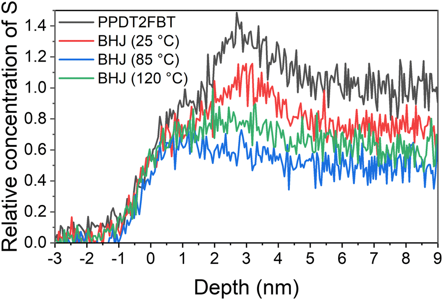 | ||
| Fig. 6 Concentration depth profiles of either pristine PPDT2FBT (black line) or PPDT2FBT:PC61BM BHJ (coloured lines). The BHJ is either non-annealed (25 °C) (red line), aged at 85 °C for 6 months (blue) or aged at 120 °C for 24 hours (green line). | ||
The sulphur concentration depth profile of the pure polymer (Fig. 6) shows a region at the surface and a second, high concentration region at 5–9 nm, which could be associated with polymer morphology. This same sulphur concentration dependence can be observed for the BHJ exposed to only 25 °C, however, the concentration is lower than in the pure polymer, indicating that the BHJ samples contain a mixture of polymer and PC61BM at the surface and bulk of the active layer. This depth dependence of sulphur disappears after annealing at 85 °C and 120 °C indicating a reduction of polymer and corresponding to an increase in PC61BM. To calculate the concentrate of sulphur, and in turn, the concentration of PPDT2FBT polymer and PC61BM in the bulk material, the step height of the sulphur and carbon were used. Step height values and relating composite values can be seen in Table 2.
:S step height ratio of pristine PPDT2FBT
| Sample | Step height (arb units) | S:C step height ratio |
Material composition | ||
|---|---|---|---|---|---|
| Sulphur | Carbon | Polymer (%) | Fullerene (%) | ||
| PPDT2FBT | 4800 | 65000 |
0.074 | 100 | 0 |
| BHJ 25 °C | 3900 | 71000 |
0.055 | 74 | 26 |
| BHJ 85 °C | 2800 | 77000 |
0.036 | 49 | 51 |
| BHJ 120 °C | 4000 | 89000 |
0.045 | 61 | 39 |
By calculating the material composition based on the S:C step height ratio, it was found that the bulk of the BHJ contained a mixture of polymer and fullerene materials. Based on theoretical calculations of PPDT2FBT polymer unit:fullerene molecule ratio based on a 1:2 w/w ratio, it is expected the unit:molecule ratio would be 1:9.5 throughout the entire layer. Instead, the calculated ratio is closer to 3:4, indicating that there is an enrichment of polymer at the surface. As seen in Table 2, the BHJ annealed at 85 °C has far less polymer at the near-surface (49%) compared to both the non-annealed and the 120 °C annealed samples (61%). Unlike 3-dimensional fullerene crystals that may have polymer at their surface due to either the migration process or formation of the said crystals near the surface of the active layer, it is suspect the flat features on the surface of the 85 °C annealed sample to be purely PC61BM within the effective depth of the NICISS. To support this argument, the percentage of PC61BM determined from the NICISS was compared with the surface area of the flat features observed from the SEM (seen in Fig. S15 in ESI†).
With the SEM image of the active layer surface, the bright area of the surface was measured with ImageJ, using the measure threshold function. From the images, it was found the surface area consisted of approximately 20% of flat fullerene features. From NICISS it can be seen that the bulk polymer composition decreases by approximately 20% from the non-annealed to the 85 °C aged BHJ sample. This is an increase of fullerene by the same amount, supporting the observation that the increase in fullerene at the surface and near-surface is from the flat features. By implementing SEM, AES and NICISS to investigate the flat features at the surface of the PPDT2FBT:PC61BM blend after being thermally aged 85 °C, the flat features are rich in PC61BM, while there is a depletion of polymer near the surface after annealing. As for 120 °C, the NICISS supports the observation from AES that there may be PPDT2FBT polymer on the surface of the 3-dimensional fullerene crystals. With composition of the crystals and features now determined for the thermally annealed PPDT2FBT:PC61BM films, the next step was to investigate how the thermal behaviour changes upon different ageing conditions, with the use of dynamic mechanical thermal analysis.
2.6. Thermal degradation behaviour
Dynamic mechanical thermal analysis (DMTA) is a technique that has been implemented for the investigation of the thermal behaviour of OPV active layer blends and is a useful method for understanding the thermal transitions of pure materials and blends, as well as a tool to understand the morphological change of the BHJ layer upon thermal annealing.81–83 In this work, this technique was used to investigate the thermal behaviour of the active layer blend reinforced with glass fibre.In a previous work, DMTA was demonstrated to show how the addition of C70 was able to influence the thermal properties of PPDT2FBT:PC61BM, resulting in the fullerene crystallisation to occur at a higher temperature.55 In this work, the purpose of the DMTA measurements was to observe how the thermal transitions changed after the samples experienced different temperatures and durations of annealing. It was hypothesised that, as the morphology changes, that there may be a shift in certain thermal transitions.
For pure PPDT2FBT polymer (seen in Fig. 7a), one sub-glass transition (sub-Tg) was observed at around −25 °C (having been determined from tan delta peak), while no clear Tg was detected with DMTA, indicating the lack of amorphous phase in the solid state,81 and similar phase behaviour had been reported for other high performing polymers.81,84 The lack of amorphous phase was further supported by previous work, where grazing-incidence wide angle x-ray scattering (GIWAXS) spectroscopy result showed the PPDT2FBT to be a partially crystallising polymer.58,85 There also appears a minor thermal transition that moves from 75 °C to 175 °C after annealing the DMTA samples at different temperatures.
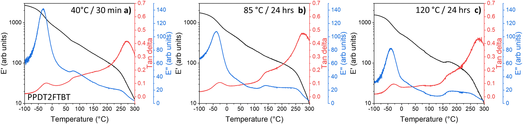 | ||
| Fig. 7 DMTA of pure PPDT2FBT after thermal annealing: (a) 40 °C for 30 minutes, (b) 85 °C for 24 hours, and (c) 120 °C for 24 hours. | ||
When the PPDT2FBT is subjected to annealing at elevated temperature for 24 hours prior to DMTA measurements (Fig. 7b and c), the transition at 75 °C appears to shift, with the feature located at 140 °C and 175 °C after annealing at 85 °C and 120 °C, respectively. For 120 °C exclusively, the feature at 175 °C is accompanied by an increase in E′. It is suspected that this feature is associated with the cold crystallisation of the PPDT2FBT. The shift of the peak could be associated with the polymer re-organising itself. As partially crystalline polymers may have several transitions present during heating, including Tg, cold crystallisation and melting.86 As the thickness of the polymer layer is adjusted, temperature that these transitions occur at including Tg87 and cold-crystallisation.86 Based on the DMTA results, the heating of the polymer likely leads to increased size of crystalline phase of PPDT2FBT, before cold-crystallisation happened. It is also found that the sub-Tg did not see any significant temperature shift, regardless of the change in pre-annealing conditions.
For the blend that has been annealed at 40 °C (to remove thermal history83) (Fig. 8a), one extra thermal relaxation at ∼100 °C, seen by the E′′ peak, as well as a thermal transition without stiffness change at ∼70 °C. After annealing the samples at 85 °C for 8 hours, it is observed that the ∼100 °C thermal relaxation peak shifts to ∼130 °C (Fig. 8b), while the thermal transition at ∼70 °C shifts to a lower temperature at ∼50 °C.
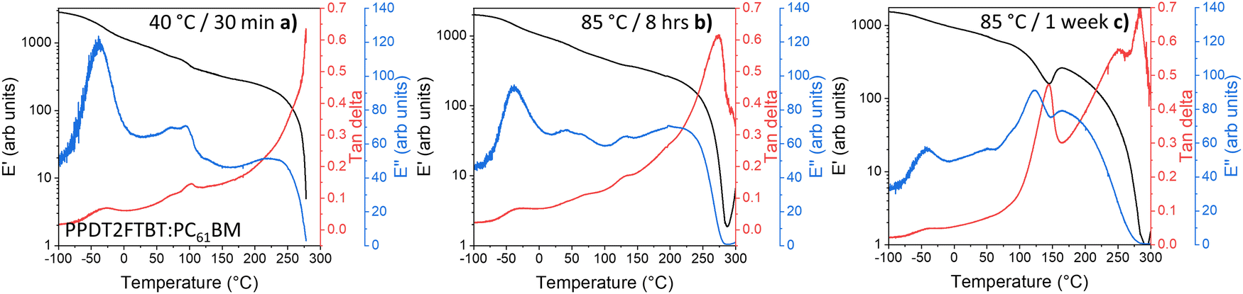 | ||
| Fig. 8 DMTA of PPDT2FBT:PC61BM samples after thermal annealing: (a) 40 °C for 30 minutes, as well as (b) 85 °C for 8 hours, and (c) 1 week. | ||
This shift in the ∼100 °C thermal relaxation is suspected to be associated with the cold crystallisation of PC61BM, especially when, after 1 week of pre-annealing at 85 °C (Fig. 8c) resulted in E′ increase from ∼100 °C to ∼145 °C, indicating the formation of crystals during the DMTA scan. This feature has also been reported in previous work, which attributed the E′ increase to the cold crystallisation of Y6 at 190 °C.88
As the SEM images showed a lack of 3-dimensional fullerenes on the 85 °C annealed PPDT2FBT:PC61BM surface, it can be speculated that this crystal formation occurred once a higher temperature was reached during the DMTA measurement. As such, the DMTA results supported the idea that annealing at 85 °C results in the change in morphology, allowing for purer PC61BM and polymer phases to form. Once these phases have increased in purity, and potentially in size, a substantial amount of crystallisation can be observed during DMTA measurement. The increase in the suspected PC61BM cold crystallisation temperature initially found at ∼100 °C and shifted at ∼130 °C is likely due to the increased size in fullerene phase. As discussed previously, there is a size dependency for thermal transitions.86,87 Based on these observations, as the blend is heated at 85 °C, the fullerene phase in the blend increases in size and purity, before reaching a point where, during the DMTA measurement, the cold crystallisation of fullerene can significantly influence the stiffness of the sample.
The last observation found with the 85 °C aged PPDT2FBT:PC61BM, is the feature at −25 °C, which is confirmed to be the sub-Tg of the PPDT2FBT polymer (seen in Fig. 7a). It does not appear to significantly shift in temperature position. With the axis of the E′′ kept constant, it appears that the height of the E′′ peak reduces as the PPDT2FBT:PC61BM blend is annealed at 85 °C, even after 30 minutes (as seen in Fig. S16 in ESI†). There is also a partial reduction of the E′′ peak when compared with pure PPDT2FBT polymer and it is consistent with better packing of the polymer chains after annealing as the side-chains have limited movement This embrittling of the Sub-Tg has been previously observed for TQ1:PC61BM, with a reduced tan delta signal related to the restricted movement of the polymer's side chains.81
Unlike the 85 °C pre-annealed PPDT2FBT:PC61BM blends, the samples that had experienced different annealing times at 120 °C (Fig. 9) resulted in the 100 °C thermal transition feature (seen in Fig. 8a) mostly disappearing. It is expected that during the annealing of the sample at the higher temperature the PC61BM undergoes crystallisation, resulting in no further cold crystallisation observed in the DMTA scan. It is also seen that there are minimal differences between the 120 °C annealed samples at various times (8 hours, 1 week), with it being attributed to the lack of morphology change after annealing for 8 hours (Fig. 9b).
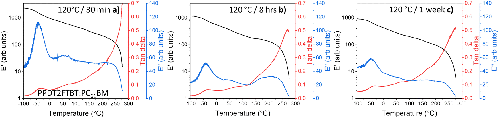 | ||
| Fig. 9 DMTA of PPDT2FBT:PC61BM samples after thermal annealing: (a) 120 °C for 30 minutes, (b) 8 hours, and (c) 1 week. | ||
3. Conclusion
In this work, it was observed that, when annealing the PPBT2FBT:PC61BM devices at two different temperatures, maximum working temperature (85 °C) and accelerated ageing temperature (120 °C), the dominating degradation pathway of the active layer appeared to be significantly different. This is evident by comparing the power conservation efficiency in relation to ageing time, with devices ageing at 120 °C experiencing a more significant reduction in OPV performances than that compared to 85 °C aged devices. The characterisation of thermal aged active layer with surface techniques, SEM, AES, NICISS, and 2D-stylus profilometry revealed that 120 °C annealing led to the formation of fullerene crystals, whereas 85 °C led to flat features that were rich in PC61BM.By implementing the DMTA technique to study the change in thermal behaviour after annealing the PPDT2FBT:PC61BM blends, it was found that the major degradation pathway at 120 °C is associated with fullerene crystallisation, while 85 °C resulted in significant changes to the morphology, with the increased phase separation between PPDT2FBT and PC61BM. This work clearly demonstrates that performing accelerating ageing at 120 °C is not suitable for PPBT2FBT:PC61BM devices and highlights the importance of performing thermal degradation studies at annealing temperatures that do not introduce new degradation pathways. From the DMTA measurements, with the support of SEM, AES and NICISS, it is clear that the two ageing temperatures (85 °C and 120 °C) affects the BHJ material differently. For 120 °C, large 3D fullerene crystallisation forms relatively quickly (within 24 hours), resulting in a significant decrease in device performance. Whereas for 85 °C aged materials, the degradation is more associated with the changes in morphology, resulting the movement of PPDT2FBT polymer side-chains being restricted, and slow increase in phase purity/size. This work clearly shows that care must be taken when performing accelerated ageing of OPV devices and materials, ensuring that the studied degradation pathways are the same as under operating conditions.
4. Experimental section
4.1. Materials
Donor material poly[(2,5-bis(2hexyldecyloxy)phenylene)-alt-(5,6-difluoro-4,7-di(thiophen-2-yl)benzo[c][1,2,5]thiadiazole)] (PPDT2FBT) was synthesised using a direct arylation polymerisation according to literature.89 The molecular weight of PPDT2FBT was determined via Gel Permeation Chromatography (Agilent 1260 Infinity II High-Temperature GPC System) using trichlorobenzene at 150 °C, giving a number average molecular weight (Mn) of 27 of kg mol−1 with a PDI of 3.5 relative to polystyrene standards.The ZnO nanoparticle (NP) dispersion ink was prepared based on a previously published procedure90 with some modifications. To achieve an ideal processing concentration, acetone (Chem-supply, 99.9%) was added to the NP precipitate until a concentration of approximately 35–40 mg mL−1 was achieved. Afterwards, 2-(2-methoxyethoxy)acetic acid (Sigma Aldrich) (5% w/w in relation to ZnO NP) was added to stabilise the NP dispersion. Further details can be found in ESI.†
Small molecule fullerene acceptor [6,6]-phenyl-C61-butyric acid ester (PC61BM) was purchased from Solenne BV. Solvents ortho-dichlorobenzene, chlorobenzene and 1-chloronaphthalene were purchased from Sigma Aldrich, whereas chloroform (CHCl3) was purchased from Chem-Supply. All solvents were used directly without purification.
4.2. Device fabrication
Slot-die coated devices were fabricated in a PET/ITO/ZnO NP/BHJ layer/MoOX/Al device configuration, where the BHJ layer was composed of a PPDT2FBT:PC61BM blend. Active layer ink was prepared by dissolving materials, with a donor:acceptor weight ratio of 1:2, in ortho-dichlorobenzene (total 25 mg mL−1 or 14 mg mL−1) with 0.5% V/V of 1-chloronaphthalene at 60 °C overnight under ambient conditions.
The flexible ITO substrate (50 Ohm sq−1, Dongguan Hongdian Technology Co.) was attached to a mini-roll coater (FOM technologies) with slot-die attachment (13 mm width meniscus guide) and wiped with isopropanol soaked TerriWipes at a rotation speed of 2 m min−1 prior to fabrication. The tubing and slot-die head was cleaned with chloroform prior to assembly and between the change of deposition material. Layer deposition was processed under ambient conditions.
The ZnO nanoparticle NP layer (35 nm) was deposited using 0.1 mL min−1 flow-rate, a drum speed of 1.0 m min−1 and drum temperature at 70 °C to achieve a strip width of around 13 mm. The BHJ layer (150–200 nm) was deposited via varying flow rate and drum speed at a drum temperature of 70 °C to obtain a strip width of around 13 mm. Wet and dry thickness for both the ZnO NP and BHJ layers were calculated according to eqn (S1) & (S2) in the ESI.†
After slot-die coating, the MoOX and aluminium was deposited via the following method. The MoOx (12 nm) was thermally deposited on the BHJ layer under high vacuum using a Covap thermal evaporation system (Angstrom Engineering). This was followed by the evaporation of the Al electrode (80 nm) using a shadow mask, defining the active area to 0.1 cm2.
Devices were measured using an Oriel Solar simulator fitted with a 150 W Xeon lamp (Newport), filtered to give an output of 100 mW cm−2 at AM 1.5 (air mass) standard and calibrated using a silicon reference cell with NIST traceable certification. Device testing was conducted under ambient conditions. The photocurrent–voltage (I–V) characteristics of the devices were measured through a Keithley 2450 source meter unit. For investigating performance and material degradation, PET/ITO/ZnO NP/BHJ layer/MoOX/Al & PET/ITO/ZnO NP/BHJ device configurations were used, respectively. Thermal annealing and ageing were conducted on a hotplate in a nitrogen-filled glove-box with minimal light exposure.
4.3. Charge carrier dynamics
Photoinduced charge extraction by linearly increasing voltage (photoCELIV), transient photovoltage (TPV) and time-resolved charge extraction (TRCE) measurements were conducted using a commercially available PAIOS 2 system (Fluxim AG). For carrier transport determined via photoCELIV, a light pulse from a white LED (Cree, xp-g) was used to put devices into an open circuit condition, with the removal of light simultaneous with the application of a linearly increasing reverse bias voltage (50 V ms−1). For charge carrier lifetime measurements, the devices were placed into an open circuit condition under illumination and then a small light pulse was used to induce a transient increase in photovoltage (∼5 mV), with the decay of the voltage back to VOC fitted to determine the lifetime. The charge density generated in the devices under illumination was determined via TRCE, where devices were held in an open circuit condition under illumination, with removal of light simultaneous with a square-step reverse bias extraction voltage. The current transients were recorded by the integrated PAIOS hardware.4.4. Scanning electron microscopy
Measurements were performed using Inspect F50 scanning electron microscopy (SEM) (https://doi.org/10.25957/flinders.sem) equipped with a field emission gun (FEI Company) and a secondary electron detector. The acceleration voltage was 10 kV, and the working distance of 10 mm. The samples were not coated with any conducting layers. ImageJ was used to analyse the surface features that were observed on the thermally aged samples.4.5. Stylus profilometry
Measurements were performed using the Bruker DektakXT stylus profilometer, equipped with a 2 μm probe, and 2-dimensional stage movement controllers. The vertical measurement range of the profilometer was set to 6.5 μm, with a vertical resolution of 0.1 nm.4.6. Auger electron spectroscopy
Measurements were performed using a PHI 710 Scanning Auger Nanoprobe system. The acceleration voltage was 10 kV and emission current were 1 nA. Spectra were collected via point (0.65 μm diameter) scans as specific locations on the sample (SEM images of scan locations can be found in the ESI†). The Auger spectra were filtered and analysed, as well as element concentrations calculated with MultiPak Spectrum. The peak height to atomic concentration values for specific elements were based on previously published work.744.7. Neutral impact collision ion scattering spectroscopy
Elemental depth profiling at a depth resolution of a few Angstroms (Å) was performed using neutral impact collision ion scattering spectroscopy (NICISS) with the details of the data evaluation described in previous publications.76,78,91 Pulses of positively-charge helium ions with a kinetic energy of 3 keV were used as projectiles. Projectiles backscattered from the sample are detected with a time-of-flight (ToF) detector, with a count rate of approximately 200 counts per second. In the NICISS results, the different elements in the sample are represented as peaks and steps. The photon peak is the first peak in the NICISS spectrum which corresponds to the first interaction between He+ and the sample surface resulting in the emission of photons with a TOF of 4 ns. In concentration depth profiles count rate can be found at negative depth in non-deconvoluted NICISS, which has a lack of physical significance. This phenomenon is associated with the finite energy resolution of the method which is discussed in detail in a paper by Zhao et al.92 Analysis of NICISS spectra is based on previous literature that had determined the composition of the surface and near surface of a blend of P3HT:PCBM, identifying a layered structure at the surface.76 The known bulk concentration of a sample is used to convert the measured count rate into concentration.934.8. Dynamic mechanical thermal analysis
The dynamic mechanical thermal analysis (DMTA) was conducted on a DMA Q800 (TA Instruments) equipped with a liquid nitrogen cooling apparatus. The DMTA samples were prepared by repeatedly drop-casting the respective solutions on pre-cut glass mesh as described in previous literature.81,94 Sample preparation and instrument conditions can be found in ESI.† Preheating of samples were performed under dark, nitrogen conditions.Author contributions
Bradley Kirk worked on device fabrication and material characteristic measurements, as well as writing of the draft paper. Amira R. Alghamdi ran NICISS measurements on the active layer materials, as well as results discussion and interpretation with other surface analysis techniques. Matthew J. Griffith ran the charge carrier behaviour measurements (photoCELIV, TPV and TRCE), results discussion and interpretation. Xun Pan prepared samples and performed DMTA measurements on active material blends, as well as results discussion and interpretation. Martyn Jevric synthesised and characterised the PPDT2FBT polymer used in OPV fabrication. David Lewis provided funding and guidance through the work. Gunther Andersson provided helped with guidance and expert advice throughout the work. Mats Andersson provided funding and resources towards the work, as well as guidance through the work. All the authors contributed to the correction and revision of the manuscript.Data availability statement
The data that support the findings of this study are available from the corresponding author upon reasonable request.Conflicts of interest
There is no conflict to declare.Acknowledgements
The authors acknowledge the Commonwealth of Australia through the access from the Australian Government Research Training Program (AGRTP) for providing funding to undertake a PhD Higher Degree Research program, with addition to Playford Trust for providing additional funding towards the research program. This activity received funding from the Australian Research Council's Discovery Projects (DP 220102900, DP230102705) and Future Fellowship (FT230100154) funding schemes, as well as ARENA as part of ARENA's Research and Development Program-Solar PV Research. We acknowledge Flinders Microscopy and Microanalysis (FMMA) at Flinders University for providing access to the microscopy instrument and facilities. Additionally, the authors acknowledge the scientific and technical assistance of Microscopy Australia staff at the University of South Australia, a facility that is co-funded by the University of South Australia, the State and Federal Governments. This work was performed in part at the South Australian node the Australian National Fabrication Facility (ANFF) under the National Collaborative Research Infrastructure Strategy.References
- B. C. Thompson and J. M. J. Fréchet, Angew. Chem., Int. Ed., 2008, 47, 58–77 CrossRef CAS PubMed.
- P. M. Beaujuge and J. M. J. Fréchet, J. Am. Chem. Soc., 2011, 133, 20009–20029 CrossRef CAS PubMed.
- T. R. Andersen, F. Almyahi, N. A. Cooling, D. Elkington, L. Wiggins, A. Fahy, K. Feron, B. Vaughan, M. J. Griffith and A. J. Mozer, J. Mater. Chem. A, 2016, 4, 15986–15996 RSC.
- L. Zhu, M. Zhang, J. Xu, C. Li, J. Yan, G. Zhou, W. Zhong, T. Hao, J. Song, X. Xue, Z. Zhou, R. Zeng, H. Zhu, C.-C. Chen, R. C. I. MacKenzie, Y. Zou, J. Nelson, Y. Zhang, Y. Sun and F. Liu, Nat. Mater., 2022, 21, 656–663 CrossRef CAS PubMed.
- Y. Wei, Z. Chen, G. Lu, N. Yu, C. Li, J. Gao, X. Gu, X. Hao, G. Lu, Z. Tang, J. Zhang, Z. Wei, X. Zhang and H. Huang, Adv. Mater., 2022, 34, 2204718 CrossRef CAS PubMed.
- A. Distler, C. J. Brabec and H.-J. Egelhaaf, Prog. Photovoltaics Res. Appl., 2021, 29, 24–31 CrossRef.
- M. Ylikunnari, M. Välimäki, K.-L. Väisänen, T. M. Kraft, R. Sliz, G. Corso, R. Po, R. Barbieri, C. Carbonera, G. Gorni and M. Vilkman, Flexible Printed Electron., 2020, 5, 014008 CrossRef CAS.
- S. V. Dayneko, M. Pahlevani and G. C. Welch, ACS Appl. Mater. Interfaces, 2019, 11, 46017–46025 CrossRef CAS PubMed.
- H. S. Ryu, S. Y. Park, T. H. Lee, J. Y. Kim and H. Y. Woo, Nanoscale, 2020, 12, 5792–5804 RSC.
- N. Cooling, E. Barnes, F. Almyahi, K. Feron, M. Al-Mudhaffer, A. Al-Ahmad, B. Vaughan, T. Andersen, M. Griffith and A. Hart, J. Mater. Chem. A, 2016, 4, 10274–10281 RSC.
- R. Søndergaard, M. Hösel, D. Angmo, T. T. Larsen-Olsen and F. C. Krebs, Mater. Today, 2012, 15, 36–49 CrossRef.
- Z. Zhang, J. Miao, Z. Ding, B. Kan, B. Lin, X. Wan, W. Ma, Y. Chen, X. Long, C. Dou, J. Zhang, J. Liu and L. Wang, Nat. Commun., 2019, 10, 3271 CrossRef PubMed.
- N. Zheng, K. Mahmood, W. Zhong, F. Liu, P. Zhu, Z. Wang, B. Xie, Z. Chen, K. Zhang, L. Ying, F. Huang and Y. Cao, Nano Energy, 2019, 58, 724–731 CrossRef CAS.
- R. Meitzner, T. Faber, S. Alam, A. Amand, R. Roesch, M. Büttner, F. Herrmann-Westendorf, M. Presselt, L. Ciammaruchi and I. Visoly-Fisher, Sol. Energy Mater. Sol. Cells, 2019, 202, 110151 CrossRef CAS.
- M. Li, W. Zhang, H. Wang, L. Chen, C. Zheng and R. Chen, RSC Adv., 2017, 7, 31158–31163 RSC.
- C.-N. Weng, H.-C. Yang, C.-Y. Tsai, S.-H. Chen, Y.-S. Chen, C.-H. Chen, K.-M. Huang, H.-F. Meng, Y.-C. Chao and C.-Y. Chang, Sol. Energy, 2020, 199, 308–316 CrossRef CAS.
- N. Y. Doumon, G. Wang, R. C. Chiechi and L. J. A. Koster, J. Mater. Chem. C, 2017, 5, 6611–6619 RSC.
- B. Muhsin, R. Roesch, G. Gobsch and H. Hoppe, Sol. Energy Mater. Sol. Cells, 2014, 130, 551–554 CrossRef CAS.
- B. Zimmermann, H.-F. Schleiermacher, M. Niggemann, U. Würfel and S. Cells, Sol. Energy Mater. Sol. Cells, 2011, 95, 1587–1589 CrossRef CAS.
- Y. Sun, L. Meng, X. Wan, Z. Guo, X. Ke, Z. Sun, K. Zhao, H. Zhang, C. Li and Y. Chen, Adv. Funct. Mater., 2021, 31, 2010000 CrossRef CAS.
- H. Kang, G. Kim, J. Kim, S. Kwon, H. Kim and K. Lee, Adv. Mater., 2016, 28, 7821–7861 CrossRef CAS PubMed.
- W. Greenbank, N. Djeddaoui, E. Destouesse, J. Lamminaho, M. Prete, L. Boukezzi, T. Ebel, L. Bessissa, H.-G. Rubahn, V. Turkovic and M. Madsen, Energy Technol., 2020, 8, 2000295 CrossRef CAS.
- L. Duan and A. Uddin, Adv. Sci., 2020, 7, 1903259 CrossRef CAS PubMed.
- B. Paci, A. Generosi, V. Rossi Albertini, P. Perfetti, R. de Bettignies, J. Leroy, M. Firon and C. Sentein, Appl. Phys. Lett., 2006, 89, 043507 CrossRef.
- J. W. Andreasen, S. A. Gevorgyan, C. M. Schlepütz and F. C. Krebs, Sol. Energy Mater. Sol. Cells, 2008, 92, 793–798 CrossRef CAS.
- W. Greenbank, N. Rolston, E. Destouesse, G. Wantz, L. Hirsch, R. Dauskardt and S. Chambon, J. Mater. Chem. A, 2017, 5, 2911–2919 RSC.
- Y. M. Sung, Y. C. Huang, F. S. S. Chien and C. S. Tsao, IEEE J. Photovolt., 2019, 9, 694–699 Search PubMed.
- W. Greenbank, L. Hirsch, G. Wantz and S. Chambon, Appl. Phys. Lett., 2015, 107, 263301 CrossRef.
- M. O. Reese, S. A. Gevorgyan, M. Jørgensen, E. Bundgaard, S. R. Kurtz, D. S. Ginley, D. C. Olson, M. T. Lloyd, P. Morvillo, E. A. Katz, A. Elschner, O. Haillant, T. R. Currier, V. Shrotriya, M. Hermenau, M. Riede, K. R. Kirov, G. Trimmel, T. Rath, O. Inganäs, F. Zhang, M. Andersson, K. Tvingstedt, M. Lira-Cantu, D. Laird, C. McGuiness, S. Gowrisanker, M. Pannone, M. Xiao, J. Hauch, R. Steim, D. M. DeLongchamp, R. Rösch, H. Hoppe, N. Espinosa, A. Urbina, G. Yaman-Uzunoglu, J.-B. Bonekamp, A. J. J. M. van Breemen, C. Girotto, E. Voroshazi and F. C. Krebs, Sol. Energy Mater. Sol. Cells, 2011, 95, 1253–1267 CrossRef CAS.
- N. Chaturvedi, N. Gasparini, D. Corzo, J. Bertrandie, N. Wehbe, J. Troughton and D. Baran, Adv. Funct. Mater., 2021, n/a, 2009996 CrossRef.
- J. Wu, X. Guo, M. Xiong, X. Xia, Q. Li, J. Fang, X. Yan, Q. Liu, X. Lu, E. Wang, D. Yu and M. Zhang, Chem. Eng. J., 2022, 446, 137424 CrossRef CAS.
- S. B. Sapkota, A. Spies, B. Zimmermann, I. Dürr and U. Würfel, Sol. Energy Mater. Sol. Cells, 2014, 130, 144–150 CrossRef CAS.
- S. A. Gevorgyan, M. Corazza, M. V. Madsen, G. Bardizza, A. Pozza, H. Müllejans, J. C. Blakesley, G. F. A. Dibb, F. A. Castro, J. F. Trigo, C. M. Guillén, J. R. Herrero, P. Morvillo, M. G. Maglione, C. Minarini, F. Roca, S. Cros, C. Seraine, C. H. Law, P. S. Tuladhar, J. R. Durrant and F. C. Krebs, Polym. Degrad. Stab., 2014, 109, 162–170 CrossRef CAS.
- L. Hong, H. Yao, Y. Cui, R. Yu, Y.-W. Lin, T.-W. Chen, Y. Xu, J. Qin, C.-S. Hsu, Z. Ge and J. Hou, Small, 2021, 17, 2101133 CrossRef CAS PubMed.
- K. Ding, Y. Li and S. R. Forrest, ACS Appl. Mater. Interfaces, 2022, 14, 5692–5698 CrossRef CAS PubMed.
- Y. Xu, J. Yuan, S. Zhou, M. Seifrid, L. Ying, B. Li, F. Huang, G. C. Bazan and W. Ma, Adv. Funct. Mater., 2019, 29, 1806747 CrossRef.
- M. Kim, S. Park, D. Y. Ryu and K. Kim, Polymer, 2016, 103, 132–139 CrossRef CAS.
- S. Park, S. H. Park, H. Jin, S. Yoon, H. Ahn, S. Shin, K. Kwak, S. Nah, E.-Y. Shin, J. H. Noh, B. K. Min and H. J. Son, Nano Energy, 2022, 98, 107187 CrossRef CAS.
- H. J. Son, H.-K. Park, J. Y. Moon, B.-K. Ju and S. H. Kim, Sustainable Energy Fuels, 2020, 4, 1974–1983 RSC.
- Z. Li, K. Ho Chiu, R. Shahid Ashraf, S. Fearn, R. Dattani, H. Cheng Wong, C.-H. Tan, J. Wu, J. T. Cabral and J. R. Durrant, Sci. Rep., 2015, 5, 15149 CrossRef CAS PubMed.
- M. Bolognesi, M. Prosa, M. Tessarolo, G. Donati, S. Toffanin, M. Muccini and M. Seri, Sol. Energy Mater. Sol. Cells, 2016, 155, 436–445 CrossRef CAS.
- H. Lee, J. Sohn, P. Tyagi and C. Lee, Appl. Phys. Lett., 2017, 110, 053301 CrossRef.
- Z. Wang, Y. Nian, H. Jiang, F. Pan, Z. Hu, L. Zhang, Y. Cao and J. Chen, Org. Electron., 2019, 69, 174–180 CrossRef.
- Y. He, T. Heumüller, W. Lai, G. Feng, A. Classen, X. Du, C. Liu, W. Li, N. Li and C. J. Brabec, Adv. Energy Mater., 2019, 9, 1900409 CrossRef.
- K. Xian, S. Zhang, Y. Xu, J. Liu, K. Zhou, Z. Peng, M. Li, W. Zhao, Y. Chen, Z. Fei, J. Hou, Y. Geng and L. Ye, Sci. China: Chem., 2023, 66, 202–215 CrossRef CAS.
- Z. Wang, Z. Hong, T. Zhuang, G. Chen, H. Sasabe, D. Yokoyama and J. Kido, Appl. Phys. Lett., 2015, 106, 053305 CrossRef.
- X. Xu, K. Fukuda, A. Karki, S. Park, H. Kimura, H. Jinno, N. Watanabe, S. Yamamoto, S. Shimomura and D. Kitazawa, Proc. Natl. Acad. Sci. U. S. A., 2018, 115, 4589–4594 CrossRef CAS PubMed.
- S. Song, K. T. Lee, C. W. Koh, H. Shin, M. Gao, H. Y. Woo, D. Vak and J. Y. Kim, Energy Environ. Sci., 2018, 11, 3248–3255 RSC.
- J. Yin, W. Zhou, L. Zhang, Y. Xie, Z. Yu, J. Shao, W. Ma, J. Zeng and Y. Chen, Macromol. Rapid Commun., 2017, 38, 1700428 CrossRef PubMed.
- C. Zhang, A. Mumyatov, S. Langner, J. D. Perea, T. Kassar, J. Min, L. Ke, H. Chen, K. L. Gerasimov, D. V. Anokhin, D. A. Ivanov, T. Ameri, A. Osvet, D. K. Susarova, T. Unruh, N. Li, P. Troshin and C. J. Brabec, Adv. Energy Mater., 2017, 7, 1601204 CrossRef.
- Y.-C. Chao, C.-H. Chuang, H.-L. Hsu, H.-J. Wang, Y.-C. Hsu, C.-P. Chen and R.-J. Jeng, Sol. Energy Mater. Sol. Cells, 2016, 157, 666–675 CrossRef CAS.
- T. M. Grant, T. Gorisse, O. Dautel, G. Wantz and B. H. Lessard, J. Mater. Chem. A, 2017, 5, 1581–1587 RSC.
- W. Feng, Z. Lin, J. Cui, W. Lv, W. Wang and Q. Ling, Sol. Energy Mater. Sol. Cells, 2019, 200, 109982 CrossRef CAS.
- Y. Jang, Y. Ju Cho, M. Kim, J. Seok, H. Ahn and K. Kim, Sci. Rep., 2017, 7, 9690 CrossRef PubMed.
- B. Kirk, X. Pan, M. Jevric, G. Andersson and M. R. Andersson, Mater. Adv., 2022, 3, 2838–2849 RSC.
- Z. Du, M. Mainville, J. Vollbrecht, A. L. Dixon, N. Schopp, M. Schrock, Z. Peng, J. Huang, S. Chae, H. Ade, M. Leclerc, G. N. M. Reddy and T.-Q. Nguyen, Sol. RRL, 2021, 5, 2100213 CrossRef CAS.
- M. Mainville, V. Tremblay, M. Z. Fenniri, A. Laventure, M. E. Farahat, R. Ambrose, G. C. Welch, I. G. Hill and M. Leclerc, Asian J. Org. Chem., 2020, 9, 1318–1325 CrossRef CAS.
- T. L. Nguyen, H. Choi, S. J. Ko, M. A. Uddin, B. Walker, S. Yum, J. E. Jeong, M. H. Yun, T. J. Shin and S. Hwang, Energy Environ. Sci., 2014, 7, 3040–3051 RSC.
- T. L. Nguyen, H. Choi, S. J. Ko, M. A. Uddin, B. Walker, S. Yum, J. E. Jeong, M. H. Yun, T. J. Shin, S. Hwang, J. Y. Kim and H. Y. Woo, Energy Environ. Sci., 2014, 7, 3040–3051 RSC.
- J. Zhao, A. Swinnen, G. Van Assche, J. Manca, D. Vanderzande and B. V. Mele, J. Phys. Chem. B, 2009, 113, 1587–1591 CrossRef CAS PubMed.
- S. Bertho, G. Janssen, T. J. Cleij, B. Conings, W. Moons, A. Gadisa, J. D’Haen, E. Goovaerts, L. Lutsen and J. Manca, Sol. Energy Mater. Sol. Cells, 2008, 92, 753–760 CrossRef CAS.
- R. Sun, D. Deng, J. Guo, Q. Wu, J. Guo, M. Shi, K. Shi, T. Wang, L. Xue and Z. Wei, Energy Environ. Sci., 2019, 12, 2518–2528 RSC.
- R. De Bettignies, J. Leroy, M. Firon and C. Sentein, Synth. Met., 2006, 156, 510–513 CrossRef CAS.
- S. Schuller, P. Schilinsky, J. Hauch and C. J. Brabec, Appl. Phys. A: Mater. Sci. Process., 2004, 79, 37–40 CrossRef CAS.
- S. A. Gevorgyan, M. Jørgensen and F. C. Krebs, Sol. Energy Mater. Sol. Cells, 2008, 92, 736–745 CrossRef CAS.
- B. Chang, H.-W. Cheng, Y.-C. Lin, H.-C. Wang, C.-H. Chen, V.-T. Nguyen, Y. Yang and K.-H. Wei, ACS Appl. Mater. Interfaces, 2020, 12, 55023–55032 CrossRef CAS PubMed.
- L. Y. Su, H. H. Huang, Y. C. Lin, G. L. Chen, W. C. Chen, W. Chen, L. Wang and C. C. Chueh, Adv. Funct. Mater., 2021, 31, 2005753 CrossRef CAS.
- O. Haillant, D. Dumbleton and A. Zielnik, Sol. Energy Mater. Sol. Cells, 2011, 95, 1889–1895 CrossRef CAS.
- M. J. Tan, W.-P. Goh, J. Li, G. Pundir, V. Chellappan and Z.-K. Chen, ACS Appl. Mater. Interfaces, 2010, 2, 1414–1420 CrossRef CAS PubMed.
- B. C. O'Regan, J. R. Durrant, P. M. Sommeling and N. J. Bakker, J. Phy. Chem. C, 2007, 111, 14001–14010 CrossRef.
- O. Oklobia and T. S. Shafai, Sol. Energy Mater. Sol. Cells, 2014, 122, 158–163 CrossRef CAS.
- R. A. Marsh, J. M. Hodgkiss, S. Albert-Seifried and R. H. Friend, Nano Lett., 2010, 10, 923–930 CrossRef CAS PubMed.
- Y. Shen, K. Li, N. Majumdar, J. C. Campbell and M. C. Gupta, Sol. Energy Mater. Sol. Cells, 2011, 95, 2314–2317 CrossRef CAS.
- K. D. Childs, B. A. Carlson, L. A. LaVanier, J. F. Moulder, D. F. Paul, W. F. Stickle and D. G. Watson, Handbook of Auger Electron Microscopy, Physical Electronics, Inc., Eden Prairie, Minnesota, 3rd edn, 1997 Search PubMed.
- H. Zhong, X. Yang, B. deWith and J. Loos, Macromolecules, 2006, 39, 218–223 CrossRef CAS.
- N. Schmerl and G. Andersson, Phys. Chem. Chem. Phys., 2011, 13, 14993–15002 RSC.
- H. L. Tan, T. Krebs, G. Andersson, D. Neff, M. Norton, H. Morgner and P. G. Van Patten, Langmuir, 2005, 21, 2598–2604 CrossRef CAS PubMed.
- A. R. Alghamdi, B. P. Kirk, G. Kocak, M. R. Andersson and G. G. Andersson, Molecules, 2022, 27, 6358 CrossRef CAS PubMed.
- D. Simatos, I. E. Jacobs, I. Dobryden, M. Nguyen, A. Savva, D. Venkateshvaran, M. Nikolka, J. Charmet, L. J. Spalek, M. Gicevičius, Y. Zhang, G. Schweicher, D. J. Howe, S. Ursel, J. Armitage, I. B. Dimov, U. Kraft, W. Zhang, M. Alsufyani, I. McCulloch, R. M. Owens, P. M. Claesson, T. P. J. Knowles and H. Sirringhaus, Small Methods, 2023, 7, 2300476 CrossRef CAS PubMed.
- G. Andersson and H. Morgner, Surf. Sci., 2000, 445, 89–99 CrossRef CAS.
- A. Sharma, X. Pan, J. M. Bjuggren, D. Gedefaw, X. Xu, R. Kroon, E. Wang, J. A. Campbell, D. A. Lewis and M. R. Andersson, Chem. Mater., 2019, 31, 6740–6749 CrossRef CAS.
- L. Yu, D. Qian, S. Marina, F. A. A. Nugroho, A. Sharma, S. Hultmark, A. I. Hofmann, R. Kroon, J. Benduhn and D.-M. Smilgies, ACS Appl. Mater. Interfaces, 2019, 11, 21766–21774 CrossRef CAS PubMed.
- X. Pan, A. Sharma, D. Gedefaw, R. Kroon, A. D. de Zerio, N. P. Holmes, A. L. D. Kilcoyne, M. G. Barr, A. Fahy and M. Marks, Org. Electron., 2018, 59, 432–440 CrossRef CAS.
- N. Balar, S. Siddika, S. Kashani, Z. Peng, J. J. Rech, L. Ye, W. You, H. Ade and B. T. O’Connor, Chem. Mater., 2020, 32, 6540–6549 CrossRef CAS.
- S.-C. Shin, C. W. Koh, P. Vincent, J. S. Goo, J.-H. Bae, J.-J. Lee, C. Shin, H. Kim, H. Y. Woo and J. W. Shim, Nano Energy, 2019, 58, 466–475 CrossRef CAS.
- B. Hajduk, H. Bednarski and B. Trzebicka, J. Phys. Chem. B, 2020, 124, 3229–3251 CrossRef CAS PubMed.
- A. El Ouakili, G. Vignaud, E. Balnois, J.-F. Bardeau and Y. Grohens, Thin Solid Films, 2011, 519, 2031–2036 CrossRef CAS.
- X. Pan, J. M. Bjuggren, M. Jevric, W. L. Tan, C. R. McNeill and M. R. Andersson, Chem. Mater., 2022, 34, 5103–5115 CrossRef CAS.
- P.-O. Morin, T. Bura, B. Sun, S. I. Gorelsky, Y. Li and M. Leclerc, ACS Macro Lett., 2015, 4, 21–24 CrossRef CAS PubMed.
- F. C. Krebs, Sol. Energy Mater. Sol. Cells, 2008, 92, 715–726 CrossRef CAS.
- A. R. Alghamdi, J. M. Bjuggren, X. Pan, M. R. Andersson and G. G. Andersson, Macromol. Mater. Eng., 2022, 307, 2200303 CrossRef CAS.
- X. Zhao, G. M. Nathanson and G. G. Andersson, J. Phys. Chem. B, 2020, 124, 2218–2229 CrossRef CAS PubMed.
- G. Andersson and H. Morgner, Surf. Sci., 1998, 405, 138–151 CrossRef CAS.
- A. Sharma, X. Pan, J. A. Campbell, M. R. Andersson and D. A. Lewis, Macromolecules, 2017, 50, 3347–3354 CrossRef CAS.
Footnote |
| † Electronic supplementary information (ESI) available. See DOI: https://doi.org/10.1039/d4ma00170b |
| This journal is © The Royal Society of Chemistry 2024 |