
 Open Access Article
 This Open Access Article is licensed under a
 Creative Commons Attribution 3.0 Unported Licence
Enhanced photoelectrochemical water splitting using nanostructured films: p-CuO sensitized with polyhedral n-Cu2O particles and CuS as photocathode†
Hugo Leandro Sousa
Santos
and
Lucia Helena
Mascaro
 *
*
Department of Chemistry, Federal University of São Carlos, Rod. Washington Luiz, Km 235, 13565-905, São Carlos-SP, Brazil. E-mail: lmascaro@ufscar.br
First published on 18th July 2024
Abstract
The harnessing of solar energy to produce high-density energy carriers, such as hydrogen, through cost-effective technologies like photoelectrochemical cells (PECs), has emerged as a significant and promising effort. In this study, we employed p-CuO nanostructures, functionalized with polyhedral n-CuO and CuS particles, as a photocathode for water splitting. The fabrication process involved depositing copper onto FTO substrates via electrodeposition, followed by anodization to generate Cu(OH)2 nanoneedles, which were subsequently transformed into CuO nanowires through annealing. Copper(I) oxide particles and CuS were deposited onto the CuO nanowires by electrodeposition and successive ionic layer adsorption and reaction (SILAR), respectively. The best CuO/Cu2O/CuS film demonstrated a remarkable photocurrent of −2.74 mA cm−2 at 0 VRHE. In summary, the formation of a type II p–n heterojunction between CuO and Cu2O facilitated improved charge separation, while the presence of CuS catalyzed the hydrogen evolution reaction (HER), highlighting the promising potential of this system for solar-driven hydrogen production.
Introduction
The future depletion of fossil fuels and the pollution generated by their indiscriminate consumption shows the need to find alternative energy carriers that are self-sufficient, renewable, and environmentally friendly.1 In this context, the solar energy has garnered a lot of attention due to the almost endless energy capacity of the sun.2,3 Furthermore, the use of solar energy to produce high density energy carriers like hydrogen from low-cost technologies such as photoelectrochemical cells (PECs), has proven to be important.3,4 Semiconductors used in photovoltaic cells have been employed as photoelectrodes in PEC water splitting. These materials present some disadvantages, such as high toxicity, difficult to obtain and, in their majority, are composed of elements scarce in the earth's crust such as Ga, In and Cd.5,6 Thus, transition metal oxides with low toxicity and structural complexity, composed of abundant and easily obtainable elements such as TiO2,7 WO3,8,9 Fe2O3,10 Cu2O,11,12 and CuO13,14 have emerged as promising alternatives to semiconductors made from toxic and scarce materials. Despite exhibiting lower efficiency in direct solar light conversion, these materials have shown promising results as photoelectrodes applied in PEC. Among the examples cited, copper oxides (CuO and Cu2O) have attracted considerable attention due to their high abundance in the Earth's crust, ease of synthesis, low cost, low toxicity.The structural and electronic differences between copper oxides lead them to different optoelectronic properties. In this regard, cupric oxide (CuO) is a p-type semiconductor that exhibits a small indirect Eg that can range between 1.3 and 1.8 eV, depending on the preparation method and morphology.15–17 Cuprous oxide (Cu2O), on the other hand, can exhibit p-type or n-type conductivity, depending on the synthesis method,18 and its direct Eg can range from 1.9 to 2.2 eV.19,20 Because of their excellent properties, copper oxides have been intensively studied as photocathodes or as photoanodes heterostructures, as in ZnO/Cu2O/Co–Pi,21 for water splitting. However, due to some deficiencies such as high recombination of charge carriers,22 a short electron diffusion length,23 and low chemical stability under the PEC reaction conditions, these semiconductors show much lower photoelectrocatalytic activities than theoretically predicted.
In recent years, great efforts have been made to enhance the activity and stability of copper oxides through heterojunctions, dual-photoelectrode tandem PEC cells, protective layers, and co-catalysts.22,24–26 Heterojunctions like p-Cu2O/p-CuO20,27 which can be easy synthesized by thermal oxidation of Cu2O layer28 and p-Cu2O/n-Cu2O18,29 have been widely discussed in the literature. However, p-CuO/n-Cu2O although it has been used in photovoltaic systems and presents band structures suitable for a type II heterojunction, there are still no publications in the literature of this system with photoelectrochemical applications.30,31
In addition, both CuO and Cu2O exhibit a small diffusion path of the photogenerated electrons, and these are not compatible with the photon absorption depth, this deficiency is one of the main reasons for the high electron–hole pair recombination in these materials.32 A way to get around this problem is by producing “1D structures” such as nanowires. These structures form a facilitated path for the diffusion of photogenerated electrons and holes and reduce the recombination of these charge carriers.32,33 In addition, the trapping of light by the nanostructures can lead to increased light absorption for the material. Furthermore, the high surface area provided by nanostructures generally leads to a larger electroactive area and higher efficiencies compared to smooth electrodes.33
The use of cocatalysts is another good way to increase the efficiency and stability of photoelectrodes. As alternatives to noble metals, cocatalysts based on abundant and inexpensive elements such as sulfides have been studied.22,27,34 In this regard, copper sulfide (CuS) has been used as a cocatalyst for photoelectrochemical systems that employ copper oxides as photocathodes.22,27 The improved photoelectrocatalytic activity of devices that use CuS as cocatalyst has been attributed not only to the higher charge transfer rate at the photoelectrode/electrolyte interface, but also to the inhibition of photocorrosion processes of copper oxides.
Herein, the production of nanostructured films of p-CuO as the main absorber layer modified with n-Cu2O particles and CuS cocatalyst applied as a photocathode for water splitting was reported.
Experimental
Materials and reagents
All chemicals were of analytical grade and used without any purification. F-Doped SnO2 (FTO) substrates with a resistance of 7 Ω sq−1, CuCl2·2H2O (99.8%), copper(II) acetate (98.0%), Na2S·9H2O (≥98.0%), Na2SO4 (≥99.0%), and NaOH (98.0%) were purchased from Sigma Aldrich.Production of CuO wires
First, thin films of metallic copper were electrodeposited on the FTO substrates. Before that, the substrates (1.5 × 1.0 cm) were cleaned in acetone, isopropanol, and ethanol (in this sequence) for 10 min in an ultrasonic bath and immersed, with the conductive faces facing upwards, in a solution of 25% NH3 and 30% H2O2 in a 1![[thin space (1/6-em)]](https://www.rsc.org/images/entities/char_2009.gif) :1 ratio (v/v) at 65 °C for 60 min. The electrodepositions were carried out on a 3-eletrode cell with an Ag/AgCl/KClsat. as reference electrode and a copper sheet (99.9%) as a counter-electrode. The electrodeposition bath was 0.1 mol L−1 CuCl2·2H2O and 0.2 mol L−1 glycine with the pH adjusted to 10.35 The bath temperature was 45 °C and N2 gas was bubbled throughout the experiment. The electrodeposition was accomplished applying a constant potential of −1.1 V until the charge density of −3.0 C cm−2. Then, Cu(OH)2 needles was produced by anodization in a 3-eletrode cell with a large area Pt grid as counter-electrode. The electrolyte was a 3 mol L−1 NaOH solution at the temperature of 25 °C. The Cu films were anodized applying a constant current density of 10 mA cm−2 until reaching the work electrode compliance potential of 0 V. This value was chosen based on its impact on film adherence. A more positive compliance potential was observed to lead to film detachment. After anodizing, the films were washed abundantly with deionized water and dried under nitrogen flow. The Cu(OH)2 was converted to CuO by a heat treatment at 400 °C for 2 h in ambient atmosphere.
:1 ratio (v/v) at 65 °C for 60 min. The electrodepositions were carried out on a 3-eletrode cell with an Ag/AgCl/KClsat. as reference electrode and a copper sheet (99.9%) as a counter-electrode. The electrodeposition bath was 0.1 mol L−1 CuCl2·2H2O and 0.2 mol L−1 glycine with the pH adjusted to 10.35 The bath temperature was 45 °C and N2 gas was bubbled throughout the experiment. The electrodeposition was accomplished applying a constant potential of −1.1 V until the charge density of −3.0 C cm−2. Then, Cu(OH)2 needles was produced by anodization in a 3-eletrode cell with a large area Pt grid as counter-electrode. The electrolyte was a 3 mol L−1 NaOH solution at the temperature of 25 °C. The Cu films were anodized applying a constant current density of 10 mA cm−2 until reaching the work electrode compliance potential of 0 V. This value was chosen based on its impact on film adherence. A more positive compliance potential was observed to lead to film detachment. After anodizing, the films were washed abundantly with deionized water and dried under nitrogen flow. The Cu(OH)2 was converted to CuO by a heat treatment at 400 °C for 2 h in ambient atmosphere.
Production of CuO/Cu2O/CuS
Polyhedral particles of n-Cu2O were deposited on the CuO wires by electrodeposition. The deposition bath was 0.02 mol L−1 copper(II) acetate and 0.08 mol L−1 acetic (pH 4.9) at 70 °C.18,29 The Cu2O particles were electrodeposited at three different potentials: 0.0 V, −0.1 V and −0.2 V. The deposition charge density was set at −0.1 C cm−2. These films were named according to the potential used in the deposition of Cu2O particles as CuO/Cu2O 0 V, CuO/Cu2O 0.1 V, and CuO/Cu2O 0.2 V. After the electrodeposition the films were washed with deionized water and dried under N2 flow. In a final step, CuS was deposited on CuO/Cu2O 0.1 V film by successive ionic layer adsorption and reaction (SILAR) method.22 For this, CuO/Cu2O 0.1 V was immersed into a 10 mmol L−1 Cu(NO3)2 ethanol solution, subsequently washed with ethanol and immersed into a 10 mmol L−1 Na2S ethanol solution, each immersion was about 30 s, this process was repeated 6 times. All procedure of the synthesis of CuO/Cu2O/CuS photocathode are summarized in the Scheme 1.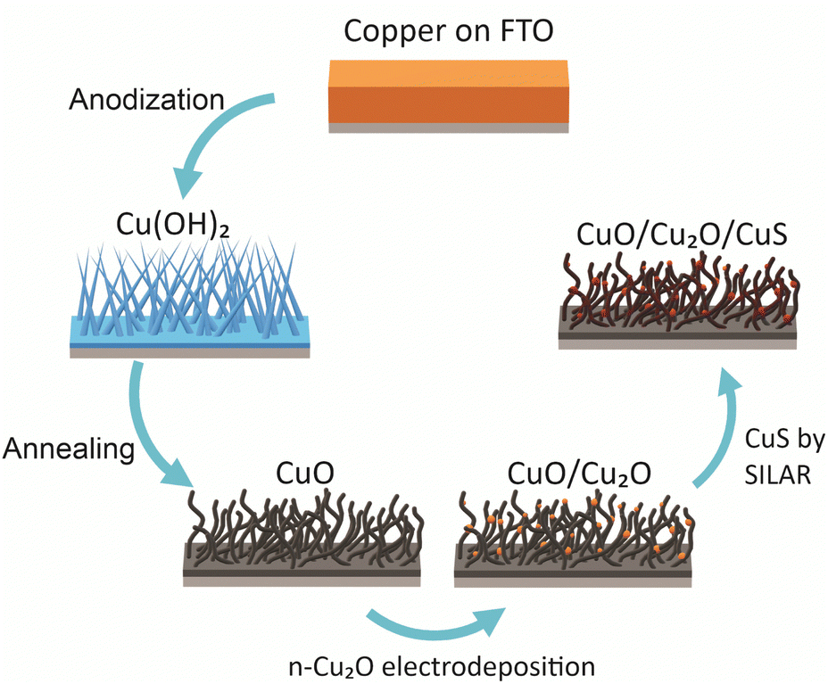 | ||
| Scheme 1 Summary of the experimental procedure to produce nanostructured films of CuO/Cu2O/CuS. | ||
Physical characterizations
Morphological characterizations were performed using scanning electron microscopy (SEM) images acquired in high resolution field emission using a FEG-SEM ZEISS SUPRATM 35. Details of the crystalline structure were investigated by X-ray diffraction (XRD) using a Rigaku – DMax2500PC with Cu Kα as a radiation source with a wavelength of 1.5406 Å. X-ray diffractograms were obtained with a scanning rate of 0.2° min−1 and a step of 0.02°. The chemical environment and oxidation state of the elements were determined by X-ray photoelectron spectroscopy (XPS) using a Scienta Omicron spectrometer, model ESCA 2SR with Al Kα (1486.7 eV) as a source of excitation. All XPS spectra were treated in the CasaXPS computer program version 2.3.17PR1.1.120. Optoelectronic characterizations were performed on a NIR-UV-VIS spectrophotometer (Varian, CARY 5G) equipped with a diffuse reflectance module.Electrochemical characterizations
A PEC cell equipped with a quartz window and a polytetrafluoroethylene body was used for the photoelectrochemical measurements. The surface area of the films exposed inside the cell was approximately 1 cm2. Photoelectrochemical measurements were performed using a potentiostat/galvanostat (Autolab, PGSTAT 302N). A LCS-100 solar simulator (Oriel, Newport) equipped with a 100 W Xe lamp, AM1.5 filter and a shutter was used as the light source. All experiments were performed using a light power density of 100 mW cm−2, calibrated with a silicon reference cell coupled to an optical power meter (Thorlabs, PM200). All photoelectrochemical experiments were carried out in N2 purged 0.5 mol L−1 Na2SO4 solution with pH adjusted to 6. A platinum spiral electrode was used as counter electrode and an Ag|AgCl|Cl− (KCl saturated) as a reference. The photoelectrocatalytic performance was evaluated considering the photocurrent produced under the illumination minus the current produced in the dark in the linear scanning voltammetry and chronoamperometry (transient photocurrent) under pulsed illumination. Electrochemical impedance (EIS) was used to determine the transfer resistance and Mott–Schottky (MS) analysis. All measurements were carried out applying 10 mV of AC perturbation. The potentials originally measured in Ag/AgCl were converted to the reversible hydrogen electrode (RHE) scale using the eqn (1): | (1) |
 is the standard potential for Ag/AgCl/KCl sat. which is 0.197 V.
Results
Anodization of metallic copper in alkaline medium followed by thermal treatment is a simple and reproducible way to obtaining nanostructured films (1D structures) of CuO. During the anodization, copper suffer electrochemical dissolution and release Cu2+ ions in solution, as showed in eqn (2). Due to the high pH of the electrolyte, the Cu2+ react quickly with the OH− anions producing Cu(OH)2, which precipitates on the substrate with a morphology similar to rods or needles of nanometric dimensions (Scheme 1), as shown in eqn (3).33,36 Also, thermal treatment in an oxygen-rich environment induces Cu(OH)2 dehydration to CuO (eqn (4)).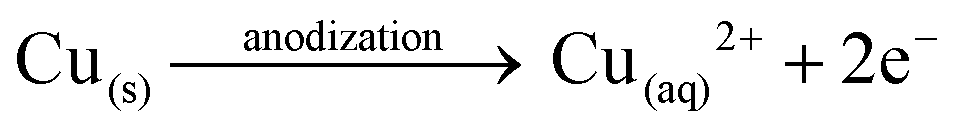 | (2) |
| Cu(aq)2+ + 2OH− → Cu(OH)2(s)↓ | (3) |
 | (4) |
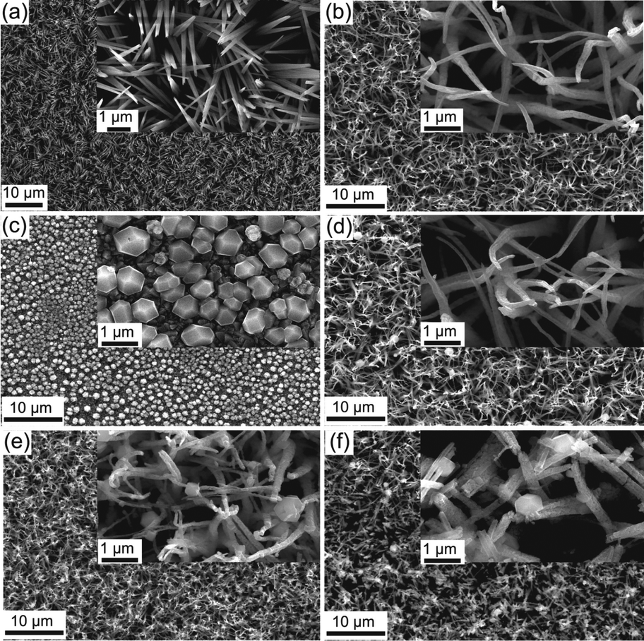 | ||
| Fig. 1 SEM surface images of (a) Cu(OH)2 nanoneedles, (b) CuO nanowires, (c) Cu2O polyhedral particles, (d) CuO/Cu2O 0 V, (e) CuO/Cu2O −0.1 V and (f) CuO/Cu2O −0.2 V. | ||
SEM images of CuO film produced by thermal treatment of the Cu(OH)2 can be seen in Fig. 1b. The thermal treatment produced morphological changes in the nanoneedles, transforming them into nanowires. These structural modifications, which can be clearly observed in the insert in Fig. 1b, come from dehydration and structural reorganization due to the thermal conversion of Cu(OH)2 into CuO. In Fig. 1c, the polyhedral Cu2O particles electrodeposited on FTO at −0.1 V can be observed, they showed good homogeneity in geometric shape and a mean diameter of 0.63 ± 0.13 μm.
SEM images of CuO/Cu2O film obtained at 0 V can be seen in Fig. 1d. The surface structures of CuO/Cu2O were like those obtained for CuO, differing only by the occurrence of a few polyhedral Cu2O particles deposited in a scattered way on the branch-like structures of CuO. Cu2O particles deposited at this potential had a diameter as large as 1.15 ± 0.28 μm. Probably, due to the low deposition potential (0 V), the Cu2O particles slowly nucleated and concentrated in a few regions of the CuO nanowires, which allowed the deposition of large Cu2O particles. The image inserted in Fig. 1d shows that the CuO nanowires remained almost unchanged after the Cu2O particle deposition process.
The CuO/Cu2O film obtained at −0.1 V (Fig. 1e) presented nanowire-like structures with more Cu2O particles dispersed over these structures compared to the CuO/Cu2O 0 V film. In this film, the Cu2O particles had an average diameter of 0.43 ± 0.13 μm, much smaller than those observed in CuO/Cu2O 0 V. It is noteworthy that although there was a greater dispersion of Cu2O structures, the CuO nanowires were apparently more twisted and broken compared to the unmodified CuO film.
The SEM images for the CuO/Cu2O film obtained at −0.2 V can be seen in Fig. 1f. As in the CuO/Cu2O −0.1 V film, the Cu2O particles were dispersed and had a mean diameter of 0.49 ± 0.12 μm. Also, clusters of Cu2O particles were observed. Furthermore, CuO nanowires were even more defective compared to CuO/Cu2O −0.1 V. This fact can lead to a substantial decrease in the active area of the film and the loss of ohmic contact between the CuO wires and the substrate, which should negatively affect the photoelectrochemical HER efficiency.
Morphological characterizations were also carried out for the CuO/Cu2O −0.1 V film modified with the CuS cocatalyst. CuS was chosen due to its ease of synthesis and good results that have already been demonstrated for similar systems to those produced in this work.22,27 Fig. S1a (ESI†) shows surface image by SEM of CuO/Cu2O/CuS obtained after 6 cycles of SILAR. No morphological significant differences of CuO/Cu2O/CuS compared to CuO/Cu2O −0.1 V was noticed. However, the elemental mapping by EDX showed in Fig. S1b–d (ESI†), show that Cu, O and S were homogeneously dispersed on the surface of the CuO/Cu2O/CuS film with an estimated atomic percentage of 44.6%, 52.9% and 2.5%, respectively. Furthermore, SEM cross-section imaging of CuO/Cu2O/CuS (Fig. S2a, ESI†) showed the CuO nanowires were quasi-vertically randomly aligned with a length of approximately 9.6 μm. Also, elemental mapping by EDX was performed for the cross section (Fig. S2b–d, ESI†) and showed that Cu, O and S were homogeneously distributed under the sample.
The crystalline structure was evaluated by X-ray diffraction and the diffractograms can be visualized in Fig. 2a. The pattern obtained for the anodized film (Cu(OH)2), exhibited the phases of Cu(OH)2 with their main peaks at 16.7°, 23.8°, 34° and 53.2° (ICSD #68459, orthorhombic system),37 Metallic Cu with a strong peak at 43.4° (ICSD #43493, cubic system),38 Cu2O (ICSD #63281, cubic system)39 with major peaks at 36.4° and 42.3° and SnO2 from the FTO substrate (ICSD no. 16635, tetragonal system).40 The presence of metallic copper is due to the incomplete conversion of copper to Cu(OH)2. The presence of Cu2O shows that Cu(OH)2 is not the only oxidized copper species formed during the anodizing process. The diffractogram for the film obtained after the heat treatment (CuO) showed only CuO peaks (ICSD no. 87123, monoclinic system)41 at 32.6°, 35.5° and 38.8°. The diffractogram peaks were relatively wide indicating a low crystallinity of CuO. Peaks of SnO2 phase were also identified. The presence of only CuO and SnO2 phases points to a complete thermal conversion of the Cu(OH)2, Cu and Cu2O phases. To prove that the polyhedral particles shown in Fig. 1c were from Cu2O, a diffractogram was obtained for the Cu2O film deposited at −0.1 V on FTO. Only Cu2O and SnO2 were identified, confirming that the polyhedral particles were pure phase of Cu2O. Furthermore, the Cu2O peaks were narrow and intense, indicating good crystallinity. The pattern for the CuO/Cu2O −0.1 film (CuO/Cu2O) showed peaks related to the CuO, Cu2O and SnO2 phases, no copper hydroxide or metallic copper phases were observed. Finally, the diffractogram for the CuO/Cu2O/CuS film exhibited phases of CuO, Cu2O and SnO2, but no peaks of CuS phase was identified. The non-appearance of CuS is due to its low concentration in the CuO/Cu2O/CuS film, since only 2.5% (in atomic percentage) of sulphur was detected in the EDX measurement.
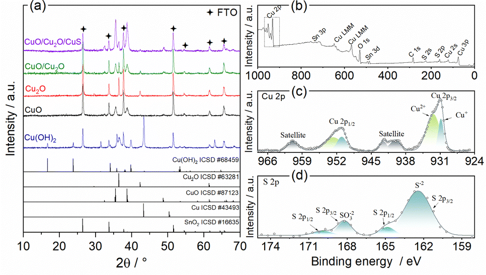 | ||
| Fig. 2 (a) XRD pattens of Cu(OH)2, CuO, Cu2O, CuO/Cu2O, and CuO/Cu2O/CuS samples. XPS spectra of CuO/Cu2O/CuS sample: (b) survey, (c) high resolution Cu 2p and (d) high resolution S 2p. | ||
The chemical environment of the elements in the CuO/Cu2O/CuS film was analyzed by X-ray photoelectron spectroscopy (XPS), the exploratory spectrum (survey) is shown in Fig. 2b. As can be seen, all constituent elements such as copper, oxygen and sulfur were identified. In addition, a peak of adventitious carbon was noted, which was attributed to the presence of adsorbed CO2 and/or organic contaminants. The high resolution spectrum in the Cu 2p region is shown in Fig. 2c. Signals with binding energy values of approximately 931.0 eV and 951.2 eV were assigned to Cu 2p3/2 and Cu 2p1/2, respectively.42,43 The band assigned to Cu 2p3/2 was deconvolved into two other bands related to Cu+ (930.8 eV) and Cu2+ (932.5 eV).42,43 The presence of Cu+ and Cu2+ signals in the XPS spectrum corroborates the XRD measurements that show the presence of CuO and Cu2O in this sample. From the Cu 2p3/2 band it was determined that the atomic percentage of the Cu2+ and Cu+ species was 72% and 28%, respectively. The high resolution XPS spectrum in the S 2p region is shown in Fig. 2d. The band with binding energy at 163 eV was attributed to the S2−, this signal was deconvolved into two other signals related to S 2p3/2 (162.3 eV) and S 2p1/2 (164.7 eV).22,27 The presence of S2− confirms the formation of CuS by the SILAR method on the CuO/Cu2O film. In addition to the S2− signal, another band located between 165.4 eV and 170.6 eV was attributed to SO32−.44 This band was also deconvolved into S 2p3/2 (168.1 eV) and S 2p1/2 (169.8 eV). The appearance of SO32− may be related to the presence of Na2SO3 that formed during the CuS deposition process.44 Finally, the atomic percentages of Cu, O and S on the surface of the CuO/Cu2O/CuS were determined to 29.9%, 52.9% and 17.3%, respectively. This demonstrate that the surface of CuO/Cu2O/CuS presented a higher concentration of S when compared to material bulk as observed by EDX analyses.
The optoelectronic properties of CuO, Cu2O and CuO/Cu2O films were examined by diffuse reflectance spectroscopy in the UV-vis region (DRS). The values of the band gap energies (Eg) were determined from the Tauc relation and the Kubelka–Munk radiative transfer model.45,46
The DRS and Tauc graphs for CuO, Cu2O and CuO/Cu2O can be seen in Fig. 3. The DRS spectrum for CuO (Fig. 3a) shows, by the decay of the reflectance value, that the absorption of light in this film starts close to 900 nm and remains throughout the entire region of the visible spectrum (from 750 nm to ∼400 nm). The Tauc plot constructed with the DRS data (insert in Fig. 3a) displays an Eg of 1.62 eV for CuO that is close to the values observed in the literature.47,48 According to Fig. 3b, the Cu2O film showed an onset of absorption at approximately 650 nm. According to the Tauc graph (insert in Fig. 3b), the Eg value determined for Cu2O was 2.02 eV, this value agrees with the values observed in the literature.18,49
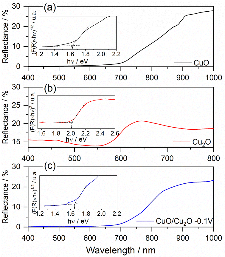 | ||
| Fig. 3 Diffuse reflectance spectrum and Tauc plot of (a) CuO, (b) Cu2O and (c) CuO/Cu2O −0.1 V films. | ||
The DRS spectrum and Tauc plot for the CuO/Cu2O film can be seen in Fig. 3c. As can be seen, CuO/Cu2O showed a reflectance profile like that for CuO with absorption onset close to 900 nm and an Eg of 1.65 eV, which is only slightly higher than that observed for CuO. The presence of Cu2O must have influenced the band gap increasing.
The photoelectrochemical activities of CuO and CuO/Cu2O films were evaluated for the water splitting. The photocurrent density was considered the main factor to evaluate the quality of the photocathodes and it was determined by the subtraction of the current density measured under illumination and the current density measured in the absence of light. The linear sweep voltammogram (LSV) under pulsed light for the Cu2O film obtained on FTO can be seen in Fig. 4a. The photocurrent pulses generated in the presence of light for potentials more positive than 0.3 VRHE were anodic, indicating a behavior of an n-type semiconductor. In addition, the intense current spikes were attributed to the recombination mechanism of the photogenerated charge carriers. The Fig. 4b presents the LSVs obtained under pulsed light for CuO and CuO/Cu2O films obtained at different Cu2O deposition potentials. The charge density for the Cu2O deposition on CuO was fixed in −0.1 C cm−2. Charge densities of −0.2 and −0.3 C cm−2 also was tested, but these films exhibited a decline in activity as showed in Fig. S3 (ESI†). All films of CuO/Cu2O had negative photocurrent density, indicating a p-type conductivity. Thus, the electrons photogenerated by the action of light and the applied potential were conducted to the electrode/electrolyte interface, leading to the photoelectrochemical reduction of water and generation of H2. The occurrence of current in the unilluminated region of the LSVs at potentials more negative than 0.1 VRHE is related to the electrochemical reduction of copper oxides to metallic copper.24
 | ||
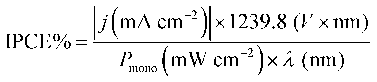
| Fig. 4 Linear sweep voltammograms at 5 mV s−1 under 1.5G pulsed illumination (100 mW cm−2) of (a) Cu2O and (b) CuO, CuO/Cu2O 0 V, CuO/Cu2O −0.1 V and CuO/Cu2O −0.2 V in 0.5 mol L−1 Na2SO4 solution (pH 6). (c) Mean and standard deviation of the photocurrent density values obtained at 0.1 VRHE. (d) HC-ABPE efficiency for CuO and CuO/Cu2O films. | ||
The average photocurrent densities and standard deviations obtained at 0.1 VRHE for all films can be seen in Fig. 4c. The photocurrent density obtained for bare CuO film was −1.43 ± 0.01 mA cm−2. This value is within the expected range, as shown by recent works reporting CuO nanostructures as photocathode for water splitting.13,25 The films CuO/Cu2O 0 V and CuO/Cu2O −0.2 V presented photocurrent densities of 1.38 ± 0.27 and 1.50 ± 0.02 mA cm−2, respectively. These films did not show a significant increase in photoelectrochemical activity compared to bare CuO. In the case of CuO/Cu2O 0 V, the occurrence of few dispersed particles under the CuO wires, as showed in Fig. 1d, must have been the cause of the imperceptible improvement in activity. About CuO/Cu2O −0.2 V, the large amount of twisted and broken CuO structures, caused by the Cu2O deposition process, as observed in Fig. 1f, may have negatively influenced the photoelectrocatalytic activity for this film.
The CuO/Cu2O −0.1 V film presented the highest photocurrent (−1.62 ± 0.31 mA cm−2) and, therefore, the best photoelectrochemical activity. As shown in Fig. 1e, the Cu2O particles in this film were well dispersed and the CuO structures were not as twisted and broken as in CuO/Cu2O −0.2 V. Therefore, the balance between the amount of Cu2O particles and the maintenance of the morphology of the CuO structures must be the main reason for the best activity of CuO/Cu2O −0.1 V. The best activity of CuO/Cu2O −0.1 V was also confirmed by the half-cell applied bias photon-to-current efficiency (HC-ABPE). The HC-ABPE is one of the simplest ways to measure the efficiency of using the incident light in the photoelectrochemical conversion by the photoelectrode and can be calculated by eqn (5):50
 | (5) |
As a way of accelerating the electronic transfer at the electrode/solution interface and thus promoting an increase in the photoelectrochemical activity, CuS as a cocatalyst was deposited by 6 SILAR cycles on the CuO/Cu2O −0.1 V film. Other numbers of SILAR cycles were tested, but the best film was obtained with 6 cycles, as shown in Fig. S4 (ESI†).
The LSVs for bare CuO, CuO/Cu2O −0.1 V and CuO/Cu2O/CuS films can be seen in Fig. 5a. It be seen the photoelectrode modified with CuS showed the highest photocurrent density (−2.74 mA cm−2 at 0 VRHE) among the tested films, indicating its better photoelectrocatalytic. The incident photon-to-current efficiency (IPCE) is an important parameter to evaluate the conversion efficiency of the incident photon flux to photocurrent, as a function of the wavelength of the light source. The IPCE can be calculated from eqn (6):51
 | (6) |
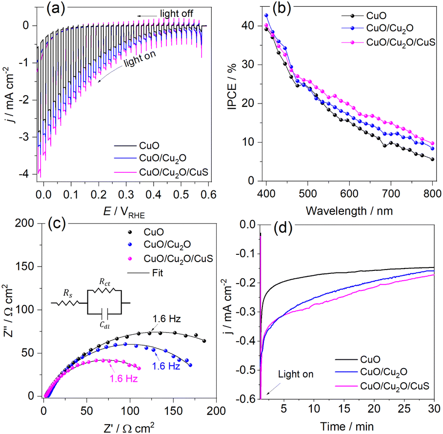 | ||
| Fig. 5 (a) Linear sweep voltammograms at 5 mV s−1, (b) IPCE efficiency at 0.2 VRHE and (c) Nyquist plots at 0.2 VRHE for CuO, CuO/Cu2O −0.1 V and CuO/Cu2O/CuS films. (d) Stability test (photocurrent transient) at 0.35 VERH for CuO and CuO/Cu2O/CuS films. Experiments carried out in 0.5 mol L−1 Na2SO4 solution (pH 6) under 1.5G (100 mW cm−2) illumination. | ||
Electrochemical impedance spectroscopy was carried out to bare CuO, CuO/Cu2O and CuO/Cu2O/CuS films at 0.2 VRHE under visible light to obtaining details about the charge transfer resistance. Fig. 5c shows the Nyquist plot fitted with a Randles equivalent circuit (insert in Fig. 5c). The Randles circuit is constituted of the electrolyte resistance (Rs) in series with the doble layer capacitance (Cdl) and charge transfer resistance (Rct), Table S1 (ESI†) present the values found for Rs, Cdl and Rct. As expected, CuO/Cu2O/CuS exhibited the lowest Rct (13247 Ω cm−2) that confirms the fast charge transfer in the interface photoelectrode/electrolyte and its greater photoelectrocatalytic activity. Furthermore, CuO/Cu2O showed a lower Rct (187.80 Ω cm−2) compared to bare CuO (248.15 Ω cm−2), which agrees with the curves of LSVs and IPCE efficiency. As Rs and Cdl are not involved in the charge transfer process, these parameters were similar for all photoelectrodes.
Transient photocurrent measurements (chronoamperometry) were performed to evaluate the stability of CuO, CuO/Cu2O and CuO/Cu2O/CuS films. In this test, the photoelectrodes were polarized at 0.35 VRHE under light AM 1.5G and 100 mW cm−2. As shown in Fig. 5d, bare CuO exhibited considerable deactivation at the beginning of the experiment and then the photocurrent remained almost constant until the end. The loss of activity of CuO is mainly due to the electrochemical and photoelectrochemical reduction of CuO to Cu2O, which occurs in potential more negative than 0.4 VRHE.52 Although CuO/Cu2O and CuO/Cu2O/CuS showed a higher photocurrent at the beginning of the experiment, as well as CuO, this photoelectrodes also showed deactivation during the test. The CuO/Cu2O/CuS presented a higher charge transfer of interface photoelectrode/electrolyte provided by the CuS cocatalyst, which enables a faster flow of the photogenerated electrons, this fact does not prevent that part of the photogenerated electrons act in the photocorrosion of CuO and Cu2O. The SEM surface images and EDX mapping obtained before and after the stability for bare CuO (Fig. S5a and b, respectively, ESI†) showed that the nanowires of CuO undergo morphological changes caused by the photocorrosion. It is important to emphasize that the Cu/O ratio changes from 0.89 to 1.83 after the stability test, confirming the photoreduction of CuO to Cu2O. SEM image and EDX elemental mapping were also carried out to CuO/Cu2O/CuS before and after the stability test as showed in Fig. S5c and d (ESI†), respectively. CuO/Cu2O/CuS also presented morphological changes, but these alterations were less evident than those for bare CuO. For this film the Cu/O ratio changes from 0.83 to 1.42 after the stability test, indicating that less CuO was converted to Cu2O. It is noteworthy that the amount of S changes from 2.5% to 0.7% after the stability test, showing that CuS also suffered photocorrosion.
To understand the behavior of the CuO/Cu2O junction and why this material has a better photoelectrocatalytic activity for HER compared to CuO, the flat band potential (Efb), the valence band maximum (VBM) and the conduction band minimum (CBM) for FTO/CuO and FTO/Cu2O films were determined. Due to the nanometric structures (nanowires) of CuO the determination of the capacitance of the space charge region and Efb by Mott–Schottky (M–S) is improper, thus chopped illumination (CI) was the technique used to determine the Efb.53 To determine the Efb by CI, a LSV with a slow scan rate under pulsed illumination is performed in potentials where the conductivity transition occurs, the Efb is considered equal to transition point. This technique was studied by Hankin, A. et al.54 and compared to other techniques for the determination of the flat band potential, this is among those that exhibited better accuracy. As can be seen in Fig. 6a, the transition point (Efb) for CuO was 1.1 VRHE that agrees with the literature.55 As CuO is a p-type semiconductor the Efb can be considered very close to VBM.24 The CI was also used to determine the Efb of the FTO/Cu2O film (Fig. 6b). The transition point between n-type conduction and p-type conduction was at −0.22 VRHE. As Cu2O is an n-type semiconductor, Efb is expected to be very close to CBM. The Cu2O film had a flat morphology (Fig. 1c) and to confirm the Efb, M–S analyses was performed to this film. As showed in the graph inserted in Fig. 6b, the Efb value for Cu2O determined by M–S was −0.2 VRHE, value close that determined by CI. Considering the Efb of CuO and Cu2O, the VBM and CBM for both materials were determined using the eqn (7).56
 | (7) |
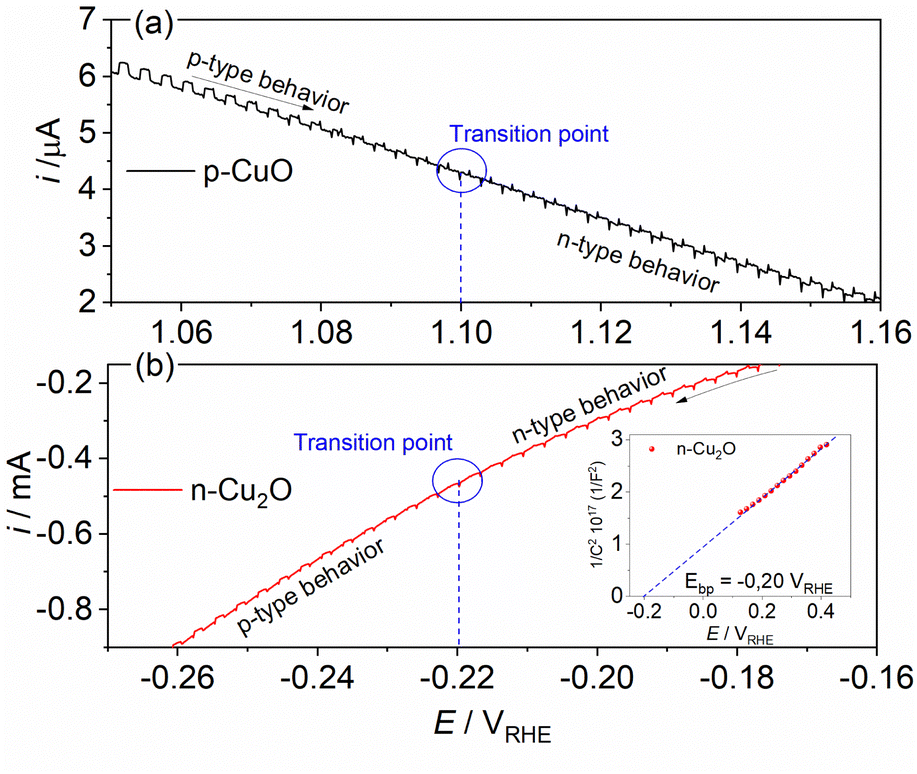 | ||
| Fig. 6 Linear voltammogram under pulsed illumination (5 mV s−1 and pulse frequency 1 Hz) in the conductivity transition region for (a) p-CuO and (b) n-Cu2O in 0.5 mol L−1 Na2SO4 solution (pH 6). | ||
| Sample | E g (eV) | E fb (V) | VBM (eV) | CBM (eV) |
|---|---|---|---|---|
| CuO | 1.62 | 1.10 | −5.54 | −3.92 |
| Cu2O | 2.02 | −0.22 | −6.24 | −4.22 |
Assuming that the junction between the two materials do not significantly change the individual VBM and CBM values, a band diagram for the CuO/Cu2O/CuS film was drawn as showed in Fig. 7. The VBM and CBM for p-CuO and n-Cu2O suggest the formation of a type II p–n heterojunction, which implies a more efficient separation of charge carriers and a consequent reduction in recombination. Then, when illuminated with visible light, both p-CuO and n-Cu2O can absorb photons. This excites electrons in their valence bands, leading them to the conduction bands, creating photogenerated electrons and holes. At the interface between p-CuO and n-Cu2O, a built-in potential arises due to the difference in their electron affinities. This creates a depletion region where majority carriers (holes in p-CuO and electrons in n-Cu2O) are depleted. The depletion region promotes an electric field directed from p-CuO to n-Cu2O. Photogenerated electrons in the conduction band of both p-CuO and n-Cu2O experience opposing forces.31 However, due to the electric field, electrons in CuO are driven towards the n-Cu2O side where the conduction band has a lower energy level. In addition, the potential cascade formed between the bands of CuO and Cu2O helps the flow of photogenerated charge carriers. On the other hand, the photogenerated holes in the valence band of CuO are driven towards the FTO substrate and trough the circuit. This directional movement leads to the accumulation of photogenerated electrons in the conduction band of n-Cu2O. So, the electrons in the n-Cu2O conduction band can then migrate to CuS cocatalyst where they can participate in the hydrogen evolution reaction (HER). For this reason, the CuO/Cu2O heterojunction showed a better activity compared to bare CuO. The action of CuS as a cocatalyst had already been described in the literature. According to Dubale et al.,22 part of the electrons photogenerated from the valence bands of CuO and Cu2O are sequestered by CuS, which partially converts to Cu2S, leading to the production of a CuS/Cu2S cluster. Thus, the formed cluster acts as an active site for HER and accelerate the electron transfer.
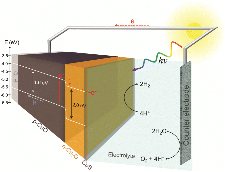 | ||
| Fig. 7 Schematic band diagram of FTO/CuO/Cu2O/CuS for the PEC water splitting. | ||
Conclusions
Herein, p-CuO nanostructure films were functionalized with n-Cu2O and CuS. The n-Cu2O has adequate conduction and valence bands for a p–n heterojunction with CuO, which promoted the reduction of recombination and increased the lifetime of charge carriers. To further improve the activity of the CuO/Cu2O film, this material was modified with CuS by the SILAR method. The best CuO/Cu2O/CuS film showed a photocurrent of −2.74 mA cm−2, while pure CuO showed only −2.11 mA cm−2 at 0 VRHE. In addition, the incident-photon-to-current efficiency (IPCE) was 30% higher for CuO/Cu2O/CuS compared to pure CuO at 580 nm. In summary, the type II p–n heterojunction formed between CuO and Cu2O provided better charge separation and CuS catalyzed the hydrogen evolution reaction (HER).Author contributions
Hugo L. S. Santos: experimental part, investigation, writing and editing. Lucia H. Mascaro: supervision, funding, review, and editing.Data availability
All data, figures, tables of the work are in the google drive repository – https://drive.google.com/drive/home provided by the Federal University of São Carlos. The files are also stored in a dropbox folder shared between the authors that can be consulted when requested.Conflicts of interest
There are no conflicts to declare.Acknowledgements
The authors thank the Laboratory of Structural Characterization (LCE/DEMa/UFSCar) for the general facilities and Professor Valmor Mastelaro for the XPS measurements. The authors also thank the São Paulo Research Foundation (FAPESP) for the financial assistance to the project and the fellowship granted (#2019/26860-2, #2017/11986-5 and #2013/07296-2), Financier of Studies and Projects (FINEP grant # 01.22.0179.00) and the National Council for Scientific and Technological Development (CNPq, grant #311769/2022-5, # 406156/2022-0). The Shell and the strategic importance of the support given by ANP (Brazil's National Oil, Natural Gas and Biofuels Agency) through the R&D levy regulation.References
- M. Balat, Energy Sources, 2009, 31, 1242–1255 CrossRef CAS.
- B. N. Nunes, L. F. Paula, Í. A. Costa, A. E. H. Machado, L. G. Paterno and A. O. T. Patrocinio, J. Photochem. Photobiol., C, 2017, 32, 1–20 CrossRef CAS.
- Y. W. Phuan, W. J. Ong, M. N. Chong and J. D. Ocon, J. Photochem. Photobiol., C, 2017, 33, 54–82 CrossRef CAS.
- Y. Liu, Y. X. Yu and W. De Zhang, Electrochim. Acta, 2012, 59, 121–127 CrossRef.
- M. Moriya, T. Minegishi, H. Kumagai, M. Katayama, J. Kubota and K. Domen, J. Am. Chem. Soc., 2013, 135, 3733–3735 CrossRef CAS PubMed.
- M. Li, R. Zhao, Y. Su, J. Hu, Z. Yang and Y. Zhang, Adv. Mater. Interfaces, 2016, 3, 1–10 Search PubMed.
- G. Wang, H. Wang, Y. Ling, Y. Tang, X. Yang, R. C. Fitzmorris, C. Wang, J. Z. Zhang and Y. Li, Nano Lett., 2011, 11, 3026–3033 CrossRef CAS PubMed.
- G. Zheng, J. Wang, H. Liu, V. Murugadoss, G. Zu, H. Che, C. Lai, H. Li, T. Ding, Q. Gao and Z. Guo, Nanoscale, 2019, 11, 18968–18994 RSC.
- D. Coelho, J. P. R. S. Gaudêncio, S. A. Carminati, F. W. P. Ribeiro, A. F. Nogueira and L. H. Mascaro, Chem. Eng. J., 2020, 399, 125836 CrossRef CAS.
- M. G. Lee and H. W. Jang, J. Korean Ceram. Soc., 2016, 53, 400–405 CrossRef CAS.
- J. N. Nian, C. C. Hu and H. Teng, Int. J. Hydrogen Energy, 2008, 33, 2897–2903 CrossRef CAS.
- Z. Zhang and P. Wang, J. Mater. Chem., 2012, 22, 2456–2464 RSC.
- J. Li, X. Jin, R. Li, Y. Zhao, X. Wang, X. Liu and H. Jiao, Appl. Catal., B, 2019, 240, 1–8 CrossRef CAS.
- S. Masudy-Panah, Y. J. K. Eugene, N. D. Khiavi, R. Katal and X. Gong, J. Mater. Chem. A, 2018, 6, 11951–11965 RSC.
- X. Guo, P. Diao, D. Xu, S. Huang, Y. Yang, T. Jin, Q. Wu, M. Xiang and M. Zhang, Int. J. Hydrogen Energy, 2014, 39, 7686–7696 CrossRef CAS.
- F. P. Koffyberg and F. A. Benko, J. Appl. Phys., 1982, 53, 1173–1177 CrossRef CAS.
- H. L. S. Santos, P. G. Corradini, M. A. S. Andrade Jr and L. H. Mascaro, J. Solid State Electrochem., 2020, 24, 1899–1908 CrossRef CAS.
- T. Jiang, T. Xie, W. Yang, H. Fan and D. Wang, J. Colloid Interface Sci., 2013, 405, 242–248 CrossRef CAS PubMed.
- Y. K. Hsu, C. H. Yu, Y. C. Chen and Y. G. Lin, Electrochim. Acta, 2013, 105, 62–68 CrossRef CAS.
- Y. Yang, D. Xu, Q. Wu and P. Diao, Sci. Rep., 2016, 6, 1–13 CrossRef CAS.
- C. Ma, Z. Liu, Q. Cai, C. Han and Z. Tong, Inorg. Chem. Front., 2018, 5, 2571–2578 RSC.
- A. A. Dubale, A. G. Tamirat, H. M. Chen, T. A. Berhe, C. J. Pan, W. N. Su and B. J. Hwang, J. Mater. Chem. A, 2016, 4, 2205–2216 RSC.
- D. Jeong, W. Jo, J. Jeong, T. Kim, S. Han, M. K. Son and H. Jung, RSC Adv., 2022, 12, 2632–2640 RSC.
- W. Septina, R. R. Prabhakar, R. Wick, T. Moehl and S. D. Tilley, Chem. Mater., 2017, 29, 1735–1743 CrossRef CAS.
- C.-Y. Lin, Y.-H. Lai, D. Mersch and E. Reisner, Chem. Sci., 2012, 3, 3482 RSC.
- P. Wang, Z. Liu, D. Chen, S. Zhang, G. Fang, C. Han, Z. Cheng and Z. Tong, Catal. Lett., 2021, 151, 1976–1983 CrossRef CAS.
- G. Panzeri, M. Cristina, M. S. Jagadeesh, G. Bussetti and L. Magagnin, Sci. Rep., 2020, 10, 1–10 CrossRef PubMed.
- P. Wang, Z. Liu, C. Han, X. Ma, Z. Tong and B. Tan, J. Nanopart. Res., 2021, 23, 268 CrossRef CAS.
- T. Wang, Y. Wei, X. Chang, C. Li, A. Li, S. Liu, J. Zhang and J. Gong, Appl. Catal., B, 2018, 226, 31–37 CrossRef CAS.
- R. P. Wijesundera, Semicond. Sci. Technol., 2010, 25, 5 CrossRef.
- R. P. Wijesundera, M. Hidaka, K. Koga, J. Y. Hoi and N. E. Sung, Ceram.-Silik., 2010, 54, 19–25 CAS.
- W. Shi, X. Zhang, S. Li, B. Zhang, M. Wang and Y. Shen, Appl. Surf. Sci., 2015, 358, 404–411 CrossRef CAS.
- J. Luo, L. Steier, M. K. Son, M. Schreier, M. T. Mayer and M. Grätzel, Nano Lett., 2016, 16, 1848–1857 CrossRef CAS PubMed.
- A. C. Salomao, M. dos Santos Araujo, H. L. S. dos Santos, M. Medina, L. H. Mascaro and M. A. S. Andrade Junior, ChemSusChem, 2021, 14, 4671–4679 CrossRef CAS PubMed.
- J. C. Ballesteros, E. Chaînet, P. Ozil, G. Trejo and Y. Meas, J. Electroanal. Chem., 2010, 645, 94–102 CrossRef CAS.
- Z. Zhang, R. Dua, L. Zhang, H. Zhu, H. Zhang and P. Wang, ACS Nano, 2013, 7, 1709–1717 CrossRef CAS PubMed.
- H. R. Oswald, A. Reller, H. W. Schmalle and E. Dubler, Acta Crystallogr., Sect. C: Cryst. Struct. Commun., 1990, 46, 2279–2284 CrossRef.
- H. M. Otte, J. Appl. Phys., 1961, 32, 1536–1546 CrossRef CAS.
- R. Restori and D. Schwarzenbach, Acta Crystallogr., Sect. B: Struct. Sci., 1986, 42, 201–208 CrossRef.
- W. H. Baur, Acta Crystallogr., 1956, 9, 515–520 CrossRef CAS.
- V. Massarotti, D. Capsoni, M. Bini, A. Altomare and A. G. G. Moliterni, Z. Kristallogr. - Cryst. Mater., 1998, 213, 259–265 CrossRef CAS.
- B. Sen, E. Kuyuldar, A. Şavk, H. Calimli, S. Duman and F. Sen, Int. J. Hydrogen Energy, 2019, 44, 10744–10751 CrossRef CAS.
- M. C. Biesinger, Surf. Interface Anal., 2017, 49, 1325–1334 CrossRef CAS.
- S. Murugan, S. Niesen, J. Kappler, K. Küster, U. Starke and M. R. Buchmeiser, Batteries Supercaps, 2021, 4, 1636–1646 CrossRef CAS.
- P. Makuła, M. Pacia and W. Macyk, J. Phys. Chem. Lett., 2018, 9, 6814–6817 CrossRef PubMed.
- F. W. D. S. Lucas, A. R. F. Lima and L. H. Mascaro, RSC Adv., 2015, 5, 18295–18300 RSC.
- X. Guo, P. Diao, D. Xu, S. Huang, Y. Yang, T. Jin, Q. Wu, M. Xiang and M. Zhang, Int. J. Hydrogen Energy, 2014, 39, 7686–7696 CrossRef CAS.
- C. Y. Chiang, Y. Shin and S. Ehrman, Appl. Energy, 2016, 164, 1039–1042 CrossRef CAS.
- S. R. Meher, A. Lakshmanan, D. Gupta and Z. C. Alex, Mater. Today Commun., 2021, 26, 102015 CrossRef CAS.
- J. Ji, P. Sang and J. H. Kim, Ceram. Int., 2021, 47, 26260–26270 CrossRef CAS.
- D. S. Ellis, Y. Piekner, D. A. Grave, P. Schnell and A. Rothschild, Front. Energy Res., 2022, 9, 1–14 Search PubMed.
- H. Xing, E. Lei, Z. Guo, D. Zhao, X. Li and Z. Liu, Inorg. Chem. Front., 2019, 6, 2488–2499 RSC.
- K. Sivula, ACS Energy Lett., 2021, 6, 2549–2551 CrossRef CAS.
- A. Hankin, F. E. Bedoya-Lora, J. C. Alexander, A. Regoutz and G. H. Kelsall, J. Mater. Chem. A, 2019, 7, 26162–26176 RSC.
- S. A. Monny, L. Zhang, Z. Wang, B. Luo, M. Konarova, A. Du and L. Wang, J. Mater. Chem. A, 2020, 8, 2498–2504 RSC.
- A. E. B. Lima, M. Assis, A. L. S. Resende, H. L. S. Santos, L. H. Mascaro, E. Longo, R. S. Santos, L. S. Cavalcante and G. E. Luz, J. Solid State Electrochem., 2022, 26, 997–1011 CrossRef CAS.
Footnote |
| † Electronic supplementary information (ESI) available. See DOI: https://doi.org/10.1039/d4ma00343h |
| This journal is © The Royal Society of Chemistry 2024 |