DOI:
10.1039/D4MA00298A
(Paper)
Mater. Adv., 2024,
5, 4832-4847
Growth of a CuSbSe2 single crystal by the Bridgman technique and its utility as a photodetector and thermoelectric material
Received
21st March 2024
, Accepted 16th April 2024
First published on 30th April 2024
Abstract
Looking at the literature survey, this seems to be the first report on growth of a copper antimony diselenide (CuSbSe2) single crystal with a 5.8 cm length and 1.0 cm diameter by the vertical Bridgman technique. The validation of the orthorhombic crystal structure of CuSbSe2 is obtained through outcomes of the powder X-ray diffraction pattern. The stoichiometry of the grown crystal is corroborated via energy dispersive X-ray analysis, whereas field emission scanning electron microscopy displays a growth pattern comprising both a smooth surface and layer growth. The confirmation of the crystalline nature of the crystal is provided by the distinctive spot patterns observed in the selected area electron diffraction pattern. The observed d value closely corresponds to the d value of the prominent (112) plane of orthorhombic CuSbSe2. The Raman spectra depicted two prominent peaks at 194.74 cm−1 and 232.32 cm−1 corresponding to the Ag vibrational mode and also showed the orthorhombic phase of CuSbSe2. Optical reflectance spectroscopy substantiated that the CuSbSe2 single crystal possesses a direct bandgap of 1.3 eV, rendering it a suitable candidate for potential solar cell applications. Throughout the temperature range from 310 K to 586 K, the Seebeck coefficient maintains a positive value, conclusively affirming the p-type semiconducting nature of the sample. Remarkably, zT (figure of merit) attains a value of approximately 0.976 at 543 K, a result that competes effectively with values reported for other grown crystals. The thermogravimetric (TG) curve indicated weight gain along with weight loss, which is also confirmed by the differential thermogravimetric analysis (DTG) curve at different heating rates of 5, 10, 15 and 20 K min−1. Furthermore, the I–V characteristics of the CuSbSe2 single crystal photodetector are recorded at room temperature at varying bias voltages and a light intensity of 50 mW cm−2. Pulse photoresponse is recorded for the parallel to planar configuration, and from I–V characteristics some important parameters such as photocurrent, sensitivity, responsivity, detectivity, rise time and decay time are determined. At room temperature, employing a bias voltage of 500 mV along with a light intensity of 50 mW cm−2 led to responsivity and detectivity values of 52.664 mA W−1 and 2.317 × 10⁹ Jones for the parallel to planar configuration.
1. Introduction
The escalating worldwide need for energy and the depleting reserves of fossil fuels have spurred swift and imperative investigations into substitute energy technologies.1,2 The pursuit of abundant and sustainable sources of energy and fuel stands as a pivotal challenge in today's era of global expansion.3,4 As the world faces mounting challenges related to the energy crisis, there is an increasing demand for solar energy production and the development of suitable materials for harnessing this abundant resource. The need for cost-effective and efficient photovoltaic materials has sparked fresh investigations into the synthesis of metal chalcogenides. Consequently, there is a substantial requirement for thorough exploration aimed at discovering various materials, enabling the identification of more cost-effective and easily accessible substances for the advancement of solar cell technology.5 In recent times, researchers have taken a keen interest in the practical applications of copper based chalcogenide semiconductor materials such as CuIn(S/Se)2, Cu(In,Ga)(S/Se), and Cu2ZnSn(S/Se).6,7 This focus has arisen due to the favourable attributes of these chalcogenide materials, including their environmentally benign components, abundant presence in the Earth's crust, simple manufacturing processes, and affordability. Over the past few years, the spotlight has increasingly turned towards thermoelectric (TE) materials,8,9 which possess the unique capability to directly transform surplus heat into usable electrical energy.10 These materials are a subject of interest because of their compact size, dependability, and eco-friendliness and the absence of noise and vibrations and are capable of functioning across a broad spectrum of temperatures while exhibiting a prolonged operational lifespan.11 The approach of converting heat into electricity has emerged as a promising means of sustainable power generation, aiming to mitigate the escalating energy challenges and ecological imbalances. Thermoelectric devices offer a promising solution to overcome the constraints of traditional energy sources, providing reliability, portability, and affordability. The process of thermoelectric energy conversion presents a unique opportunity to harness widely available waste heat and offers an economically viable method to convert solar energy into electrical power. However, for a material to possess optimal thermoelectric qualities, it must exhibit good efficiency, which is determined by the figure of merit zT.12 This value is derived from the equation S2σT/κ, where ‘S’ represents the Seebeck coefficient, ‘σ’ denotes the electrical conductivity, and ‘κ’ signifies the thermal conductivity. It is apparent that achieving a substantial power factor (S2σ) and minimizing κ are necessary for exceptional thermoelectric materials.13 However, the interconnected nature of these parameters (S, σ and κ) presents a challenge when striving to enhance the performance of high efficiency thermoelectric materials.14
Among the assortment of copper based chalcogenides, CuSbSe2 stands out as an emerging material exhibiting diverse and beneficial applications as an IR detector,15 in solar cells16 and as a potential thermoelectric material.17 The chalcostibite compound CuSbSe2 has an orthorhombic crystal structure with the Pnma space group.18 It exhibits a two dimensional double-layered structure comprising interconnected six-membered heterorings of Sb2CuSe3 and SbCu2Se3, where the Cu atom exhibits distorted tetrahedral coordination with four Se atoms, while the Sb atom forms a SbSe3 trigonal pyramidal geometry, linked to three Se atoms.19 Copper antimony selenide (CuSbSe2) exhibits p-type semiconducting behaviour, attributed to an excess of volatile components, including antimony and selenium, leading to the creation of copper vacancy acceptors.20 CuSbSe2 possesses a relatively narrow direct band gap of approximately 1.3 eV with the minimal presence of defect states within the band structure.21 The material's advantages include minimal toxicity, cost-effectiveness and the abundant presence of elements such as Cu and Sb in the Earth's crust. As a result, CuSbSe2 emerges as a promising alternative to rare, toxic and costly materials currently used as absorber layers in solar cells, such as CdTe and CIGS,22,23 and also possesses a high absorption coefficient (>104 cm−1) in the short wavelength range. Theoretical calculations have elucidated that this strong optical absorption can be ascribed to the presence of lone-pair 5s2 electrons associated with trivalent Sb.24 In comparison to conventional materials used as absorbers in thin film solar cells, like CdTe (with a melting point of 1041 °C) and CIGS (with a melting point of ≈986 °C), CuSbSe2 exhibits a much lower melting point of 480 °C.25 This difference suggests the feasibility of achieving grain growth at lower temperatures, underlining the potential of CuSbSe2 for the fabrication of flexible thin film solar cells.26 All the aforementioned features make this material worthy of investigation for potential utilization in photovoltaic applications and as a thermoelectric material.
As reported in the existing literature, a substantial volume of research articles center around the investigation of thin films and nanoparticles of CuSbSe2. Nevertheless, in contrast to these thin films and nanoparticles, the preference for device fabrication and enhanced thermoelectric properties leans toward the utilisation of a high quality single crystal. To date, there has been a noticeable scarcity of published studies concentrating on the growth and analysis of the CuSbSe2 single crystal. In response to this void in the literature, the authors decided to grow the CuSbSe2 single crystal using the vertical Bridgman technique. Subsequently, an extensive exploration was undertaken to assess the structural, morphological, optical, electrical, thermal and thermoelectric properties of the single crystal. To the best of our knowledge, a comprehensive investigation into the time dependent pulse photoresponse of a Bridgman grown CuSbSe2 single crystal has not yet been reported. The primary aim of our investigation revolves around the growth of the CuSbSe2 single crystal and assessment of its potential as a thermoelectric material in a high temperature range, and secondly to validate its light sensing capabilities.
2. Experimental
2.1. Chemicals used
For the growth of the CuSbSe2 single crystal, we used metal powders, specifically copper (Cu) (1.481 g, 99.99% pure, Alpha Aesar, USA), antimony (Sb) (2.838 g, 99.99% pure, Alpha Aesar, USA) and selenium (Se) (3.680 g, 99.99% pure, Alpha Aesar, USA), as precursor elements. These metal powders are employed in their original analytical reagent grade state, as directly obtained. The crystal growth technique involves the utilisation of a conically shaped quartz ampoule, measuring 20 cm in length and 1.2 cm in diameter. The loaded ampoule is vacuum sealed at a pressure of 10−5 torr and then suspended vertically within the furnace.
2.2. Growth method of the CuSbSe2 single crystal
The growth of the CuSbSe2 crystal is achieved using the vertical Bridgman technique. In this technique, a dual zone furnace was used. This technique involves solidification of the material by gradually lowering it from the higher temperature section to the lower temperature section of the furnace. For this purpose, the higher temperature section was kept above the melting point of CuSbSe2, while the lower section of the furnace was maintained below the melting point of CuSbSe2. The melting point of CuSbSe2 is 480 °C, and so the temperature was maintained within the range of 495 °C in the higher temperature zone to 398 °C in the lower section. The temperature profile of the growth furnace is depicted in Fig. 1(a). The growth of the crystal was initiated by gradually lowering the ampoule containing molten CuSbSe2 at a consistent rate of 1 mm h−1, progressing from the upper section through the temperature gradient in the mid-section and eventually into the colder lower section. Throughout this growth process, the vertical temperature gradient of 4 °C per 10 mm was maintained.
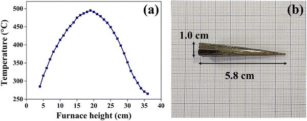 |
| | Fig. 1 (a) Axial temperature profile of the growth furnace and (b) the grown CuSbSe2 ingot crystal. | |
The bottom part of the ampoule was positioned within the upper zone at a maximum temperature of 15 °C above the melting point of the CuSbSe2 material. The molten material in the ampoule was allowed to settle for a period of 24 hours in the high temperature zone to maintain thermal equilibrium. Employing a stepper motor, the ampoule was cautiously descended from the higher temperature zone to the lower temperature zone at a controlled rate of 1 mm h−1. The lowering process is sustained for seven consecutive days at a consistent rate of lowering. Towards the end of the crystal growth process, the molten material underwent crystallisation. The furnace temperature was then gradually reduced to reach ambient temperature at a controlled rate of 10 °C hour−1 to prevent any formation of cracks in the crystal structure. Fig. 1(b) shows the CuSbSe2 ingot crystal grown by the vertical Bridgman technique within a quartz ampoule with a diameter of 1.0 cm and length of 5.8 cm. The smooth and lustrous surfaces obtained upon cleaving this crystal are employed for all characterisation techniques used in this work.
3. Characterisation
The powder X-ray diffraction (XRD) pattern of the grown CuSbSe2 crystal was recorded using a D8-Advance X-ray diffractometer using monochromatic CuKα radiation (λ = 1.5406 Å) at 40 mA and 40 kV, spanning a 2θ range from 10° to 90°. Subsequent analysis of the recorded XRD pattern was then performed utilising the powder-X software. The elemental composition and surface morphology of the grown single crystal were examined using an energy dispersive X-ray spectrometer (EDAX) combined with a field emission scanning electron microscope (FESEM) Nova nano FEG-SEM 450. The intricate structural attributes of the grown crystal are examined through high-resolution transmission electron microscopy (HRTEM) and selected area electron diffraction (SAED) employing a Thermo Scientific Talos F200i S/TEM instrument. The Raman spectrum was recorded using the HORIBA Xplora plus with a 532 nm excitation source. The reflectance spectrum of the CuSbSe2 crystal was acquired over a wavelength range of 200 nm to 1200 nm using a PerkinElmer Lambda-19 UV-vis-NIR spectrophotometer. The thermal stability of the CuSbSe2 crystal was analysed utilising the Seiko SII-EXSTAR TG/DTA-7200 thermal analyser. The thermal curves were recorded in a nitrogen (N2) gas environment at four different heating rates of 5, 10, 15 and 20 K min−1 across a temperature range from ambient to 723 K. Measurements of the temperature dependent electrical conductivity (σ), Seebeck coefficient (S) and thermal conductivity (κ) were conducted using setups designed by Supernova Technology, Vithal Udyognagar, Gujarat, India. These measurements were taken across a temperature range extending from ambient conditions to 585 K, oriented perpendicular to the c axis of the crystal planes. In photodetector fabrication, the CuSbSe2 crystal surface obtained from cleaving the ingot is used. For easier connection to the Keithley 4200-SCS, the crystal mounted on a mica sheet was attached on a printed circuit board. The crystal was then subjected to white light irradiation at varying bias voltages for the purpose of studying its photoresponse behaviour.
4. Results and discussion
4.1. Structural characterisation
4.1.1. X-ray diffraction (XRD).
The XRD pattern of the CuSbSe2 crystal in its powder form is presented in Fig. 2 along with the bottom portion displaying its standard reference pattern (JCPDS: 75-0992). The diffraction peaks in Fig. 2 correspond precisely to the orthorhombic crystal structure of CuSbSe2,27 indicating that the as-grown crystal was phase-pure CuSbSe2, devoid of any impurities or secondary phases such as Cu2Se,28 Sb2Se3,29 Cu3SbSe430 and Cu3SbSe3.31 The XRD pattern exhibited sharp and prominent peaks, indicating its highly crystalline nature with the (112) plane showing the dominant peak. The calculated lattice parameters from the experimental diffraction pattern were found to be a = 4.034 Å, b = 6.457 Å, and c = 14.929 Å, in good agreement with the JCPDS database and having the Pnma space group. The utilization of Debye Scherrer's formula32 yielded an estimated crystallite size of 22 nm for the (112) plane. The calculated values of lattice strain (ε), the dislocation density (δ)33 and unit cell volume34 for the CuSbSe2 single crystal are found to be 0.0082, 2 × 10¹⁶ m−2 and 388.86 Å3 respectively.
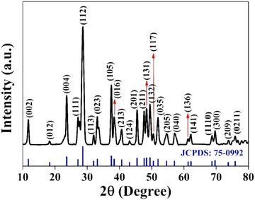 |
| | Fig. 2 The powder XRD pattern of the as-grown CuSbSe2 crystal. | |
4.1.2. Energy dispersive X-ray analysis (EDAX).
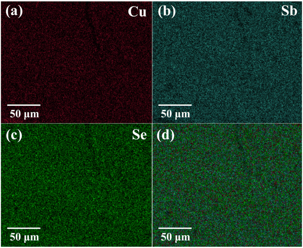
The obtained EDAX spectrum, as shown in Fig. 3, verifies the dominant presence of all three elements Cu, Sb and Se without any impurities, thereby indicating the purity of the sample. In the EDAX spectrum, Cu generates a strong signal at approximately 1 keV and another signal at around 8 keV, while Sb exhibits signals at about 4 keV and 1 keV, and Se shows signals at approximately 2 keV and 11 keV. The findings from the EDAX analysis of the CuSbSe2 single crystal corroborated the results of XRD and Raman spectroscopy, which will be discussed further. Additionally, the examination of the elemental and chemical composition of the grown crystal is also supported by elemental mapping. Fig. 4(a)–(d) show elemental mapping images of the CuSbSe2 single crystal, revealing the presence of its constituent elements Cu, Sb and Se through coloured representations. These images effectively demonstrate the even dispersion of these elements throughout. The computed weight percentage and atomic percentage of the CuSbSe2 single crystal are listed in Table 1. It is evident that the as-grown single crystal closely approaches stoichiometry in comparison to the ideal stoichiometric ratio of 1![[thin space (1/6-em)]](https://www.rsc.org/images/entities/char_2009.gif) :1:2 for CuSbSe2.35
:1:2 for CuSbSe2.35
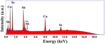 |
| | Fig. 3 The EDAX spectrum of the as-grown CuSbSe2 single crystal. | |
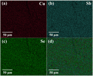 |
| | Fig. 4 The uniform distribution of (a) Cu (copper), (b) Sb (antimony), and (c) Se (selenium) and (d) overall distribution of Cu, Sb and Se elements throughout the area in the as-grown CuSbSe2 single crystal. | |
Table 1 Elemental analysis findings for the CuSbSe2 single crystal
| Element |
Observed wt% |
Standard wt% |
Observed at% |
Standard at% |
| Cu |
19.39 |
18.51 |
26.50 |
25.00 |
| Sb |
34.72 |
35.47 |
24.23 |
25.00 |
| Se |
45.89 |
46.01 |
49.27 |
50.00 |
4.1.3. Field emission scanning electron microscopy (FESEM).
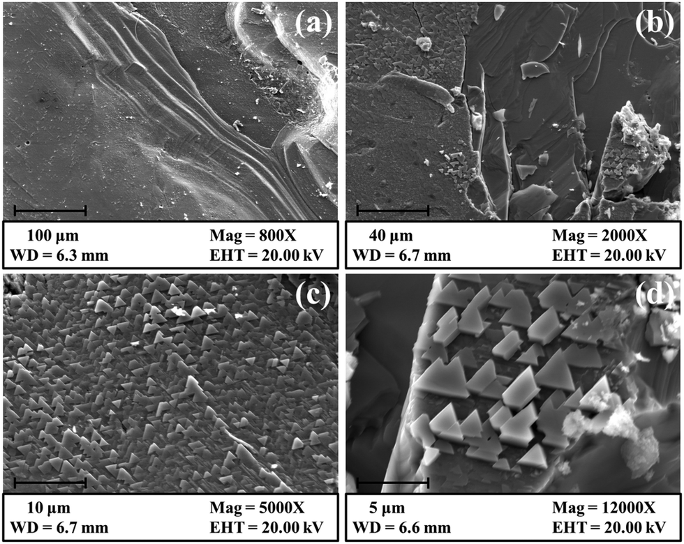
Photographs in Fig. 5(a)–(d) offer insights into the surface morphology of the grown CuSbSe2 single crystal at varying levels of magnifications. Fig. 5(a) and (b) shows that the surfaces are nearly flat and displays the presence of irregular termination of layers. Fig. 5(c) reveals the existence of numerous small triangular hillocks scattered across the flat surfaces of the grown single crystal. Fig. 5(d) provides an enhanced view of these triangular hillock structures present on the surface of the crystal. Collectively, these distinct features comprising flat surfaces, triangular hillocks and irregular layers ending on the flat surfaces suggest that the growth of the CuSbSe2 single crystal occurred through the sideway spreading of layers.36 The triangular hillocks on the flat surfaces emerge as a consequence of the rapid crystal growth, validating earlier findings regarding the uneven termination of layers.37 These flat surfaces ensure that the grown single crystal is well suited for photodetector device fabrication.
 |
| | Fig. 5 FESEM photographs of the as-grown CuSbSe2 single crystal taken at different magnifications. | |
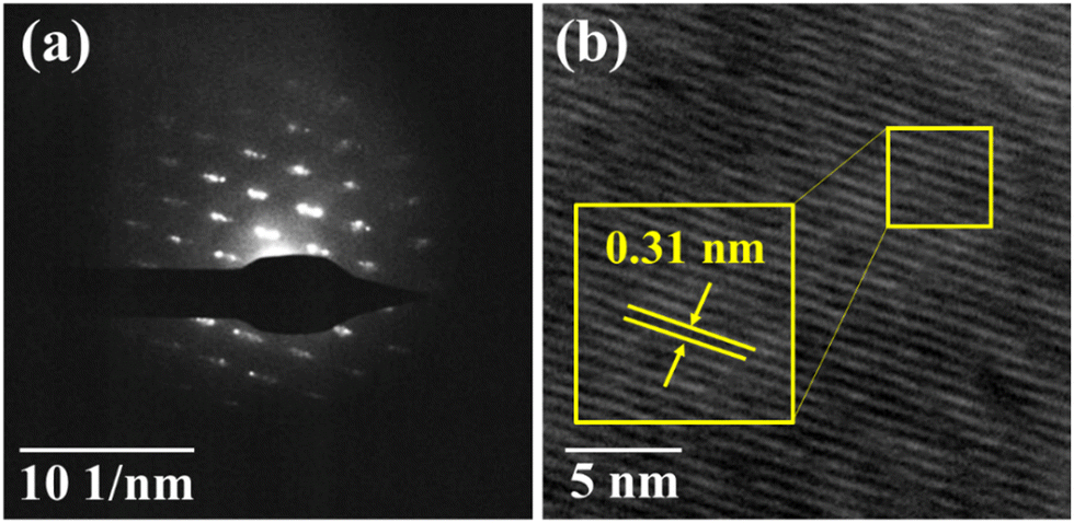
4.1.4. High resolution transmission electron microscopy (HRTEM) and selected area electron diffraction (SAED).
Fig. 6(a) illustrates the SAED pattern, revealing the crystalline nature of the grown crystal sample through distinct and well defined diffraction spots. This pattern aligns with the results from X-ray diffraction (XRD), providing further evidence for the presence of an orthorhombic lattice structure. In Fig. 6(b), the lattice fringe pattern is depicted, showing symmetrically arranged fringes that validate the crystalline nature of the sample. The observed fringe pattern in the HRTEM corresponds to a d-spacing value of 0.31 nm, consistent with the d-spacing value obtained for the prominent (112) plane in XRD analysis.
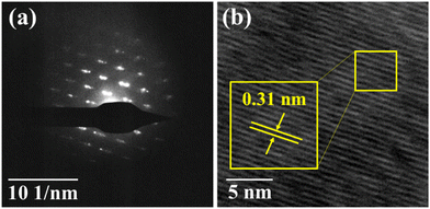 |
| | Fig. 6 (a) SAED pattern and (b) fringe pattern of the as-grown CuSbSe2 single crystal. | |
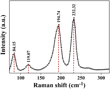
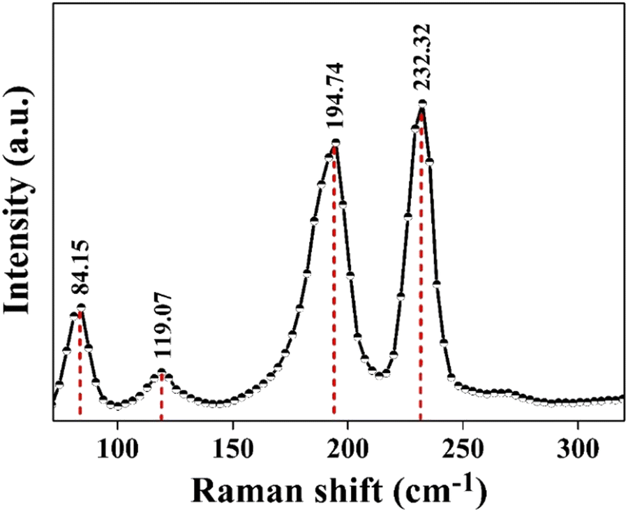
4.1.5. Raman spectroscopy.
The Raman spectrum, depicted in Fig. 7, is recorded at room temperature to elucidate the vibrational modes present in the grown crystal. The primitive cell of CuSbSe2 contains 16 atoms, resulting in a total of 48 modes within the phonon spectrum. Among these, three are acoustic modes, which exhibit values of zero at the Γ point. The irreducible representation of the phonon modes at the Γ point in the chalcostibite structure can be expressed as follows:19| | | Γ = 8Ag + 4Au + 4B1g + 7B1u + 8B2g + 3B2u + 4B3g + 7B3u | (1) |
for optical phonons andfor acoustic phonons. The vibrational modes B1u, B2u, and B3u are infrared (IR) active (excluding acoustic modes), while modes Ag, B1g, B2g, and B3g are Raman active; additionally the mode Au is classified as neither IR nor Raman active, making it a silent mode. The Raman spectrum of the CuSbSe2 single crystal displays peaks at 84.15 cm−1, 119.07 cm−1, 194.74 cm−1 and 232.32 cm−1, matching well with previously reported values for the orthorhombic phase of CuSbSe2.19 Notably, two highly intense peaks at 194.74 cm−1 and 232.32 cm−1 are attributed to Ag symmetry, representing Raman active modes.38 Additionally, two less intense peaks at 84.15 cm−1 and 119.07 cm−1 are also identified as characteristic peaks of the orthorhombic phase of CuSbSe2.39 The distinct sharp peaks in the spectrum indicate the high crystallinity of the grown single crystal. Furthermore, the absence of other peaks corresponding to different phases such as Sb2Se3 (188 cm−1 and 251 cm−1)40 and Cu3SbSe3 (250 cm−1, 372 cm−1 and 450 cm−1)41 indicates the single phase of CuSbSe2. Consequently, the combined evidence from Raman analysis and XRD solidifies the confirmation of pure orthorhombic chalcostibite CuSbSe2 phase formation.
 |
| | Fig. 7 The Raman spectrum of the grown CuSbSe2 single crystal. | |
4.2. Optical properties
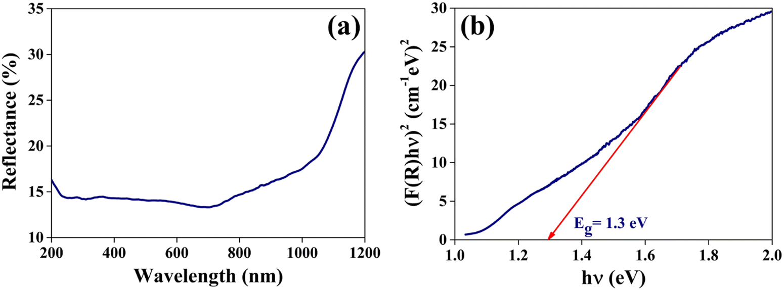
4.2.1. UV-vis-NIR spectroscopy.
In order to delve into the optical properties of the grown CuSbSe2 crystal, a reflectance spectrum is recorded in the range of 200 nm to 1200 nm. The spectrum illustrated in Fig. 8(a) indicates a gradual rise in reflectance starting from 200 nm and progressively increasing as it approaches higher wavelengths. The sharp edge reflectance combined with a linear tail feature serves as an indicator of the well defined crystalline nature of the grown CuSbSe2 single crystal, thereby providing support to the findings of our XRD and Raman analyses. The determination of the band gap of CuSbSe2 is carried out using the Kubelka–Munk equation based on the reflectance spectrum.42| | | (F(R)hν) = A(hν − Eg)n | (3) |
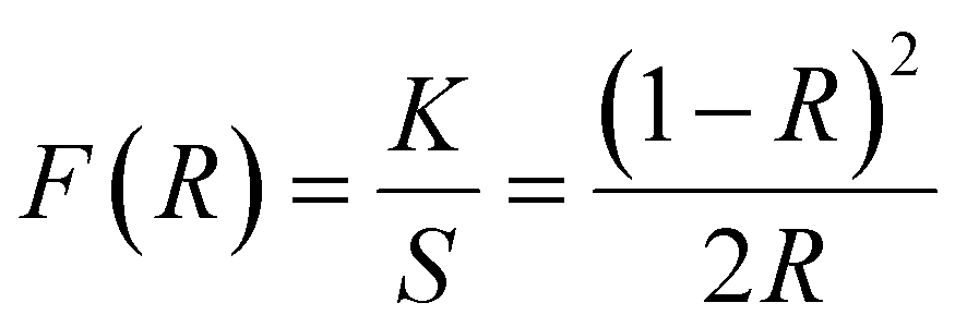
In this equation, the Kubelka–Munk function is denoted as F(R), ν represents the frequency of the photon, and hν corresponds to the energy of the incident photon. The exponent ‘n’ is indicative of the nature of the electronic transition, with values of either 1/2 or 2, signifying whether the transition is indirect or direct, respectively. The Kubelka–Munk function F(R) is represented as follows,43| | 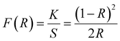 | (4) |
In the above equation, R signifies the diffuse reflectance, while K and S represent the absorption and scattering coefficients, respectively.
 |
| | Fig. 8 (a) The optical reflectance spectrum and (b) (F(R)hν)2versus hν plot of the grown CuSbSe2 single crystal. | |
In order to determine the bandgap, a plot of (F(R)hν)2 against hν is constructed as shown in Fig. 8(b). The extrapolation of the linear segment on the photon energy scale yields a bandgap (Eg) value of 1.3 eV and matches closely with previously reported values.38 This calculated bandgap reflects that the material can be used for solar cell and photodetector applications.
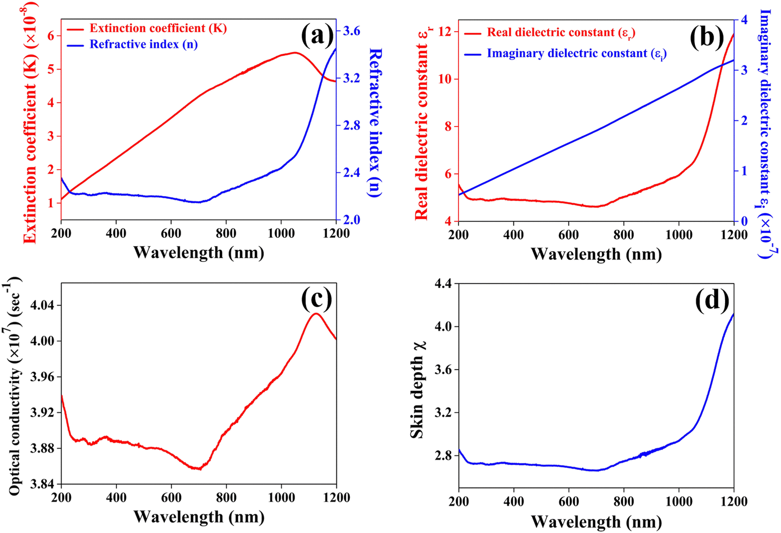
The extinction coefficient quantifies the decline in electromagnetic energy or light per unit thickness or distance within a particular medium, attributable to both absorption and scattering phenomena. This parameter plays a pivotal role in elucidating the interaction and attenuation of light across various materials. Fig. 9(a) presents the computed values for the extinction coefficient (k) and refractive index (n) of the CuSbSe2 single crystal, as determined from the reflectance spectrum through the relationship provided in ref. 44. The graph distinctly shows a rapid escalation in the extinction coefficient as the wavelength extends up to 1050 nm, followed by a subsequent decline up to 1200 nm. The minimal value of the extinction coefficient could be linked to the limited interactions between photons and electrons within the crystal.
 |
| | Fig. 9 Plots of (a) extinction coefficient and refractive index, (b) real and imaginary dielectric constants, (c) optical conductivity and (d) skin depth as a function of wavelength for the CuSbSe2 single crystal. | |
The refractive index quantifies a material's capacity to propagate light and it is determined by comparing the speed of light in a vacuum with its velocity within the examined medium. No significant change is observed in the refractive index in the visible region of the spectrum. The apparent observation is the continuous increase in the refractive index n beyond 725 nm up to 1200 nm.
The following equations are employed to compute the complex relative dielectric constant of semiconductors:45
where
εr and
εi represent the real and imaginary parts of the complex relative dielectric constant respectively, while
n denotes the refractive index, and
k stands for the extinction coefficient.
Fig. 9(b) illustrates the calculated variation of the real and imaginary dielectric constants with the wavelength. It is apparent from the aforementioned equation that the real part is predominantly influenced by the refractive index and the influence of the extinction coefficient is so minor that it can be neglected. Within the range of 200–1200 nm, the real dielectric constant (
εr) of CuSbSe
2 varies from 5.51 to 11.91, while the imaginary dielectric constant (
εi) increases from 0.52 × 10
−7 to 3.21 × 10
−7 marked respectively by the red and blue lines in
Fig. 8(b).
As anticipated, the values of the real component are notably higher than those of the imaginary counterpart and with increasing wavelength, both the real and imaginary portions of the dielectric constant exhibit an upward trend on the graph. The notable higher dielectric constant of CuSbSe2 implies a reduced exciton binding energy, possibly leading to immediate separation between photogenerated electrons and holes.46 Particularly for potential photovoltaic materials, possessing a high dielectric constant is a desirable characteristic, as it indicates a greater capacity for charge screening and a reduction in charge carrier recombination rates.47 Consequently, CuSbSe2 emerges as a promising contender for achieving enhanced photovoltaic performance due to its high dielectric constant.
Along with these optical parameters, the variation of optical conductivity and skin depth as a function of wavelength is also calculated through the equations provided in ref. 48. Fig. 9(c) illustrates the wavelength dependent changes in the optical conductivity of the material. Initially, the optical conductivity of the CuSbSe2 single crystal remains relatively steady up to 600 nm, and from there it progressively rises above 700 nm. Interestingly, there is a significant decrease in optical conductivity within the wavelength range of 580 nm to 700 nm, attributed to the crystal's low absorbance in this specific region. The maximum optical conductivity value of the CuSbSe2 crystal is identified at 1126 nm, reaching a value of 4.031 × 10⁷ s−1. The higher optical conductivity value may be ascribed to the direct transfer of charges from the valence band to the conduction band.
Skin depth, also known as penetration depth, plays a crucial role in understanding photon absorption and transmission within a material due to its inherent microstructure and physical properties.49Fig. 9(d) illustrates the variation of the skin depth of the material as a function of wavelength. A notable observation is the increase in the skin depth of the CuSbSe2 crystal as the wavelength extends.
4.3. Thermoelectric properties
4.3.1. Thermoelectric power.
A comprehensive analysis of fundamental thermoelectric properties, viz. Seebeck coefficient, electrical conductivity, and power factor, has been performed. Fig. 10(a) depicts the schematic representation of the measurement setup to measure the Seebeck coefficient of the CuSbSe2 single crystal. Fig. 10(b) illustrates the behaviour of the Seebeck coefficient (S) as a function of temperature of the as-grown CuSbSe2 single crystal. The differential method is used for this measurement by maintaining a temperature gradient of 5 K to avoid thermal stress. The observed positive value of the Seebeck coefficient (S) signifies the presence of p-type conductivity of the as-grown single crystal.17 The Seebeck coefficient demonstrates a rise across the entire temperature range, a result of an increased concentration of hole carriers. This increase in the number of holes being thermally activated to higher-energy states contributes to an elevated average entropy of holes, leading to the gradual rise in the S values with rising temperature. Within the temperature range of 310 K to 586 K, the Seebeck coefficient of the pure CuSbSe2 single crystal exhibits variation from 217.57 to 2471.21 μV K−1.20 The significant value of the Seebeck coefficient confirms the material's effectiveness in generating thermoelectric voltage, making it an ideal candidate for thermoelectric applications.
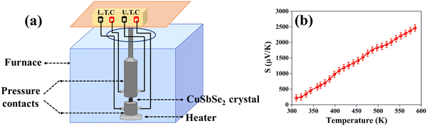 |
| | Fig. 10 (a) Schematic representation of the measurement setup to measure the Seebeck coefficient and (b) temperature dependent Seebeck coefficient of the as-grown CuSbSe2 single crystal. | |
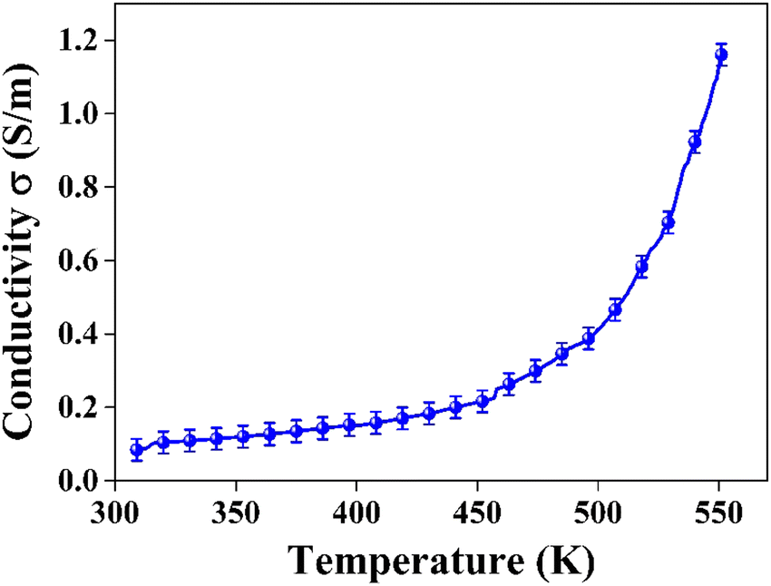
4.3.2 Electrical conductivity.
Fig. 11 presents the measured electrical conductivity of the CuSbSe2 single crystal within a temperature range from 310 K to 551 K. As depicted in the graph, an increasing trend is observed in the conductivity as temperature rises, indicative of the material's semiconductor nature. Notably, the sample exhibits a conductivity of 0.08 S m−1 at 310 K and is of the same magnitude as the reported conductivity of 0.04 S m−1 for near stoichiometric CuSbSe2 at room temperature.16 Furthermore, the conductivity value at 310 K for the CuSbSe2 single crystal is 0.08 S m−1, showing a subsequent increase to 1.16 S m−1 at 551 K.
 |
| | Fig. 11 Electrical conductivity ‘σ’ variation with temperature ‘T’ for the CuSbSe2 single crystal. | |
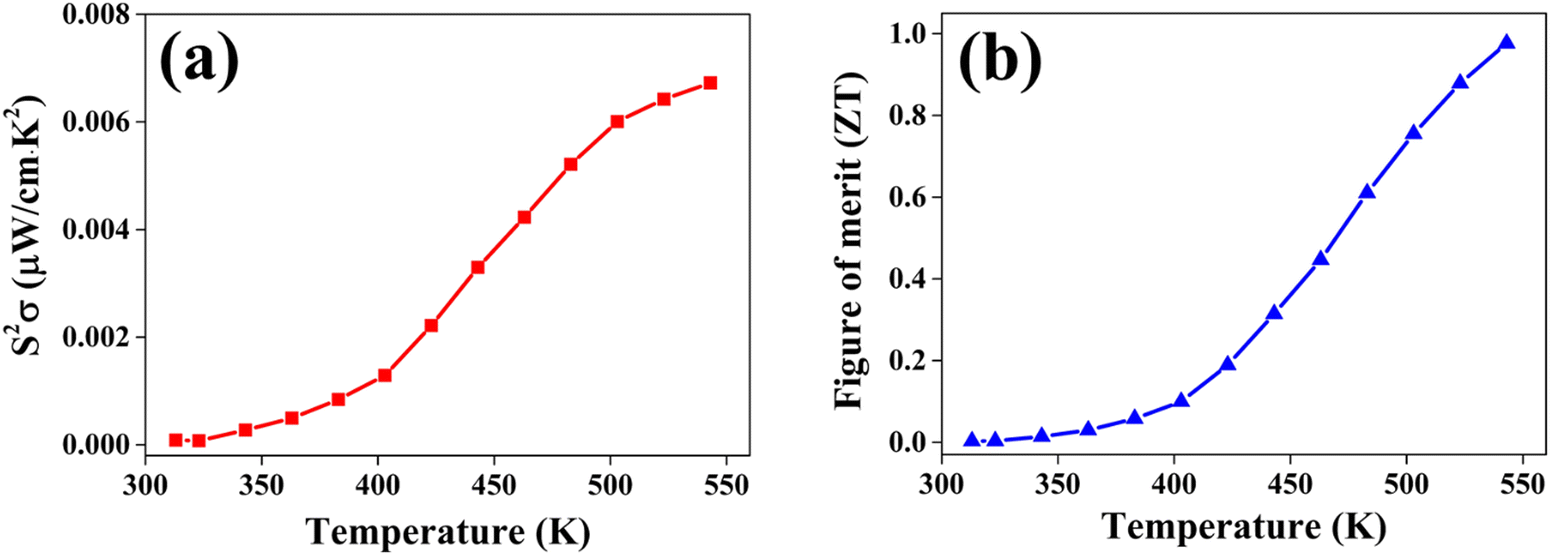
The power factor (PF) values were derived by combining the Seebeck coefficient and electrical conductivity, and a plot depicting their variation with temperature is provided in Fig. 12(a). At a temperature of 543 K, the observed value of power factor is 0.00672 μW cm−1 K−2.50 The rise in the power factor with temperature can be attributed to the increased electrical conductivity and Seebeck coefficient. The figure of merit (zT) is calculated using the below equation (eqn (7)).
| |  | (7) |
where ‘
S’ denotes the Seebeck coefficient, ‘
σ’ represents the electrical conductivity, ‘
κ’ is the thermal conductivity and ‘
T’ is the temperature.
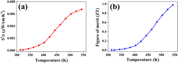 |
| | Fig. 12 (a) The power factor S2σ and (b) figure of merit zT variation with temperature T for the CuSbSe2 single crystal. | |
The calculated zT values were graphed in relation to temperature, as illustrated in Fig. 12(b). It is evident from the graph that the zT values display a rise corresponding to the increase in temperature. The sample demonstrated a peak value of zT of 0.976 at 543 K, which concurs with the reported values.20 For an ideal thermoelectric material, the figure of merit (zT) should ideally be ≥1 to achieve a conversion efficiency of >10%. The close proximity of the obtained zT value to 1 indicates that the grown CuSbSe2 single crystal exhibits promising characteristics as a thermoelectric material.
4.3.3. Thermal conductivity.
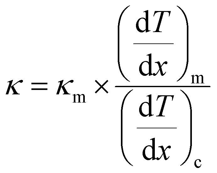
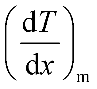
The computed total thermal conductivity of the CuSbSe2 single crystal is represented as a function of temperature in Fig. 13(a). As illustrated in the graph, thermal conductivity demonstrates an exponential decrease with rising temperature. This behavior is attributed to the Umklapp scattering, in which the phonon–phonon interactions become more dominant at a higher temperature.51 The value of κ for the CuSbSe2 single crystal is 8.54 W m−1 K−1 at 313 K, and this value decreases to 3.73 W m−1 K−1 at 543 K. The following formula was employed in the calculation of κ.52| | 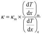 | (8) |
In the equation above, κm denotes the thermal conductivity of a brass rod (∼109 W m−1 K−1), while  and
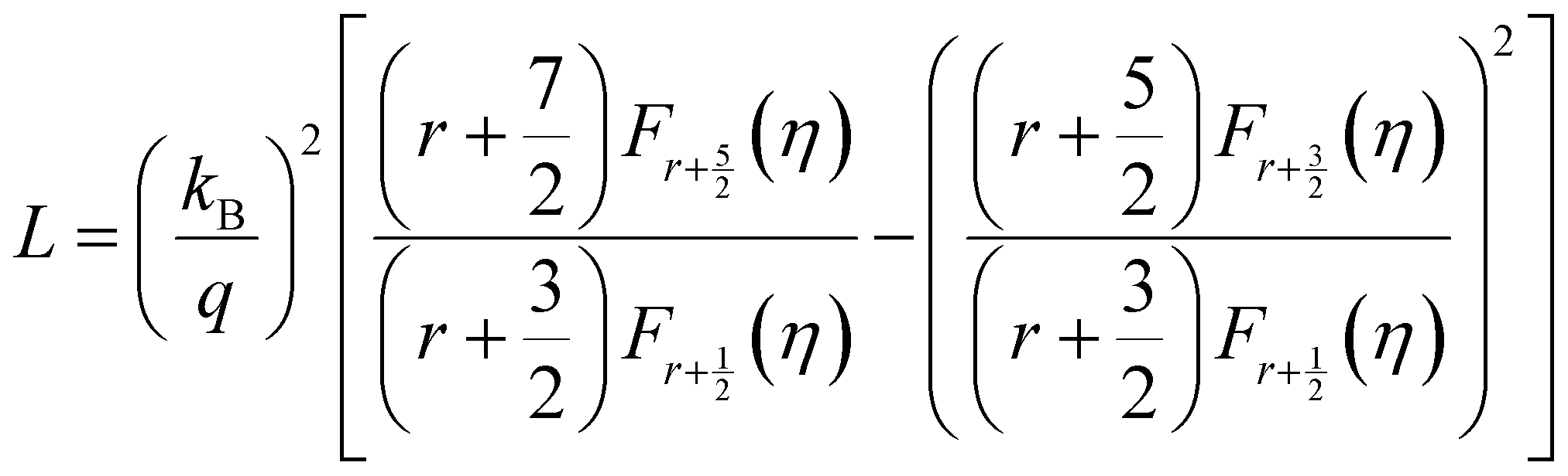
and  represent the temperature gradients across the brass rod and the crystal, respectively. The total thermal conductivity encompasses two components: the phononic contribution (κL) and the contribution of mobile charge carriers (κc), given as κtotal = κL + κc.53 Typically, κc can be estimated using the Wiedemann–Franz law, which links κc to the electrical conductivity via κc = LTσ.54 The Lorenz number, denoted as L, establishes a connection between a material's thermal conductivity and its electrical conductivity. The Lorenz number L can be determined through the single parabolic band (SPB) model, using the corresponding expressions as follows:55
| |  | (9) |
where η = μ/kBT represents the reduced Fermi energy, r denotes the scattering factor, kB is the Boltzmann constant, and q is the electron charge. For non-degenerate semiconductors, the calculation of the Fermi–Dirac integral Fn(η) is conducted as follows:| |  | (10) |
Here n represents the order number, while ξ = E/kBT (E is the energy of states). The lattice thermal conductivity κL can be calculated through the equation κL = κtotal − κc and is displayed in Fig. 13(b). The graphical representation reveals a diminishing trend of κL with increasing temperature, mirroring the behaviour of the total thermal conductivity. This decline at elevated temperatures can be attributed to the bipolar effect.51 Notably, the lattice thermal conductivity aligns closely with the values of the total thermal conductivity, indicating a minimal contribution from carriers. The relatively smaller values of κc are due to the low electrical conductivity.
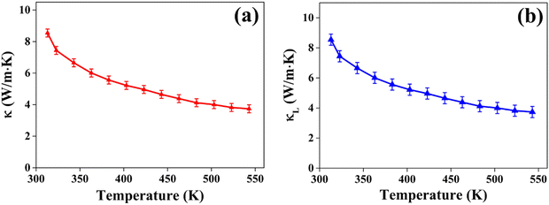 |
| | Fig. 13 The variation of (a) total thermal conductivity ‘κtotal’ and (b) lattice thermal conductivity ‘κL’ with temperature T for the CuSbSe2 single crystal. | |
4.4. Thermal analysis
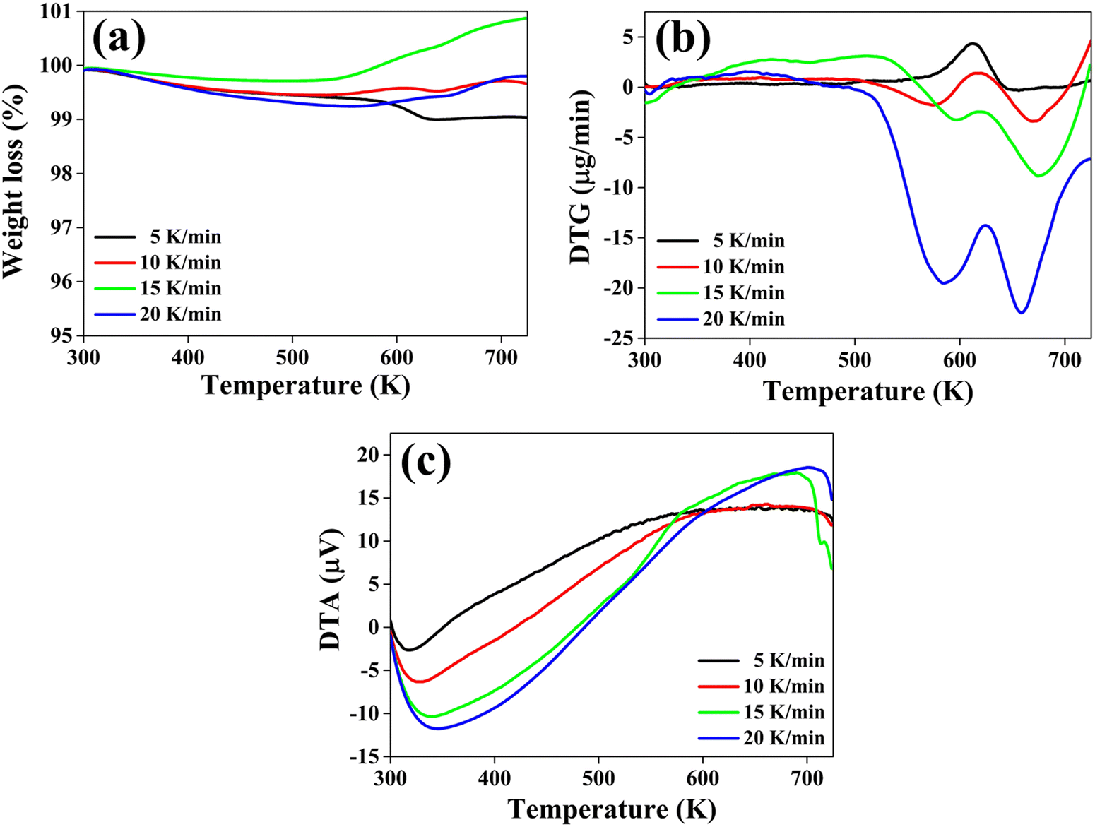
To determine the thermal stability of the material, the thermogravimetric (TG), differential thermogravimetric (DTG) and differential thermal analysis (DTA) curves of the CuSbSe2 crystal are recorded simultaneously under a N2 gas atmosphere. These thermo-curves are recorded across a temperature range from room temperature to 723 K, employing heating rates of 5, 10, 15 and 20 K min−1. The TG, DTG and DTA curves corresponding to these different heating rates are depicted in Fig. 14(a)–(c).
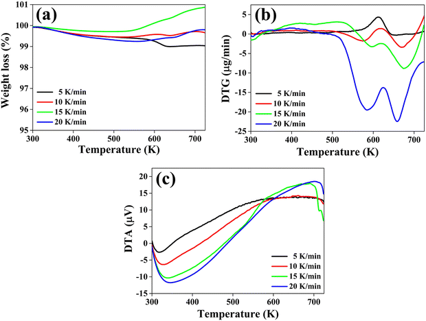 |
| | Fig. 14 (a) The TG, (b) DTG, and (c) DTA curves of the grown CuSbSe2 single crystal. | |
The thermogravimetric (TG) curve illustrates distinct behaviour in response to different heating rates for the sample. When heated at a slower heating rate of 5 K min−1, the sample experiences a continuous weight loss across the entire temperature range. Conversely, at the other three heating rates of 10, 15 and 20 K min−1 there is a weight gain along with weight loss. At 10, 15 and 20 K min−1 the material first loses weight until the temperature reaches 530 K, beyond which it undergoes weight gain until the temperature reaches 723 K. The corresponding percentage values of weight loss and gain are displayed in Table 2.
Table 2 Percentage (%) weight loss and gain in the corresponding temperature range for the CuSbSe2 crystal observed from TG curves
| Heating rate (K min−1) |
TG |
DTG peak positions Tm (K) |
| Weight loss (%) in the temperature range of 298–530 K |
Temperature range (531–723 K) |
| Weight loss (%) |
Weight gain (%) |
| 5 |
0.51 |
0.42 |
— |
612.39 |
| 10 |
0.48 |
— |
0.21 |
614.91 |
| 15 |
0.22 |
— |
1.15 |
617.32 |
| 20 |
0.64 |
— |
0.55 |
624.36 |
The initial marginal reduction in weight at all heating rates is attributed to the detachment of loosely bonded molecules from the crystal's surface.56 At the 5 K min−1 heating rate, weight loss at higher temperatures is attributed to sample decomposition. In the case of heating rates of 10, 15 and 20 K min−1, the weight gain can be attributed to the adsorption of nitrogen molecules.57 These molecules infiltrate the voids formed within the sample at the early stages of heating. Notably, the weight gain is more dominated for heating rates of 15 and 20 K min−1 compared to 10 K min−1, as shown in Fig. 14(a).
This distinction can be ascribed to the ease of interaction between the nitrogen gas molecules and the surface of the CuSbSe2 sample at higher heating rates. Such interaction is facilitated by the charge distribution within the N2 molecule. In contrast, the CuSbSe2 compound incorporates the chalcogen element (Se), which exhibits the characteristics of a soft Lewis base. This is indicated by the anion atom (Se2−) possessing lower electronegativity and higher polarizability, rendering it more susceptible to oxidation. Consequently, the internal structure of the compound becomes highly polarizable, resulting in an active nature of the sample surface. The favorable alignment of the quadrupole moment of N2 gas leads to its facile bonding with Lewis base natured CuSbSe2 through an orientation effect, particularly evident at higher temperatures.
As depicted in Fig. 14(b), the DTG plot indicated a prominent peak consistently appearing within the temperature range of approximately 612 K to 625 K at all heating rates. At both 5 K min−1 and 10 K min−1 heating rates, the DTG curve demonstrates an elevation above the zero baseline, aligning with the weight loss trend evident in the TG curve. Conversely, at heating rates of 15 K min−1 and 20 K min−1, the curve descends beneath the zero baseline, mirroring the weight gain observed in the TG curve within the same temperature span. The specific peak positions of the DTG curves at each heating rate are concisely compiled in Table 2.
As illustrated in Fig. 14(c), the DTA curve reveals distinctive thermal behavior exhibited by the CuSbSe2 single crystal sample. Initially, it displays endothermic characteristics, followed by a transition to an exothermic nature extending up to 723 K. The initial endothermic nature of the DTA curve signifies heat absorption by the sample. Within this temperature range, the heat absorption contributes to the expansion of voids formed due to the detachment of loosely bonded molecules. Consequently, these voids entrap N2 gas molecules, thereby corroborating the observed weight gain in the higher temperature range, as evidenced by the TG curves.
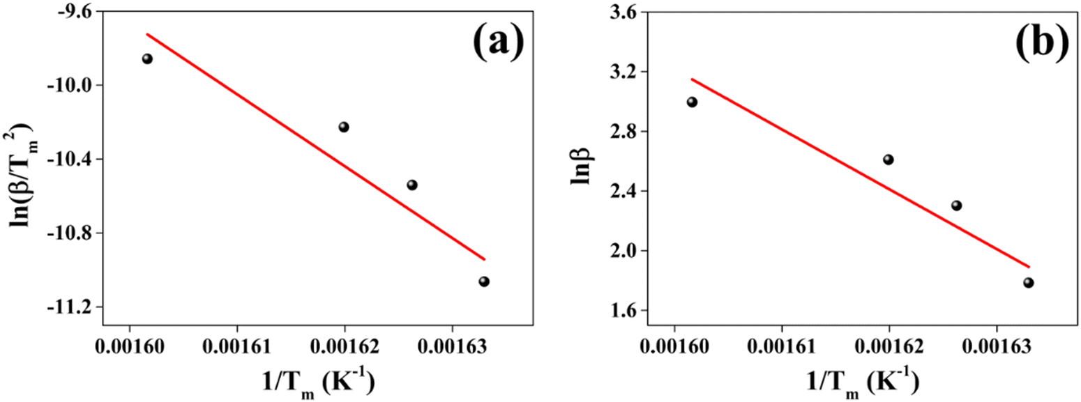
4.4.1. Kinetic parameters.
The investigation of kinetic parameters is done by the iso-conversional linear integral Kissinger technique and the Flynn–Wall–Ozawa (FWO) method.32,58 The outcomes obtained from these methodologies are presented in detail in Table 3 and displayed in Fig. 15(a) and (b) for the CuSbSe2 single crystal respectively. The slopes of these plots yield the activation energy (Ea), while the intercept of the plots provides the pre-exponential factor (A).59
Table 3 Kinetic parameters of the grown CuSbSe2 single crystal
| Method |
E
a (kJ mol−1) |
A (min−1) |
ΔH (kJ mol−1) |
ΔS (J mol−1) |
ΔG (kJ mol−1) |
| Kissinger |
323.29 |
2.58 × 1027 |
318.51 |
273.85 |
149.48 |
| FWO |
317.09 |
4.98 × 1024 |
311.95 |
221.82 |
175.03 |
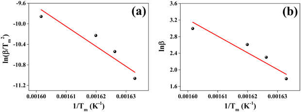 |
| | Fig. 15 (a) The Kissinger plot and (b) FWO plot of the grown CuSbSe2 single crystal. | |
The positive thermal activation energy Ea obtained for both methods signifies the initial temperature range of decomposition of the sample. This decomposition is supported by the weight loss evident in the TG curve. The positive enthalpy change ΔH indicates heat absorption by the sample. The absorption of heat is corroborated by the initial endothermic behavior of the DTA curve. The decomposition prompted by heat absorption leads to weight loss of the CuSbSe2 sample, as evidenced by the TG curves. The positive ΔS value suggests a state of increased disorder within the sample. This implies that rise in temperature reduces imperfection within the crystal structure. Additionally, the positive ΔG value indicates that the disintegration process is non-spontaneous. The thermal analysis indicates that the Bridgman grown CuSbSe2 single crystal remains suitable for device fabrication until the stability temperature of 530 K.
4.5. Electrical properties: I–V characteristics and pulse photoresponse
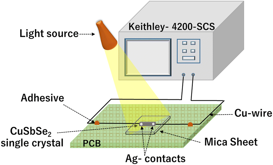
For the analysis of I–V characteristics, a CuSbSe2 single crystal is cleaved and affixed onto a mica sheet. Employing adhesive and highly conductive silver paste, two copper wires are affixed onto the crystal's upper surface, which has a surface area of 0.243 m2. The schematic depiction of the fabricated CuSbSe2 single crystal based photodetector in a parallel to planar configuration is presented in Fig. 16.
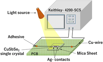 |
| | Fig. 16 Schematic representation of a CuSbSe2 crystal based photodetector and its connection with a Keithley-4200-SCS. | |
The parallel to planar configuration of a CuSbSe2 single crystal based photodetector is depicted in Fig. 17(a). The I–V curves of the CuSbSe2 single crystal are recorded under both dark and illuminated conditions with an intensity of 50 mW cm−2 using polychromatic light. Biasing voltages ranging up to ±500 mV are applied for this study, and the results are displayed in Fig. 17(b). The contact taken with silver paste on the CuSbSe2 single crystal shows ohmic contact behavior as evident from the I–V characteristics Fig. 17(b). The I–V curves highlight that under dark conditions, the measured current varies from −0.41 mA to +0.39 mA, whereas under illumination, the current increases from −1.01 mA to +1.03 mA for the parallel to planar configuration. This behavior is in accordance with the requirements for effective photodetection. The phenomenon is attributed to the generation of an increased number of photogenerated excitons under high voltage.60 Following their separation, these excitons diffuse towards the respective electrode sides under the influence of the applied external bias. These excitons play a crucial role in generating high photocurrents essential for optoelectronic devices. It is notable that as the applied biasing voltage surpasses 500 mV, saturation is observed in the CuSbSe2 single crystal photodetector. The discrepancy between the currents recorded under illuminated and dark conditions is used to compute the photocurrent (Iph).61
| | | Iph = Iilluminated − Idark | (11) |
The time-dependent photoresponse of the CuSbSe
2 single crystal is recorded under polychromatic light by employing a bias voltage of 100 mV for a time period of 20 s at an intensity of 50 mW cm
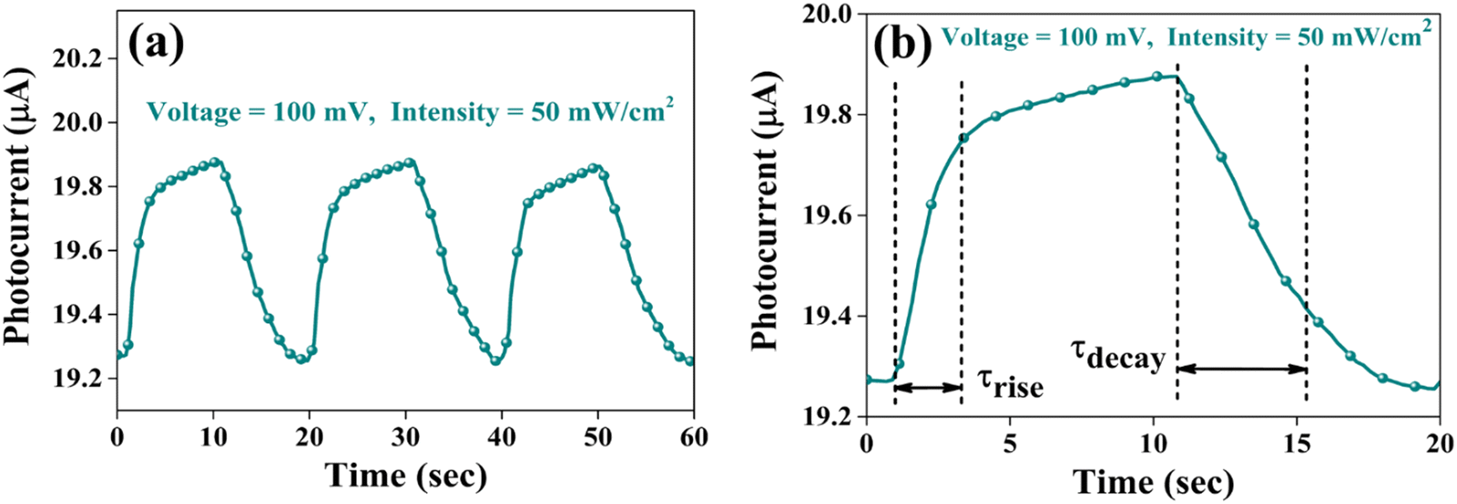
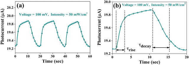
−2. The illumination is cyclically activated and deactivated at an interval of 10 seconds. To confirm the switching characteristics and consistency, the current rise (ON) and current fall (OFF) are recorded over numerous cycles and are shown in
Fig. 18(a). Each pulse represents the alternating on–off state, exhibiting the switching capability of the photodetector with consistent repeatability. The consistent performance of the photodetector and the increase in current with rising bias voltages indicate the favourable photoconducting behavior of a CuSbSe
2 single crystal-based photodetector. The semiconducting nature of the sample, along with efficient electron–hole pair separation, is attributed to the noticeable increase in current upon illumination.
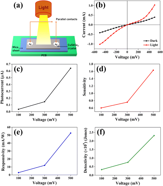 |
| | Fig. 17 (a) Schematic view of a CuSbSe2 single crystal based photodetector. (b) I–V characteristics of a photodetector under dark and illuminated conditions for the parallel to planar configuration and the variation of (c) photocurrent, (d) sensitivity, (e) responsivity and (f) detectivity as a function of voltage at a light intensity of 50 mW cm−2. | |
 |
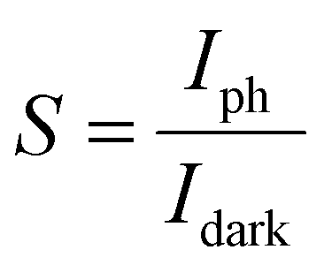
| | Fig. 18 (a) Pulse photoresponse at a 100 mV bias voltage and (b) magnified image of a single pulse for a 100 mV bias voltage of the CuSbSe2 photodetector. | |
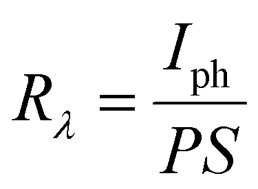
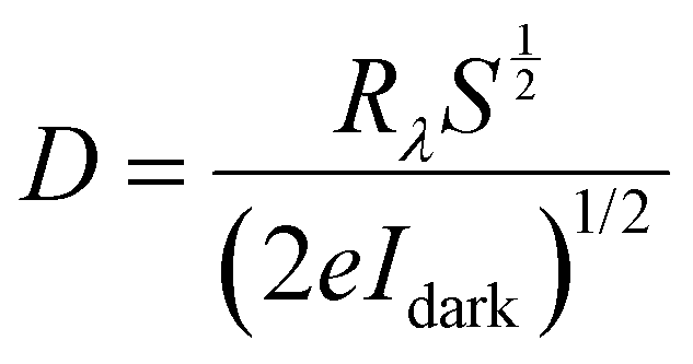
Sensitivity, responsivity (Rλ) and detectivity (D) stand as pivotal parameters for assessing the performance of the photodetector. Fig. 17(d)–(f) shows a graphical representation of sensitivity, responsivity and detectivity across various bias voltages. These parameters are determined using the below equations.62
| |  | (12) |
| |  | (13) |
| |  | (14) |
where ‘
P’ signifies the intensity of light, ‘
S’ designates the area of the device taken as 0.243 cm
2, ‘
Idark’ refers to the dark current and ‘
e’ represents the charge of an electron.
In Fig. 17(c), it can be observed that the increase in the bias voltage from 100 mV to 500 mV results in a progressive escalation of the photocurrent, ranging from 0.035 mA to 0.639 mA. This increased photocurrent can be ascribed to the diminished recombination of photogenerated excitons due to the high external bias.63 This effect facilitates a more effective separation of photogenerated excitons, consequently yielding a higher photocurrent. Furthermore, the increment in the photocurrent with different biases for the same illumination concurrently leads to increment in sensitivity and responsivity, as depicted in Fig. 17(d) and (e) respectively. The application of external bias also prompts a rise in dark current, thereby contributing to the improvement in detectivity, as illustrated in Fig. 17(f). Remarkably, the device achieved a maximum sensitivity of 1.631, a responsivity of 52.664 mA W−1 and a detectivity of 2.317 × 10⁹ Jones at a 500 mV bias voltage.
The response time is an another important parameter for detecting the incident radiation on the photodetector.64Fig. 18(b) presents the magnified image of a single pulse within the transient photoresponse recorded at a biasing voltage of 100 mV and an intensity of 50 mW cm−2. The photodetector exhibits a good rise time τrise (the amount of time required for 90% current to rise) of 2.248 s and a decay time τdecay (the amount of time required for 10% current to fall) of 4.273 s. At elevated temperatures, chalcogen vacancies contribute to a higher density of dislocations, leading to the formation of deep level defect states (DLDS) within the sample. These DLDS act as additional charge trapping centres, causing electrons generated upon illumination to become trapped before reaching the Ag electrodes. Consequently, the process of electron trapping and release by the defect states prolongs the response time of the detector, resulting in a slower overall response.65 A comparative analysis between certain photodetector parameters of previously reported bulk single crystal-based photodetectors and the corresponding parameters obtained from the present study is presented in Table 4. The CuSbSe2 material showed superior responsivity and detectivity in comparison to other photodetectors relying on bulk single crystals.
Table 4 Comparison of CuSbSe2 photodetector characteristics with previously published data
| Sample |
Source |
Bias voltage |
Intensity (mW cm−2) |
Responsivity (mA W−1) |
Detectivity (Jones) |
Ref. |
| CuSbSe2 crystal |
Visible light |
500 mV |
50 |
52.664 |
2.317 × 10⁹ |
Present work |
| CuSbS2 crystal |
Visible light |
10 mV |
50 |
0.558 |
32.84 × 10⁶ |
66
|
| MoSe2 crystals |
Visible light |
1 V |
90 |
7.38 × 10⁻³ |
2.98 × 10⁴ |
67
|
| SnS crystals |
670 nm wavelength |
Self-biased |
3 |
2.16 × 10⁻² |
5.06 × 10⁷ |
68
|
| Sb0.5Mo0.5Se2 |
Visible light |
1 V |
50 |
0.543 |
0.2 × 10⁷ |
64
|
| ZrS3 single crystals |
Visible light |
1 V |
120 |
0.120 |
6.43 × 10⁹ |
69
|
| SnS0.25Se0.75 crystals |
Visible light |
0 V |
60 |
67.11 × 10⁻³ |
— |
70
|
5. Conclusion
The vertical Bridgman technique led to the successful growth of a CuSbSe2 single crystal. The XRD analysis confirmed the crystal's orthorhombic structure, while EDAX provided insights into the crystal's stoichiometry and purity. The FESEM images of the single crystal showed smooth surfaces with layer formation. The single crystalline nature of the grown crystal is proved by the bright spot pattern of SAED. The SAED pattern additionally established that the crystal featured an orthorhombic lattice structure. Furthermore, the interplanar spacing obtained from the HRTEM analysis precisely complements the d-spacing data for the (112) plane. The Raman spectra displayed two predominant peaks at 194.74 cm−1 and 232.32 cm−1, which are associated with the Ag vibrational mode and orthorhombic phase of CuSbSe2. The reflectance spectra unveiled a direct optical bandgap of 1.3 eV. The semiconducting nature of the as-grown CuSbSe2 single crystal was verified through Seebeck coefficient measurement, confirming its p type characteristics. The CuSbSe2 single crystal exhibited S2σ and zT values of 0.00672 μW cm−1 K−2 and 0.976 at 543 K, respectively, which align with those of other reported materials. This underscores its potential as a suitable candidate for thermoelectric applications. Thermal gravimetric analysis (TG) of the CuSbSe2 sample, employing heating rates of 5, 10, 15 and 20 K min−1, confirmed its thermal stability up to 723 K. The photoresponse study using the CuSbSe2/Ag-paste/Cu wire under polychromatic light and dark conditions demonstrated its light sensing properties. At room temperature, employing a bias voltage of 500 mV with a light intensity of 50 mW cm−2 yields a responsivity and detectivity of 52.664 mA W−1 and 2.317 × 10⁹ Jones for the parallel to planar configuration. This further accentuates the material's possible utility as a photodetector. This research underscores the potential of the Bridgman grown CuSbSe2 single crystal as a promising contender within the realm of thermoelectric materials and photodetectors.
Author contributions
ZRP participated in the materials preparation, data collection, analysis, and writing of the original draft. MPD acquired resources and assisted in project administration, writing, reviewing, and editing of the manuscript, and supervision. SVB participated in the conceptualization, investigation, data analysis, and methodology. RMK participated in the materials preparation, data collection, and analysis. HRB participated in the data collection, methodology and manuscript reviewing. YVJ participated in the investigation and analysis. SHC participated in acquiring resources and reviewing the manuscript. SJP acquired resources and assisted in project administration.
Conflicts of interest
The authors declare that they have no known competing financial interests or personal relationships that could have appeared to influence the work reported in this paper.
Acknowledgements
One of the authors, ZRP, is thankful to the Education Department, Government of Gujarat, India for providing the Research Fellowship under SHODH (Scheme of Developing High Quality Research, Grant No. 2021016412) to carry out the research work. All the authors are thankful to the Sophisticated Instrumentation Centre for Applied Research & Testing (SICART), Vallabh Vidyanagar, Gujarat, India for EDAX, HRTEM, UV-vis and FESEM analyses, P. G. Department of Physics, Sardar Patel University, Vallabh Vidyanagar, Gujarat, India for XRD, Raman and TG analyses and P. G. Department of Applied & Interdisciplinary Sciences, CISST, Sardar Patel University, Vallabh Vidyanagar, Gujarat, India for the I–V characteristics study of our sample.
References
- M. Yue, H. Lambert, E. Pahon, R. Roche and S. Jemei, Hydrogen energy systems: a critical review of technologies, applications, trends and challenges, Renewable Sustainable Energy Rev., 2021, 146, 111180, DOI:10.1016/j.rser.2021.111180.
- S. R. Sinsel, R. L. Riemke and V. H. Hoffmann, Challenges and solution technologies for the integration of variable renewable energy sources d a review, Renew. Energy, 2020, 145, 2271–2285, DOI:10.1016/j.renene.2019.06.147.
- A. Tuan, V. V. Pham and X. Phuong, Integrating renewable sources into energy system for smart city as a sagacious strategy towards clean and sustainable process, J. Cleaner Prod., 2021, 305, 127161, DOI:10.1016/j.jclepro.2021.127161.
- K. Wang, M. Wu, Y. Sun, X. Shi, A. Sun and P. Zhang, Resource abundance, industrial structure, and regional carbon emissions efficiency in China, Resour. Policy, 2019, 60, 203–214, DOI:10.1016/j.resourpol.2019.01.001.
- P. K. Nayak, S. Mahesh, H. J. Snaith and D. Cahen, Photovoltaic solar cell technologies: analysing the state of the art, Nat. Rev. Mater., 2019, 4, 269–285, DOI:10.1038/s41578-019-0097-0.
- A. Manuscript, Multinary Copper-based Chalcogenide Nanocrystal Systems from the Perspective of Device Applications, Nanoscale Adv., 2020, 2(8), 3069–3082, 10.1039/D0NA00399A.
- L. Wang, Z. Guan and A. Tang, Multinary copper-based chalcogenide semiconductor nanocrystals: synthesis and applications in light-emitting diodes and bioimaging, J. Nanoparticle Res., 2020, 22, 28 CrossRef CAS.
- L. Zhang, X. Shi, Y. Yang and Z. Chen, Flexible thermoelectric materials and devices: From materials to applications, Mater. Today, 2021, 46, 62–108, DOI:10.1016/j.mattod.2021.02.016.
- M. Massetti,
et al., Unconventional Thermoelectric Materials for Energy Harvesting and Sensing Applications, Chem. Rev., 2021, 121(20), 12465–12547, DOI:10.1021/acs.chemrev.1c00218.
- T. Wang, C. Zhang, H. Snoussi and G. Zhang, Machine Learning Approaches for Thermoelectric Materials Research, Adv. Funct. Mater., 2019, 30(5), 1906041, DOI:10.1002/adfm.201906041.
- O. Caballero-calero, J. R. Ares and M. Martín-gonzález, Environmentally Friendly Thermoelectric Materials: High Performance from Inorganic Components with Low Toxicity and Abundance in the Earth, Adv. Sustainable Systems, 2021, 5, 2100095, DOI:10.1002/adsu.202100095.
- S. Perumal,
et al., Realization of High Thermoelectric Figure of Merit in GeTe by Complementary Co-doping of Bi and In Realization of High Thermoelectric Figure of Merit in GeTe by Complementary Co-doping of Bi and In, Joule, 2019, 3(10), 2565–2580, DOI:10.1016/j.joule.2019.08.017.
- C. Zhou,
et al., of merit greater than the single crystal, Nat. Mater., 2021, 20, 1378–1384, DOI:10.1038/s41563-021-01064-6.
- T. Xing,
et al., Ultralow Lattice Thermal Conductivity and Superhigh Thermoelectric Figure-of-Merit in (Mg, Bi) Co-Doped GeTe, Adv. Mater., 2021, 33(17), 2008773, DOI:10.1002/adma.202008773.
- B. Idris, A. Lawal, D. Abubakar and S. A. Dalhatu, Ab initio Calculation of CuSbSe2 in Bulk and Monolayer for Solar Cell and Infrared Optoelectronic Applications, Commun. Phys. Sci., 2021, 7(3), 229–240 CAS.
- S. Kim and N. Kim, CuSbSe2 Thin Films Prepared by Cosputtering Process for Absorber Layer in Solar Cells, Coatings, 2020,(62), 1–14 Search PubMed.
- N. Man,
et al., Thermoelectric Performance Optimization and Phase Transition of GeTe by Alloying with Orthorhombic CuSbSe2, ACS Appl. Energy Mater., 2021, 4, 4242–4247, DOI:10.1021/acsaem.1c00632.
- D. Goyal, C. P. Goyal, H. Ikeda, C. Gopalakrishnan and P. Malar, Materials Science in Semiconductor Processing Study of CuSbSe2 thin films grown by pulsed laser deposition from bulk source material, Mater. Sci. Semicond. Process., 2021, 121, 105420, DOI:10.1016/j.mssp.2020.105420.
- D. Xue, B. Yang, Z. Yuan, G. Wang, X. Liu and Y. Zhou, CuSbSe2 as a Potential Photovoltaic Absorber
Material: Studies from Theory to Experiment, Adv. Energy Mater., 2015, 5(23), 1501203, DOI:10.1002/aenm.201501203.
- T. Chen, H. Ming, B. Zhang, C. Zhu, J. Zhang, Q. Zhou, D. Li, H. Xin and X. Qin, Ultralow Thermal Conductivity and Enhanced Figure of Merit for CuSbSe2 via Cd-Doping, ACS Appl. Energy Mater., 2021, 4–10, DOI:10.1021/acsaem.0c02820.
- H. Yan, R. Xiao, Y. Pei, K. Yang and B. Li, Structural, electrical and optical characteristics of – CuSbSe2 films prepared by pulsed laser deposition and magnetron sputtering processes, J. Mater. Sci.: Mater. Electron., 2020, 31(1), 644–651, DOI:10.1007/s10854-019-02570-9.
- A. Romeo and E. Artegiani, CdTe-Based Thin Film Solar Cells: Past, Present and Future, Energies, 2021, 14(6), 1684 CrossRef CAS.
- N. Mufti, T. Amrillah and A. Taufiq, Review of CIGS-based solar cells manufacturing by structural engineering, Sol. Energy, 2020, 207, 1146–1157, DOI:10.1016/j.solener.2020.07.065.
- N. P. Raju and R. Thangavel, Theoretical investigation of spin e orbit coupling on structural, electronic and optical properties for CuAB2 (A¼ Sb, Bi; B ¼S, Se) compounds using Tran e Blaha-modi fied Becke e Johnson method: A first-principles approach, J. Alloys Compd., 2020, 830, 154621, DOI:10.1016/j.jallcom.2020.154621.
- A. Penezko, M. Kauk-Kuusik, O. Volobujeva, R. Traksmaa and M. Grossberg, Observation of photoluminescence edge emission in CuSbSe2 absorber material for photovoltaic applications Observation of photoluminescence edge emission in CuSbSe2 absorber material for photovoltaic applications, Appl. Phys. Lett., 2019, 115, 092101, DOI:10.1063/1.5114893.
- K. Abouabassi, A. Sala, L. Atourki and A. Soussi, Electrodeposited – CuSbSe2 thin films based solar cells on various substrates, J. Nanoparticle Res., 2022, 24(221) DOI:10.1007/s11051-022-05603-3.
- V. B. Ghanwat,
et al., Microwave assisted synthesis, characterization and thermoelectric properties of nanocrystalline copper antimony selenide thin films, RSC Adv., 2014, 4, 51632–51639, 10.1039/C4RA07609E.
- J. H. T. Daniel and V. B. K. Mohanraj, Enhanced Photosensitivity of Bi-Doped Cu2Se Thin Films Prepared by Chemical Synthesis for Solar Cell Application, Iran. J. Sci. Technol. Trans. A Sci., 2020, 44, 1369–1377, DOI:10.1007/s40995-020-00949-6.
- L. Xia, Z. Yang, B. Tang, F. Li, J. Wei and Z. Zhou, Carbon Nanofibers with Embedded Sb2Se3 Nanoparticles as Highly Reversible Anodes for Na-Ion Batteries, Small, 2021, 17(4), 2006016, DOI:10.1002/smll.202006016.
- W. Wang,
et al., Enhanced thermoelectric properties of Cu3SbSe4 via compositing with nano-SnTe, J. Alloys Compd., 2021, 878, 160358, DOI:10.1016/j.jallcom.2021.160358.
- A. A. Akl, I. M. El Radaf and A. S. Hassanien, An extensive comparative study for microstructural properties and crystal imperfections of Novel sprayed Cu3SbSe3 Nanoparticle-thin films of different thicknesses, Opt. - Int. J. Light Electron Opt., 2020, 165837, DOI:10.1016/j.ijleo.2020.165837.
- R. M. Kannaujiya, S. H. Chaki, A. J. Khimani, Z. R. Parekh and M. P. Deshpande, Kinetic stability of tin telluride nanoparticles synthesized by hydrothermal method, Chem. Thermodyn. Therm. Anal., 2022, 6, 100058, DOI:10.1016/j.ctta.2022.100058.
- K. Patel, G. Solanki, K. Patel, V. Pathak and P. Chauhan, Investigation of optical, electrical and optoelectronic properties of SnSe crystals, Eur. Phys. J. B, 2019, 92, 200 CrossRef CAS.
- Z. R. Parekh,
et al., CuO nanoparticles – Synthesis by wet precipitation technique and its characterization, Phys. B, 2021, 610, 412950, DOI:10.1016/j.physb.2021.412950.
- A. A. Hssi, N. Labchir, K. Bouabid, A. Almaggoussi and E. Gilioli, Anealing Effect on One step Electrodeposited CuSbSe2 Thin films, Coatings, 2022, 12(1), 75, DOI:10.3390/coatings12010075.
- M. P. D. Anilkumar, B. Hirpara, S. H. Chaki, A. J. Khimani and R. M. Kannaujiya, Thermal
Investigation of Direct Vapor Transport (DVT), Int. J. Thermophys., 2021, 42(2), 1–15, DOI:10.1007/s10765-020-02772-y.
- R. M. Kannaujiya, A. J. Khimani, S. H. Chaki, S. M. Chauhan, A. B. Hirpara and M. P. Deshpande, Growth and characterizations of tin telluride (SnTe) single crystals, Eur. Phys. J. Plus, 2020, 135(47) DOI:10.1140/epjp/s13360-019-00022-1.
- T. Guo,
et al., Materials Science in Semiconductor Processing Preparation and characterization of CuSbSe2 thin films deposited by pulsed laser deposition, Mater. Sci. Semicond. Process., 2021, 127, 105716, DOI:10.1016/j.mssp.2021.105716.
- C. C. Thinfilms, CHAPTER 4 GROWTH AND CHARACTERIZATION OF, 04, 4–6.
- P. Vidal-fuentes, M. Guc, X. Alcobe, T. Jawhari and M. Placidi, Multiwavelength excitation Raman scattering study of Sb2Se3 compound: fundamental vibrational properties and secondary phases detection Multiwavelength excitation Raman scattering study of Sb2Se3 compound: fundamental vibrational properties and Se, 2D Mater., 2019, 6(4), 045054, DOI:10.1088/2053-1583/ab4029.
- C. Wang,
et al., Dynamic disorder phonon scattering mediated by Cu atomic hopping and diffusion in Cu3SbSe3, npj Comput. Mater., 2020, 6, 155, DOI:10.1038/s41524-020-00421-4.
- B. Lakshmi, B. Joe and P. Gopinath, Accurate band gap determination of chemically synthesized cobalt ferrite nanoparticles using diffuse reflectance spectroscopy, Adv. Powder Technol., 2021, 32(10), 3706–3716, DOI:10.1016/j.apt.2021.08.028.
- S. Kumar, S. Tapash, C. Paul, S. Dutta and M. N. H. M. N. H. Mia, XRD peak profile and optical properties analysis of Ag-doped h-MoO3 nanorods synthesized via hydrothermal method, J. Mater. Sci.: Mater. Electron., 2020, 31(2), 1768–1786, DOI:10.1007/s10854-019-02694-y.
- V. Pathak, P. Lad, A. B. Thakkar, P. Thakor, M. P. Deshpande and S. Pandya, Synthesis, characterization and applications of cubic fluorite cerium oxide nanoparticles: a comprehensive study, Results Surfaces Interfaces, 2023, 100111, DOI:10.1016/j.rsurfi.2023.100111.
- W. Al-taa,
et al., Effect of Nano ZnO on the Optical Properties of Poly(vinyl chloride) Films, Int. J. Polym. Sci., 2014, 2014, 697809 Search PubMed.
- F. Yakuphanoglu, The determination of the optical constants of Cu(II) compound having The determination of the optical constants of Cu(II) compound having 1-chloro-2, 3-o-cyclohexylidinepropane thin film, Opt. Commun., 2004, 239, 275–280, DOI:10.1016/j.optcom.2004.05.038.
- N. S. Wadatkar and S. A. Waghuley, Complex optical studies on conducting polyindole as-synthesized through chemical route, Egyptian J. Basic Appl. Sci., 2015, 2(1), 19–24, DOI:10.1016/j.ejbas.2014.12.006.
- M. I. Fathima, A. M. S. Arulanantham and K. S. J. Wilson, Effect of ZnS nanowire ARC on CZTS/CdS thin fi lm solar cell by Nebulizer Spray Pyrolysis Technique, Mater. Res. Express, 2020, 7(1), 15510, DOI:10.1088/2053-1591/ab63f9.
- R. D. Prabu, S. V. I. Kulandaisamy and V. G. Mohd, Studies on copper oxide thin films prepared by simple nebulizer spray technique, J. Mater. Sci.: Mater. Electron., 2017, 28(9), 6754–6762, DOI:10.1007/s10854-017-6371-2.
- W. Fang, Y. Chen, K. Kuang and M. Li, Excellent Thermoelectric Performance of 2D CuMN2 (M = Sb, Bi; N = S, Se) at Room Temperature, Materials, 2022, 2, 1–13 Search PubMed.
- S. Patel, S. H. Chaki and P. C. Vinodkumar, Effect of sulphur doping in SnSe single crystals on thermoelectric power Effect of sulphur doping in SnSe single crystals on thermoelectric power, Mater. Res. Express, 2019, 6, 085910 CrossRef CAS.
- R. K. Giri, S. H. Chaki, A. J. Khimani and M. P. Deshpande, Mechanistic insights into transport properties of chemical vapour transport grown CuInS2 single crystal, J. Alloys Compd., 2023, 959, 170487, DOI:10.1016/j.jallcom.2023.170487.
- H. R. Bhoi,
et al., Investigation of thermoelectric properties and photoresponse of Sb2S32 × Sex crystals grown by Bridgman technique, J. Mater. Sci. Mater. Electron., 2023, 599, 126904, DOI:10.1007/s10854-023-10631-3.
- H. R. Bhoi,
et al., Effects of different Bismuth concentrations of InSbBi crystals grown by Bridgman technique, J. Cryst. Growth, 2022, 599, 126904, DOI:10.1016/j.jcrysgro.2022.126904.
- P. Chen,
et
al., Intrinsically Low Lattice Thermal Conductivity and Anisotropic Thermoelectric Performance in In-doped GeSb2Te4 Single Crystals, Adv. Funct. Mater., 2023, 33(11), 1–11, DOI:10.1002/adfm.202211281.
- R. M. Kannaujiya, S. H. Chaki and A. J. Khimani, Effect of Sb doping on CVT grown SnTe single crystals electrical and thermal properties, J. Mater. Sci. Mater. Electron., 2022, 33(26), 20823–20836, DOI:10.1007/s10854-022-08891-6.
- S. Patel, S. H. Chaki and P. C. Vinodkumar, Thermal analysis of direct vapour transport technique grown tin selenide single crystals, Thermochim. Acta, 2020, 689, 178614, DOI:10.1016/j.tca.2020.178614.
- G. H. Patel,
et al., Sol–gel synthesis and thermal characterization of SnO2 nanoparticles, Phys. B, 2021, 613, 412987, DOI:10.1016/j.physb.2021.412987.
- Z. S. Kachhia,
et al., Thermal decomposition study of cadmium telluride (CdTe), Mater. Today Proc., 2023 DOI:10.1016/j.matpr.2023.02.240.
- A. J. Khimani, S. H. Chaki, A. B. Hirpara, R. V. Patel and M. P. Deshpande, Enhancing photo-detection properties of Sb0.15Sn0.85S2 alloy, Mater. Res. Express, 2019, 6, 096303 CrossRef CAS.
- B. G. Valmik, M. P. Deshpande, S. V. Bhatt and V. Sathe, Investigation and fabrication of Cadmium Telluride (CdTe) single crystal as a photodetector, Phys. B, 2021, 614, 413027, DOI:https://doi.org/10.1016/j.physb.2021.413027.
- H. Patel, P. Chauhan, A. B. Patel and K. D. Patel, Regular Article – Solid State and Materials Anisotropic study of ReSe2-based photodetector grown via vapour transport technique, Eur. Phys. J. B, 2022, 95(11), 1–9, DOI:10.1140/epjb/s10051-022-00439-1.
- V. M. P. Kunjal Patel, P. Chauhan, A. B. Patel, G. K. Solanki and K. D. Patel, Orthorhombic SnSe Nanocrystals for Visible-Light Photodetectors, ACS Appl. Nano Mater., 2020, 3(11), 11143–11151, DOI:10.1021/acsanm.0c02301.
- V. Dixit,
et al., Growth and application of Sb0.5Mo0.5Se2 ternary alloy as photodetector, Mater. Lett. X, 2019, 2, 100013, DOI:10.1016/j.mlblux.2019.100013.
- K. Patel, G. K. Solanki, K. D. Patel and V. M. Pathak, X-ray diffraction analysis of hexagonal klockmannite cuse nanoparticles for photodetectors under UV light, J. Phys. Chem. C, 2021, 125(6), 3517–3526, DOI:10.1021/acs.jpcc.0c09353.
- Z. R. Parekh,
et al., Bridgman grown CuSbS2 single crystal and its application as photodetector and potential thermoelectric material, J. Alloys Compd., 2023, 171738, DOI:10.1016/j.jallcom.2023.171738.
- V. Dixit,
et al., Growth, characterization and photoconduction properties of Sb0.1Mo0.9Se2 single crystals grown by DVT technique, Mater. Sci. Semicond. Process., 2018, 88, 1–9, DOI:10.1016/j.mssp.2018.07.026.
- V. P. Jethwa,
et al., Applied Surface Science Temperature-dependent vibrational properties of DVT grown orthorhombic SnS single crystals and their application as a self-powered photodetector, Appl. Surf. Sci., 2020, 531, 147406, DOI:10.1016/j.apsusc.2020.147406.
- A. Patel,
et al., Low temperature anisotropic photoresponse study of bulk ZrS3 single crystal, Sens. Actuators, A, 2021, 331, 112969, DOI:10.1016/j.sna.2021.112969.
- V. P. Jethwa, K. Patel, V. M. Pathak and G. K. Solanki, Enhanced electrical and optoelectronic performance of SnS crystal by Se doping, J. Alloys Compd., 2021, 883, 160941, DOI:10.1016/j.jallcom.2021.160941.
|
| This journal is © The Royal Society of Chemistry 2024 |
Click here to see how this site uses Cookies. View our privacy policy here. 
 Open Access Article
 This Open Access Article is licensed under a Creative Commons Attribution-Non Commercial 3.0 Unported Licence
 *a,
M. P.
Deshpande
*a,
Sandip V.
Bhatt
b,
Rohitkumar M.
Kannaujiya
a,
Hiteshkumar R.
Bhoi
a,
Yash V.
Joshi
a,
S. H.
Chaki
a and
Swati J.
Pandya
a
*a,
M. P.
Deshpande
*a,
Sandip V.
Bhatt
b,
Rohitkumar M.
Kannaujiya
a,
Hiteshkumar R.
Bhoi
a,
Yash V.
Joshi
a,
S. H.
Chaki
a and
Swati J.
Pandya
a


 and
and 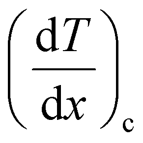 represent the temperature gradients across the brass rod and the crystal, respectively. The total thermal conductivity encompasses two components: the phononic contribution (κL) and the contribution of mobile charge carriers (κc), given as κtotal = κL + κc.53 Typically, κc can be estimated using the Wiedemann–Franz law, which links κc to the electrical conductivity via κc = LTσ.54 The Lorenz number, denoted as L, establishes a connection between a material's thermal conductivity and its electrical conductivity. The Lorenz number L can be determined through the single parabolic band (SPB) model, using the corresponding expressions as follows:55