DOI:
10.1039/D4MA00175C
(Paper)
Mater. Adv., 2024,
5, 5442-5457
Investigation of the structural, dielectric, magnetic properties and NTC-thermistor response of CaBiFeMnO6 double perovskites
Received
20th February 2024
, Accepted 3rd May 2024
First published on 7th May 2024
Abstract
To modify the physical properties through the cationic substitution of distinct elements at both the A and B sites, a novel polycrystalline double perovskite CaBiFeMnO6 was synthesized using an economical solid-state technique. According to Rietveld refinement analysis, the material crystallized in two orthorhombic phases. Field emission scanning electron microscopy images demonstrate that the mean crystalline size of the specimen is 754.265 nm and it has some porosity and a non-uniform distribution of grains on the surface. The unique transmittance, as observed in the Fourier transform infrared spectroscopy (FTIR) graph, suggests its perovskite background. The dielectric property analysis supported the exclusive negative temperature coefficient of resistance (NTCR) behaviour, confirmed by the impedance measurements in a defined temperature range for a specific electric field. The complex modulus analysis confirms the potential existence of a non-Debye-type relaxation mechanism. All of the characterizations, together with the high room temperature dielectric constant of 4023.194 with little tangent loss, suggested that the material could be a viable contender for use in different energy storage devices and supercapacitors. To illustrate the NTCR characteristic for NTC thermistor applications, the temperature coefficient of resistance (TCR) and thermistor constant (β) were calculated. The ferromagnetic nature of the prepared sample was verified through the M–H hysteresis loop.
1. Introduction
From circuit compensation to aerospace, temperature measurement, and control applications, the use of negative temperature coefficient (NTC) type thermistors is extensive and trusted as their reliability and accuracy make them an essential component in both industrial and domestic setups.1,2 Classifying the thermistors based on their temperature response, i.e., low and high NTC thermistors, expedites their applicability in different fields.3 Generally, low NTC thermistors rely on 3D transition-metal oxides such as Mn, Co, Fe, and Ni as these materials fall under the category of controlled valence semiconductors and exhibit a unique feature where their electrical resistance decreases exponentially as temperature increases up to 300 °C.3 The high NTC thermistors can usually respond to a higher temperature range (up to 1000 °C) and are composed of rare earth metals at the cationic sites of different oxide perovskites.4 Material scientists have been drawn to oxide perovskites because of their numerous intriguing physical characteristics, which include superconductivity, magnetoresistance, piezoelectricity, ferroelectricity, and half-metallic transport, among many others. Their relevance in various applications has made them a standout in the field of materials science. The preeminent motivation behind the diversified properties lies in the structural changes resulting from the substitutions at the cationic site in the preexisting perovskite materials. These modifications give rise to novel functional materials that possess exceptional properties, surpassing those of their predecessors.5 Investigating the versatile characteristics of uncomplicated perovskites either via co-substitution or doping is the earliest initiative towards a new era of perovskite materials. Researchers have discovered advanced characteristics that significantly improve the capabilities of these modified perovskites by transforming simpler materials into complex perovskites, including double perovskites. In the remarkable world of double perovskites, where the captivating empirical formula A2B2O6 unveils a new perspective on the traditional chemical formula of single perovskites (ABO3), both the A and B cationic sites can be seen as host positions, offering endless possibilities for exploration. By incorporating alkaline earth metals, alkali metals, and rare earth elements at the cationic sites, astounding advancements in behavioural changes have been achieved with double-ordered perovskites.5,6 Perovskites are capable of holding around 90% of metallic elements without undergoing structural damage; hence, modifying the chemical composition allows one to adjust their catalytic activity.3 A-site cationic substitutions play an important role in improving the electrical, magnetic, optical, and dielectric properties of perovskites, as in NaLaMgWO6,7 CaMnFeNbO6,8etc., whereas B-site substitution and doping, as in Bi2FeMnO6 and9 La2NiMnO6,10 has also attracted attention for their enhanced dielectric constant along with other incredible physical properties. Owing to their exceptional outcomes due to the inclusion of transition metal atoms with partially filled 3d orbitals at the B-site and Bi atoms with 6s2 lone pairs at the A-site, much attention has been given to the study of BiFeO3 (BFO) and BiMnO3 (BMO), which are considered groundbreaking magnetoelectric multiferroic materials that function at room temperature.11,12 Despite its lack of inherent ferromagnetism due to the Dzyaloshinskii–Moriya interaction, BiFeO3 does exhibit a moderate level of remanent magnetization ranging from 1 to 10 emu cm−3.13 Moreover, when it comes to BiMnO3, its ferromagnetic (FM) Curie temperature falls well below room temperature, at approximately 105 K. This limitation poses a technological challenge for the widespread use of BiFeO3 and BiMnO3 in advanced devices, but some earlier reported experimental details regarding Bi2FeMnO6 have disclosed its potential to be used as a new multiferroic material.14 The double perovskite structure Bi2FeMnO6 (BFMO) has been found to have an optical band gap energy of 1.23 eV and high dielectric permittivity (εr) values up to the order of 104, making it a promising material for a range of applications, including solar cells and sensors.11,12 A weak ferromagnetism is evident in the epitaxial BFMO thin film, with saturated hysteresis loops and small coercive fields at 200 K.14 With antiferromagnetic and ferromagnetic components, a coercive field of 118 Oe is reported as an unsaturated M–H hysteresis loop in BFMO double perovskite material.15 That's why the combined effect of the magnetic as well as dielectric nature of the material due to the inclusion of two different cations having different valences at both the larger and smaller cationic sites is the main highlight of this study. The addition of divalent Ca ion at the larger cationic site was intended to enhance the room temperature dielectric permittivity as well as the higher temperature permittivity. Although the magnetic nature of the given parent specimen is solely mediated by the B-site cationic attributes of Fe3+ and Mn4+, the stabilisation of single-phase Bi-based perovskites is quite challenging due to their inherent propensity for the formation of multiple phases and the volatile nature of bismuth. To overcome this hurdle, the strategic substitution of Bi3+ cations with alternative cations was the main motivation of our study. To enhance the stability and open up new possibilities for achieving reliable and durable perovskite structures, Ca2+ cation is partially substituted at the larger cationic site.
Although chemical routes ensure the purity of the prepared material, the solid-state reaction route is highly cost-effective and highly recommended for the synthesis of the solid solutions of different oxides using different metal salts, oxides, carbonates, nitrates, etc. The decomposition of these raw precursors also provides the desired solid material in a comparatively pure form. Moreover, the high crystallinity of the material is accommodated by this solid-state method of manufacturing. Considering these benefits of the conventional solid-state route, the desired double perovskite CaBiFeMnO6 is prepared using this synthesis technique.
The fundamental structural and microstructural elements along with the dielectric properties were explored extensively. The FTIR spectroscopic analysis, the impedance spectroscopy, and the conduction mechanisms of the prepared sample have been scrutinized. Additionally, a negative temperature coefficient thermistor application is discussed. In order to verify the effects of the substitutions at the two host positions, we focused primarily on the magnetic behaviour of the material. The enhanced magneto-dielectric effect of CaBiFeMnO6 is the major highlight of the present material along with the lower temperature range NTC thermistor application.
2. Experimental details
2.1. Synthesis of CaBiFeMnO6
Material fabrication methods, as well as excerption techniques, greatly influence physical properties. It requires a precise chemical equation to lead to the ideal perovskite material, in addition to a method for finding suitable raw precursors. Using calcium carbonate (CaCO3) (99.5%), bismuth oxide (Bi2O3) (99.5%), ferric oxide (Fe2O3) (98.5%), and manganese dioxide (MnO2) (99.5%) (M/S Loba Chemicals Co.) in the applicable amounts as raw materials, the desired product was prepared. The chemically balanced equation for the fabrication of the dual cationic substituted oxide perovskite CaBiFeMnO6 can be conveyed as follows.| | | 2CaCO3 + Fe2O3 + Bi2O3 + 2MnO2 → 2CaFeBiMnO6 + 2CO2↑ | (1) |
To ascertain the appropriate quantities of raw materials needed, detailed computations were performed. Using a chemical weighing scale, the precursor components were weighed according to their estimated stoichiometry, with an exactness of up to 3 decimal points. For almost two hours, the precursors were crushed and mixed using an agate mortar and pestle. The sample was then pestled for a further 2.5 hours, using the volatile reagent methanol. The ground powder then went through a heat treatment, i.e., calcination, step-by-step for 12 hours at 850 °C in a programmable furnace. The robust crystallinity of a solid solution is favoured by this solid-state technology-based fabrication method. Below this optimum temperature, i.e., 850 °C, the crystallinity of the desired solid solution would be compromised. The X-ray diffraction pattern revealed the phase evolution of the ground calcined composite which was obtained at room temperature in the wide diffraction angle (2θ) range of 20°–80° at a rate of scanning of 2° per minute.
After that, pelletization of the calcined product was performed to get cylindrical pellets of 13 mm × 1.5 mm using polyvinyl alcohol (PVA) as a volatile binding agent. These pellets were then sintered at 850 °C for a further 12 hours to densify the pelletized sample and to eradicate impurities in the prepared specimen. Fig. 1 is the schematic representation of the solid-state reaction method for the given specimen.
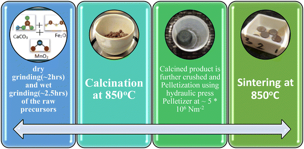 |
| | Fig. 1 Schematic diagram of the sample preparation method. | |
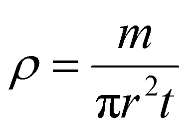
The density of the material was calculated from the sintered product using the standard expression of density, as follows.
| |  | (2) |
Considering the weight of the pellet (m), the surface area (πr2), and the thickness (t), the density is found to be 6.83 g cm−3 and the porosity of the material, calculated using the Archimedes method by submerging the material in water, is found to be 0.83 g ml−1.
2.2. Characterizations of the double perovskite material
The Rigaku Ultima-IV diffractometer, which is based on a radiation source of Cu-kα (λ = 1.5406 Å), was used to obtain the phase development and level of crystallisation in the fabricated specimen. For an extensive examination of the phase, an extended range of Bragg's angles, 20° to 80°, is utilised at a scanning rate of 2° per minute. To assay the electrical characteristics of the product, the dielectric behaviour and the loss tangent parameters were reported for a wide range of frequencies, where a polished and silver-pasted pellet was used as a specimen in the programmed LCR meter (HIOKI, Model: 1735, Japan). In addition to elemental analysis using electron dispersive spectroscopy (EDS), field emission scanning electron microscopy (FESEM) (Jeol FESEM Model JSM7610F Plus) was employed to explore the microstructural characteristics. The JASCO-FTIR/4100 infrared spectrometer was used to investigate the molecular vibrations of the material with excellent resolution. For the inquiry into magnetic characteristics, a Lake Shore 7410 vibrating sample magnetometer (VSM) was employed.
3. Results and discussions
3.1. Exploration of the crystal structure
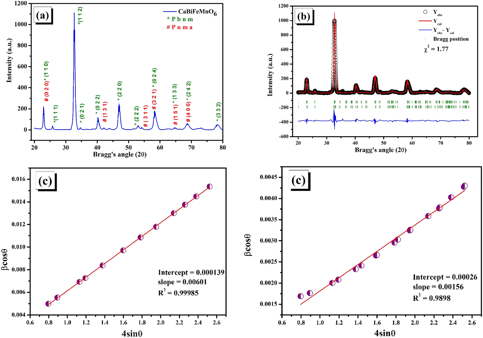
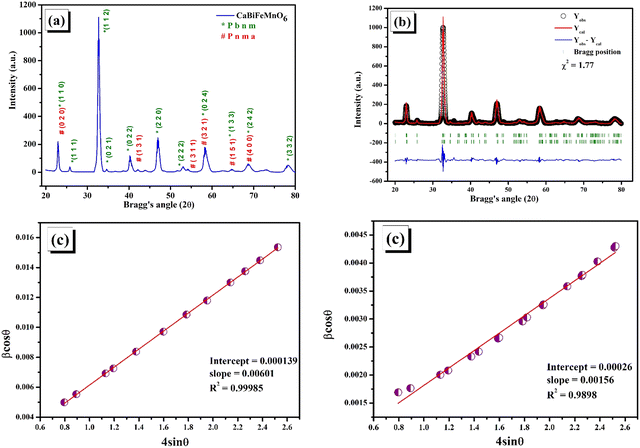
In order to truly understand the intricate nature of materials and how they form different phases, a thorough comprehension of the crystallographic data pertaining to the substance is necessary. This knowledge serves as a crucial foundation for comprehensive analysis. The elastic scattering of X-rays is a fascinating concept that proves incredibly useful in extracting valuable information about the intricate details of crystallographic structure. From crystal defects to unit cell parameters, strain, and chemical framework, this technique covers a wide range of aspects. The intensity pattern of X-ray diffraction for the calcined CaBiFeMnO6 (CBFMO) with varying Bragg's angle at room temperature is outlined in Fig. 2(a). The narrow, clear, and precise diffraction peaks unambiguously demonstrate the high crystallinity of the powdered sample, suggesting an ordered and well-structured arrangement of atoms inside the crystal lattice. The intensity pattern is inclined towards the development of an orthorhombic structure throughout an extensive range of Bragg's angle (20°–80°). The absence of any impurity peaks confirms the production of a highly pure version of CaBiFeMnO6. The Ca2+ ions included at the larger cationic site could be responsible for the formation of the orthorhombic phase of BiFeO3-based compounds instead of the basic rhombohedral phase. The geometrical framework of Goldschmidt's tolerance factor makes it possible to precisely evaluate the stability of perovskite crystalline formations. Reliable estimates of the structural integrity of the material can be assessed by considering their ionic radii. For doubly substituted perovskites, the tolerance factor may be stated mathematically in terms of the radii of the larger site substituted cations and smaller site substituted cations, rA, rA′, rB, and rB′, and the ionic radius of the oxygen ion is represented as ro.16| |  | (3) |
 |
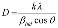
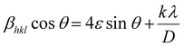
| | Fig. 2 (a) Indexed X-ray diffraction pattern of CaBiFeMnO6. (b) Rietveld refinement analysis of CaBiFeMnO6. (c) W–H plots for the Pbnm phase (left) and Pnma phase (right). | |
The ionic radii of the A-site cations Ca2+ and Bi3+ for the produced double perovskite material are 99 pm and 103 pm, respectively. O2− has an anionic radius of 135 pm, while the ionic radii of the B-site cations, Fe3+ and Mn4+, are 63 pm and 62 pm, respectively. The computed tolerance factor comes out to be 0.844, indicating the non-cubic structure of the material. For the specified oxide perovskite materials, all of these investigations revealed an orthorhombic crystal structure; hence, the X-ray diffraction data were refined under the presumption of the same crystal symmetry.
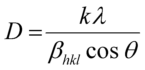
Using the Full Prof refinement programme, we carried out Rietveld refinement to obtain a thorough grasp of the phase structure and composition. Our findings are clearly illustrated by the data, shown in Fig. 2(b). As the crystallite size, defects, stress/strain, detector resolution, and (hkl) indexing are solely dependent on the peak shape of the analysis, it is the most significant parameter of Rietveld refinement. Introducing pseudo-Voigt as the peak function, which is the linear combinational product of both the Lorentzian and the Gaussian peak functions, Rietveld refinement was performed.17 Based on the data assessment, the refinement of the powder diffraction data crystal indicates a highly ordered and stable composition with the existence of two orthorhombic symmetric phases, i.e., the (Pbnm) and (Pnma) space groups. Initial refinement using only one phase referring to a Ca-based double perovskite, i.e., Pbnm, did not satisfy the existence of all the peaks, but the inclusion of the dual phase led to a proper and logical fitting of data with a lower value of χ2 which might be due to the convention of axes between the phases. The refined atomic positions of the constituent atoms for both the phases are given in Table 1, along with the corresponding Wyckoff positions obtained from the Bilbao Crystallographic Server. The accuracy of the analysis methods deployed can be verified by the reliability factors tabulated in Table 2. The refined cell parameters for both the orthorhombic crystal phases are reported in Table 2, where the lower values of error for each parameter point towards the precision of the refinement procedure. The lower value of χ2, i.e., 1.77, agrees with the fact that the as-prepared double perovskite material possesses two orthorhombic crystal phases. The indexing of the XRD peaks presented in Fig. 2(a) are the Miller indices corresponding to the Bragg's angle for the two phases, which we considered for the refinement of the powder diffraction data. Table 3 presented the atomic displacement parameters revealed by the refined experimental XRD data sets. Williamson–Hall (W–H) plot analysis was adopted to find the crystalline size and lattice strain associated with the reported crystal structure using the Debye–Scherrer equation in a modified form. The three types of models used in Williamson–Hall analysis are the uniform deformation model (UDM), uniform stress deformation model (USDM), and uniform deformation energy density model (UDEDM) to assess elastic characteristics including strain, stress, and energy density, respectively. In the size-strain plot, the size-broadened part is considered a Lorentzian function, and the strain-broadened part is considered a Gaussian function of the XRD peak profile. To estimate the average crystalline size (D) of the material, the Debye–Scherrer equation can be written as follows.18
| |  | (4) |
Table 1 Atomic positions and Wycoff positions of the given material refined in both Pbnm and Pnma phases
| Atoms |
Phase 1: Pbnm |
Phase 2: Pnma |
| Atomic positions |
Wyckoff positions |
Atomic positions |
Wyckoff positions |
|
x
|
y
|
z
|
x
|
y
|
z
|
| Ca |
−0.02562 |
0.04041 |
0.25 |
4c |
0.02033 |
0.25 |
0.99317 |
4c |
| Bi |
−0.02562 |
0.04041 |
0.25 |
4c |
0.02033 |
0.25 |
0.99317 |
4c |
| Fe |
0.5 |
0 |
0 |
4b |
0.5 |
0.5 |
0 |
4b |
| Mn |
0.5 |
0 |
0 |
4b |
0.5 |
0.5 |
0 |
4b |
| O1 |
0.09848 |
0.48624 |
0.25 |
4c |
0.46329 |
0.25 |
0.02115 |
4c |
| O2 |
0.69747 |
0.28406 |
0.02102 |
8d |
0.64337 |
0.38840 |
0.49537 |
8d |
Table 2 Refined cell parameters, angles, and reliability factors
|
|
Parameters |
Phase 1: Pbnm |
Phase 2: Pnma |
| Cell parameters |
a (Å) |
5.40339 ± 0.00287 |
5.49056 ± 0.00062 |
|
b (Å) |
5.51308 ± 0.00331 |
7.75325 ± 0.00076 |
|
c (Å) |
7.68927 ± 0.00196 |
5.41402 ± 0.00100 |
| Cell angles |
α
|
90 |
90 |
|
β
|
90 |
90 |
|
γ
|
90 |
90 |
| Reliability factors |
R
p
|
7.76 |
|
R
wp
|
11.14 |
|
R
exp
|
8.4 |
|
χ
2
|
1.77 |
Table 3 Refined atomic displacement parameters for each atom
| Atoms |
U
11 (Å2) |
U
22 (Å2) |
U
33 (Å2) |
U
12 (Å2) |
U
13 (Å2) |
U
23 (Å2) |
| Ca |
−0.015510 |
0.146930 |
0.017310 |
−0.007290 |
0.0000 |
0.0000 |
| Bi |
−0.015510 |
0.146930 |
0.017310 |
−0.007290 |
0.0000 |
0.0000 |
| Fe |
−0.31360 |
−0.001530 |
0.006310 |
0.029730 |
−0.008600 |
−0.009570 |
| Mn |
−0.31360 |
−0.001530 |
0.006310 |
0.029730 |
−0.008600 |
−0.009570 |
| O1 |
0.190180 |
−0.207730 |
0.299260 |
0.011790 |
0.0000 |
0.0000 |
| O2 |
0.0000 |
0.0000 |
0.0000 |
0.0000 |
0.0000 |
0.0000 |
The sole factor taken into account by the Debye–Scherrer formula is how crystallite size affects XRD peak broadening. It does not include details about the lattice microstructure, including intrinsic strain brought on by stacking faults, point defects, grain boundaries, or triple junctions. The Williamson–Hall method may be used to calculate intrinsic strain in addition to particle size by taking into account the impact of strain-induced XRD peak broadening. The uniform deformation model (UDM) takes into account uniform strain that develops in nanocrystals as a result of crystal defects across the crystallographic direction, i.e., it considers isotropic strain which influences XRD broadening.19 The combined effects of size and strain on the XRD peak broadening with a certain hkl value can be expressed as follows.
| | | βhkl = βsize + βstrain | (5) |
By incorporating the full-width half maxima (FWHM) (β) due to the lattice strain (ε) and the size effect, the W–H empirical relation can be described as follows.19–21
| |  | (6) |
Here, the shape factor
k is taken to be 0.89.
Fig. 2(c) showcases the two W–H plots for the as-prepared sample with dual phases, revealing valuable insights, with the best-fitted data having
R2 = 0.99985 for the
Pbnm phase and
R2 = 0.9898 for the
Pnma phase. By taking the X-ray wavelength (
λ) to be 0. 154 nm and analysing the
y-intercepts of the graphs plotted between 4
![[thin space (1/6-em)]](https://www.rsc.org/images/entities/char_2009.gif)
sin
θ and
βcos
θ, which were determined to be 0.000139 for the
Pbnm phase and 0.00026 for the
Pnma phase, we can calculate the crystalline sizes to be 981.23 nm and 527.3 nm, respectively. So, the average crystalline size of the synthesized sample is computed as 754.265 nm. The slopes of the graphs indicate the lattice strain values for the two phases,
i.e., 0.00601 and 0.00156, respectively, which suggest that the bonds are stretched. This strain could be attributed to the occupancy of two elements with distinct radii at the same cationic site.
Since a crystal is anisotropic, an anisotropic term should be included in the Williamson–Hall equation. This improved model, known as the uniform stress deformation model (USDM), has modest microstrain and considers the lattice deformation stress to be uniform along all lattice plane directions. Because of the size constriction, a small amount of internal stress develops with the intrinsic strain in the crystals. An anisotropic Young's modulus and the stress-induced broadening of the XRD peak were taken as factors for the USDM.19 The stress-modified W–H equation can be expressed in terms of the Young's modulus (Yhkl).
| |  | (7) |
The Young's modulus for an orthorhombic system can be calculated theoretically by considering the elastic compliances and the elastic stiffness constant.
3.2. Microstructural analysis using FESEM
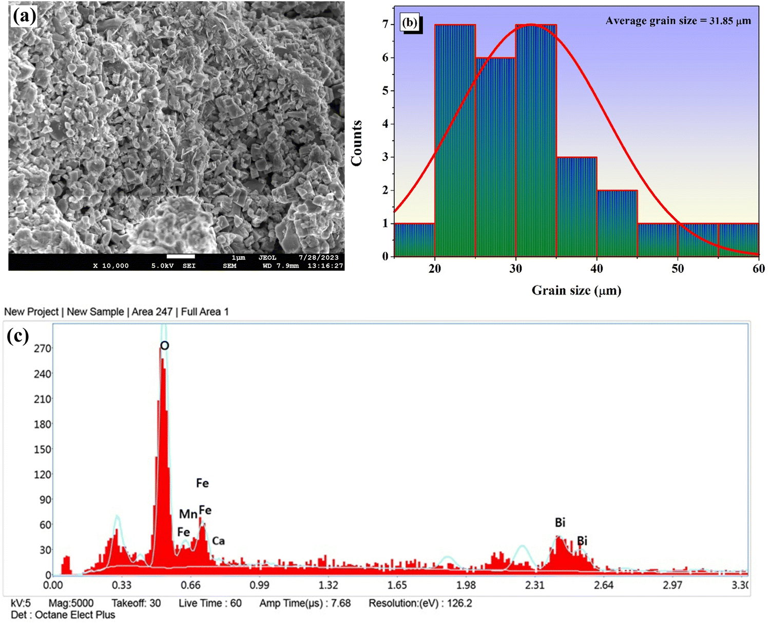
An inspection of the scanning electron micrograph reveals that the grains are distributed non-homogeneously and have distinct grain boundaries, as shown in Fig. 3(a). A surface coated with closely spaced distinct microparticles with different sizes and shapes with well-defined grain boundaries can be observed in the room-temperature FESEM micrograph. The grains have a modest porosity and are dispersed unevenly as an outcome of the inclusion of Fe3+. The appearance of the polycrystalline phase at different rates of growth is connected to the difference in grain sizes and shapes.22Fig. 3(b) depicts a representation of the histogram mapping of the grain sizes, obtained using the ImageJ program. The mean grain size is determined to be 31.85 μm by fitting the histogram data with a Gaussian function.
 |
| | Fig. 3 (a) FESEM image of CBFMO. (b) Histogram mapping for the grain size of the sample. (c) Surface elemental composition from energy dispersive X-ray spectroscopy analysis. | |
3.3. Elemental analysis by energy dispersive spectroscopy (EDS)
A qualitative method for verifying the existence of the intended elements of the prepared material is energy dispersive spectroscopy (EDS). The semi-quantitative results of EDS contribute to the analysis of the composition of the as-prepared product. The information on the constituents as recorded from a specific cross-sectional area of the SEM micrograph is shown in Fig. 3(c). The EDS data reveals that all of the components, i.e., Ca, Bi, Fe, Mn, and O, are present in the material, and the nonexistence of impurity peaks confirms the purity of the produced sample.
3.4. Fourier transform infrared spectroscopy analysis
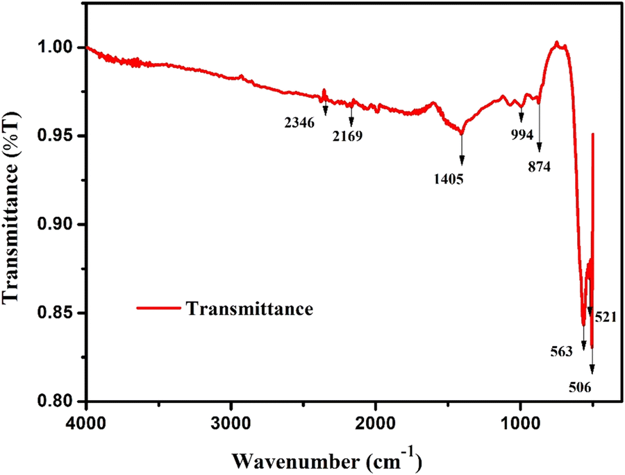
Thanks to the assistance of FTIR spectroscopic data, analysis of infrared absorption and emission spectra has become not only feasible but also remarkably insightful. By analysing the peaks at various wavenumbers, we gain valuable insights into the characteristics and behaviour of all the covalent bonds involved. This powerful tool allows for a comprehensive understanding of the material at a molecular level, aiding in various scientific investigations. In the present study, the FTIR information in terms of the transmittance (T) between 4000 cm−1 and 300 cm−1 is shown in Fig. 4. The vibrations within the range of 850–400 cm−1 are correlated with the specific type of lattice.23 In double-ordered perovskite materials, the existence of perovskite phases may be identified by detecting transmission bands at 874, 994, and 1405 cm−1.24 Since octahedral BO6 is associated with a larger concentration of charge carriers, the prominent peaks at 506, 521, and 563 cm−1 may be ascribed to the symmetrical stretching of BiO625,26 or the anti-symmetric oscillations of the MnO6 and FeO6 octahedrons.27 As the oscillation of phonons is associated with certain precise wavenumber ranges, it becomes simpler for researchers to accurately identify and analyse these materials. This illustrates the unique traits of the composition of the material and its vibrational properties.28 Fe–O octahedral bonds have been determined to be the origin of the stretching vibrations in the current sample at wave numbers 874 and 994 cm−1. Furthermore, the overtones of strong C–O bond vibrations related to carbonate ion (CO32−) vibration were identified as the cause of the peak at 1405 cm−1.28 These results point to a complicated molecular structure and emphasize how crucial these vibrational modes are to comprehending the chemical composition and behaviour of the sample. The data presented here suggests that the distinctive vibrations at 2169 and 2346 cm−1 are vibrations caused by defects in the prepared sample.28
 |
| | Fig. 4 FTIR pattern of the prepared sample. | |
4. Dielectric property study
Using a pre-defined equation regarding the dielectric characteristics of a material, the complex dielectric function in an applied field can be represented aswhere the imaginary component of the formula is the energy dissipation term ε′′, and the real part is the frequency and applied field-dependent relative dielectric constant ε′, also written as εr. The relative dielectric constant term, which represents polarisation, describes the ability of the as-prepared material to preserve energy.28,29 The dissipation factor, or tan δ = ε′′/ε′, is obtained by the correlation between the imaginary and real parts of the complex dielectric function. The dissipation term is calculated as ε′′ = ε′ + tanδ. The electric field induced by an electric current has a phase variation that is indicated by the symbol δ.29,30
4.1. Variation of dielectric constant and dielectric loss with frequency
The temperature-varying graphs of the dielectric constant (εr) and dielectric loss (tanδ) for different frequencies are shown in Fig. 5(a) and (b), respectively. In the present investigation, the dielectric constant value is calculated at various temperatures (30–250 °C) within a frequency range of 100–1 MHz. The ionic, electronic, and dipolar polarization enables the maximisation of polarizability in the low-frequency domain. The dielectric constant and loss lag the switching signal of dipolar orientation as the frequency rises due to the non-existence of some polarising variables. Maxwell–Wagner's empirical research indicates that a significant dielectric value observed at lower frequencies can be attributed to a variety of polarisation effects.28 This results in almost linear fluctuation in the high-frequency zone. The dipolar relaxation phenomenon is demonstrated by the sharp fall with rising frequency, and this phenomenon is further supported by the linear plots of dielectric graphs at higher frequencies.31 The improvement in insulating materials has been attributed to the space charge polarisation phenomenon, which is triggered by high-conductivity grains inside the insulating matrix leading to a polarisation effect. Charges accumulate locally in the vicinity of an electric field, providing remarkably enhanced efficiency that can be implemented well in various electronic devices.32
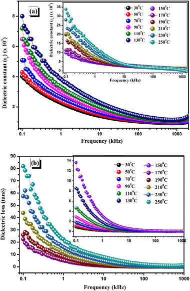 |
| | Fig. 5 (a) Frequency-dependent dielectric constant (εr) at different temperatures. (b) Frequency-dependent dielectric loss at various temperatures. | |
A reduction in the loss with increasing frequency can be observed in this dielectric property analysis. Surface charge effects provide a large value at low frequencies, while dipolar relaxation causes a significant decrease in dielectric loss (tanδ).33 An overall relaxation effect results from the oscillation of the applied electric field at higher frequencies, making the space charges react rapidly.34 CBFMO has remarkable dielectric features, as it reports a low loss tangent of tanδ = 9.0126 at 100 Hz and a high dielectric constant of εr = 4023.194 at room temperature.
4.2. Variation of dielectric constant and loss with temperature
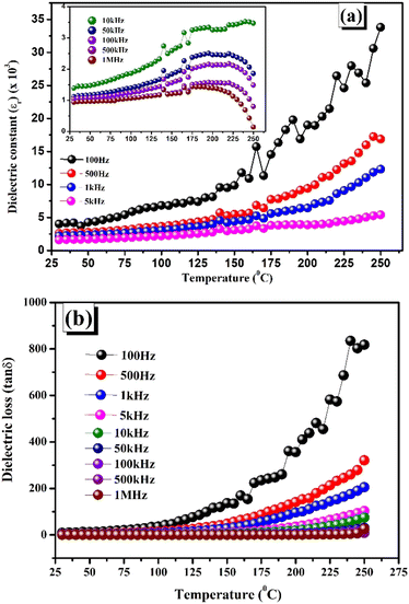
Fig. 6(a) and (b) demonstrate the temperature-varying dielectric constant (εr) and the dielectric loss (tanδ) for temperatures ranging from 50–300 °C across various frequencies, i.e., 100 Hz, 1 kHz, 10 kHz, 100 kHz, and 1 MHz. It is found that dielectric characteristics, including tangent loss and relative permittivity, increase with the temperature at all frequencies. It is found that dielectric characteristics, including tangent loss and relative permittivity increase with respect to the temperature at all frequencies. This might be explained by the material having several forms of polarization, especially dipolar polarization. At high temperatures (250 °C), a rapid increase in the dielectric permittivity and loss at the 100 Hz frequency could reflect the existence of oxygen vacancies and charges that have been triggered by thermal agitation.35–37 In the dielectric vs. temperature curve, there exists a little fluctuation in all the frequencies at approximately 170 °C. The low-temperature dielectric constant tends towards a lower and more stable value because the thermal energy is insufficient to move the B-site cations and because dipole alignment is difficult in the low-temperature state. At higher temperatures, the dielectric constant value went up because of the mobility of the thermally excited charge carriers.38 The underlying cause of the exceptionally high amount of tangent loss may be the polaron hopping process, which is generated by lattice vibration in materials at high temperatures.39 The relevance of CaBiFeMnO6 double perovskites for high-temperature devices is evidenced by the apparent drop in tanδ values across all temperatures.40
 |
| | Fig. 6 (a) Temperature-dependent dielectric constant. (b) Temperature-dependent tangent loss. | |
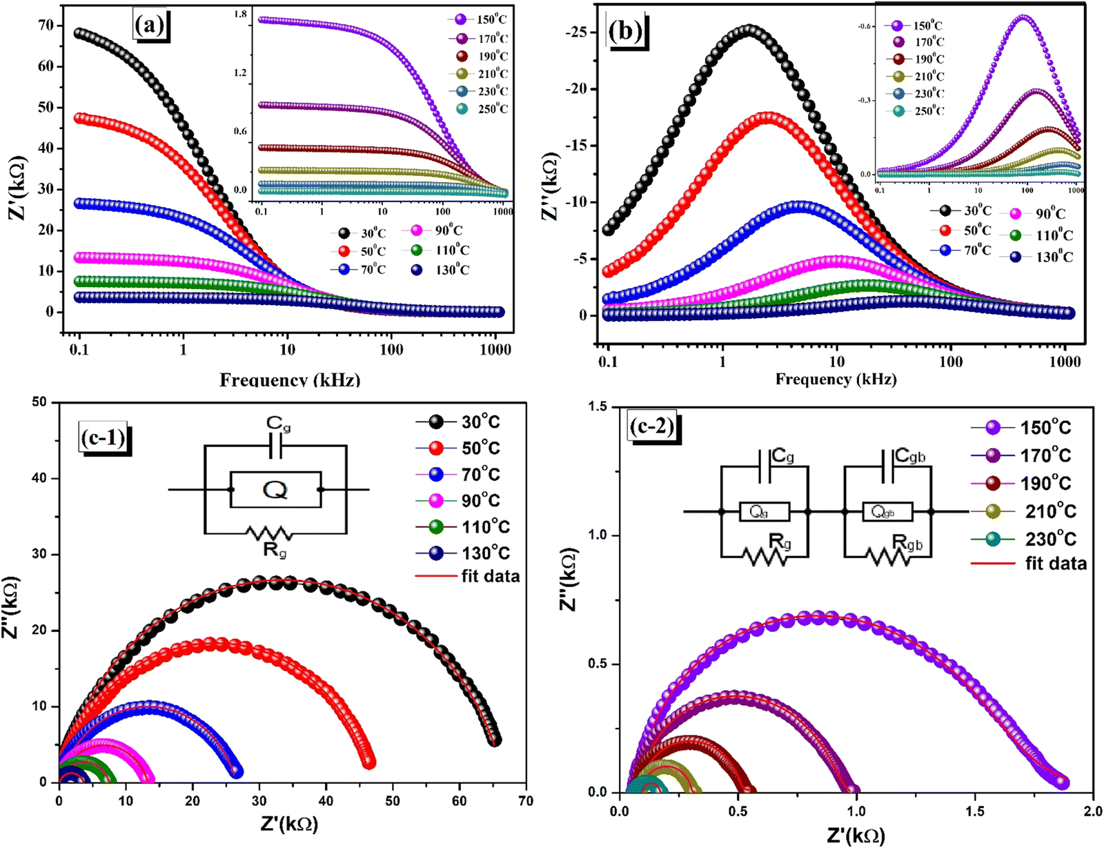
5. Complex impedance spectroscopy
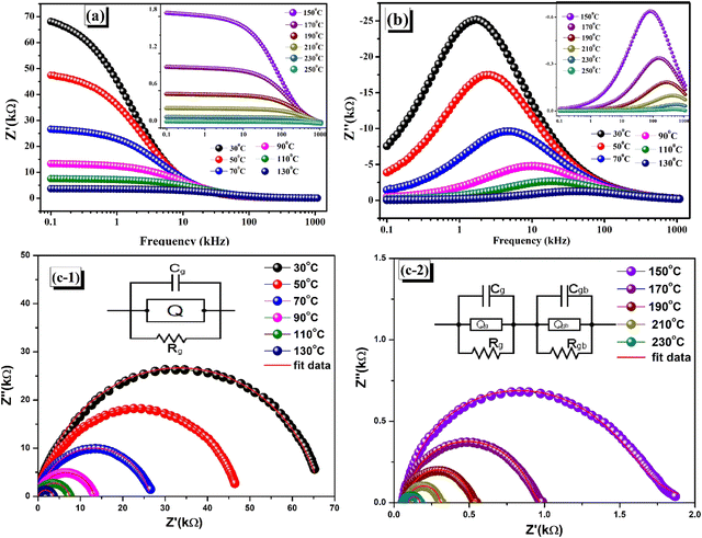
The transport and relaxation mechanisms of the oxide perovskites can be elucidated by complex impedance spectroscopy (CIS).41,42 In this elaborate procedure, alternating waves are applied to the specimen in the shape of a cylindrical pellet to evaluate the direction of the electric dipoles and the mobility of local charge carriers. A sophisticated, computer-monitored LCR analyzer then registers the data, guaranteeing precise and accurate measurements across an extensive frequency range, i.e., from 100 Hz to 1 MHz at various temperatures. For any given material, the angular frequency (ω)-dependent complex impedance Z*(ω) may be expressed in terms of the real part of the impedance Z′(ω) and the imaginary component of the impedance Z′′(ω).| | | Z*(ω) = Z′(ω) − jZ′′(ω) | (9) |
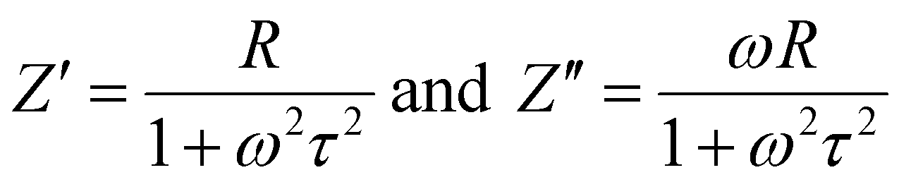
Three polarisation factors—grain–grain polarisation, grain boundary polarisation, and electrode polarization—observed at various frequency ranges mediate the semi-circular curves of the complex impedance spectra.43–46 The frequency varying impedance's real component (Z′) and imaginary part (Z′′) may be written as
| |  | (10) |
where
τ is the relaxation time, which includes the measured resistance (
R) and capacitance (
C) as
τ =
RC, and
ω is the angular frequency.
44 The frequency-dependent impedance is plotted for various temperatures as seen in
Fig. 7(a) and (b). A greater polarization in the ceramic at lower frequencies is evidenced, as indicated by a higher value.
47–49 Grain–grain interaction, grain boundary, and electrode interface are the three primary components that mediate the decrease in resistances that occur when the
Z′ and
Z′′ values abruptly fall at higher frequencies and temperatures.
22 The semiconducting behaviour of the synthesized specimen can be witnessed by the negative temperature coefficient of resistance (NTCR), which is correlated with the decrease in the impedance value when considering the real impedance for various temperatures.
 |
| | Fig. 7 (a) Frequency varying real impedance (Z′). (b) Frequency varying imaginary impedance (Z′′) at different temperatures. (c-1), (c-2) Z'–Z′′ (impedance Nyquist plots) at different temperatures. | |
5.1. Nyquist plot
An exceptionally effective and non-destructive method for analyzing the electrical response of ceramic materials to AC signals is impedance analysis. In order to explore the behavior of the ceramic compound, Fig. 7(c-1) and (c-2) depict Nyquist plots that show Z′ vs. Z′′. The experimental arcs were subjected to comparison with standard equivalent circuits using the ZSIMPWIN programme. Thus, it is possible to adequately comprehend the impacts of the grain and grain boundary effects on the specimen. For reliable findings, complex impedance plots are obtained at different temperatures in the frequency range of 100 Hz to 1 MHz. The phenomenon with the highest resistance is best illustrated by the Nyquist plot (Z′–Z′′).48 The depressed semicircles that are observed are indicative of dispersion in relaxation time and can be attributed to both the scattering of electromagnetic waves and differences in particle size.39 The impedance of the simulated electrical circuit with the ideal resistor (R) and capacitor (C) was compared with the experimental impedance data in this analytical approach. Up to 130 °C, the semi-circular arcs were matched to the parallel RQC circuit (Q = constant phase element), demonstrating the influence of the bulk grain. The resistance denotes the conductive route, while the capacitance indicates the polarisation of the space charge. Q = 1/(jωC)nRn−1 is the definition of the Q parameter, which may describe either a pure resistor (n = 0) or a pure capacitor (n = 1). In the upper range of the permitted temperature, both the grain and grain barrier effects were seen, and the optimal matching was determined by combining two parallel RQC–RQC circuits in series. The progressive reduction of the semicircular arc is caused by the diminishing frequency, because of both grain and grain boundary contributions over temperature.50–52 Thermal activation effectively stimulates the charge transport pathway in the intra-grain and grain border regions.53,54
6. Complex modulus spectroscopy
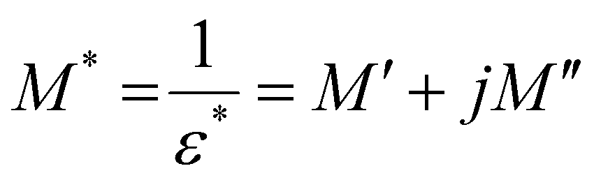
An essential technique for learning more about conductivity and relaxation mechanisms is electric modulus spectroscopy. The advantage is that it can remove the electrode polarisation effect that frequently occurs when measuring impedance.53–55| | 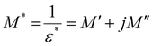 | (11) |
Here, the real part of the complex modulus (M′) and the imaginary part of the complex modulus (M′′) are defined as follows.
| | 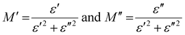 | (12) |
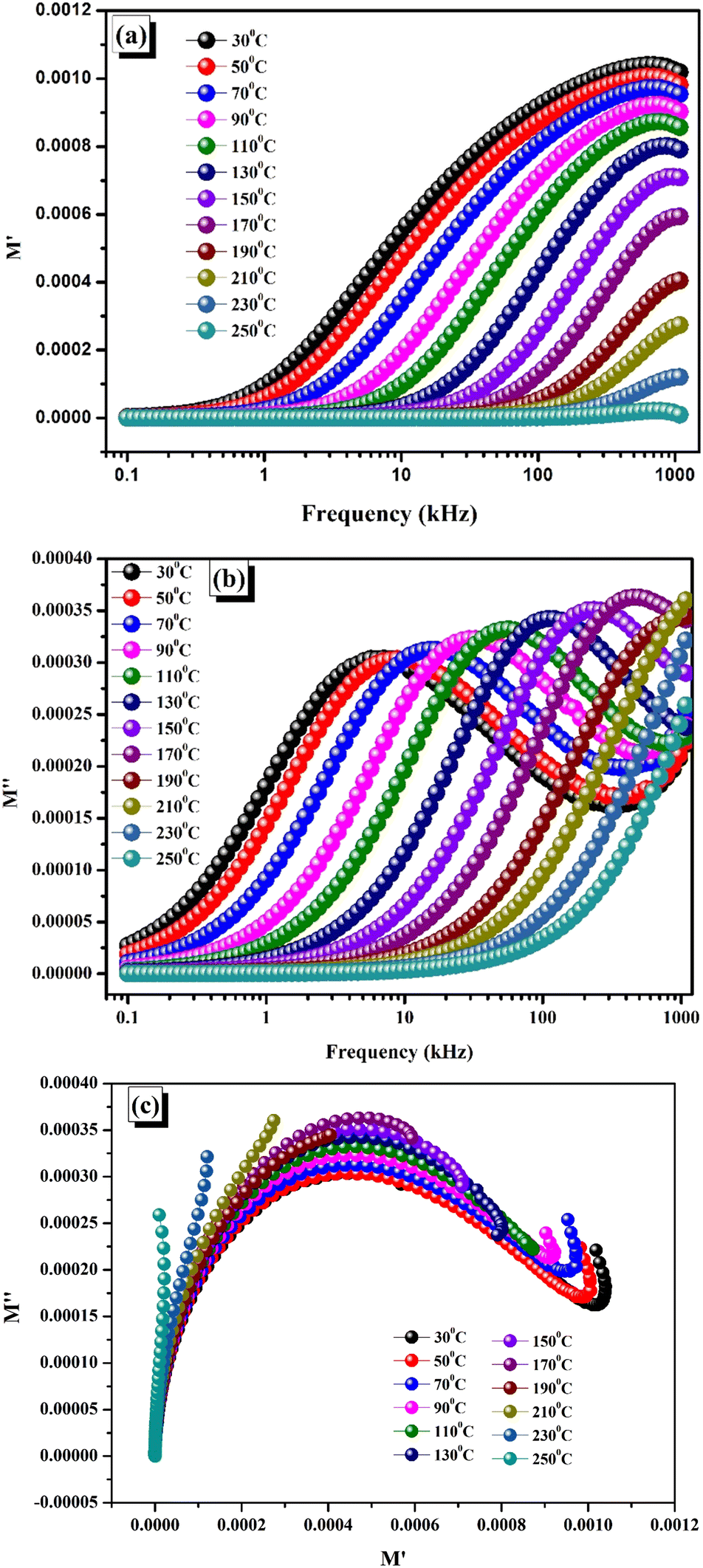
The frequency-dependent real and imaginary parts of the electrical modulus, or M′ vs. frequency and M′′ vs. frequency, are shown in Fig. 8(a) and (b).
 |
| | Fig. 8 (a) Variation of real modulus (M′) with frequency at different temperatures. (b) Variation of imaginary modulus (M′′) with frequency at different temperatures. (c) Variation of real modulus (M′) with imaginary modulus (M′′) at different temperatures. | |
The existence of short-range mobility among the charge carriers can account for the diminution in M′ at low frequencies and the increase in dispersion at higher frequencies. M′ at lower frequencies goes to zero. The absence of restoring forces brought on by the applied electric field affects this mobility.50,56 It is noteworthy that a constant reduction in the M′ values across all graphs is observed as the temperatures ascend until they finally intersect in the high-frequency areas, this pattern continues. Thus, the transfer of charge carriers across small distances is responsible for the conduction process. Moreover, the high-frequency merging of M′ provides proof that the processed sample does not exhibit electrode polarization.54 The apparent shift of the M′′ peaks towards higher frequencies as the temperature rises is indicative of the temperature-controlled relaxation process in the material, where the charge carriers are mostly confined to certain potential wells.57–60 The peak height of M′′ increased noticeably as the temperature increased. Ferroelectric materials often exhibit a reduction in capacitance with increasing temperature.45
Complex modulus analysis is an additional useful method for figuring out the electrical characteristics of the prepared specimen and interpreting the dynamic aspects and other features found in the sample. It also suppresses the electrode effect more. Fig. 8(c) illustrates the complex electric modulus spectrum in a temperature range of 30 °C to 250 °C. The real axis intercepts indicate the extent to which the grain and grain boundary contribute to the overall capacitance. Additionally, when the temperature rises, a shift in the modulus spectra is seen, which implies that the temperature-dependent capacitance value may also alter. The modulus spectra show asymmetrically shaped and flattened semicircular arcs whose centres do not lie on the abscissa (M′ axis), indicating non-Debye type dielectric relaxation; this type of curve is evocative of the temperature-dependent hopping mechanism for electric conduction.
7. Transport properties of CaBiFeMnO6
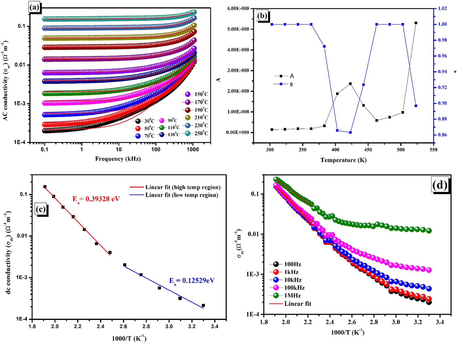
In order to comprehend the many physical aspects of dielectric/ferroelectric materials, such as their mechanical properties, optical qualities, or dielectric behaviour in response to electric impulses, it is essential to investigate their electrical conductivity. The controlled movement of charged particles in an electric field produces effective electrical conduction in dielectrics.24 The mechanism of conductivity in materials usually involves the hopping action of donor and acceptor carriers, depending on the temperature. Because of the low mobility of ionic charges, this mechanism is necessary for efficient conduction. The conductivity process in a dielectric sample is significantly impacted by an external alternating current field. Here, diffusion occurs among the mobile charge carriers, or weakly bound ions, and is a significant variable in increasing the total conductivity.21 Various methods are widely used to determine the characteristics of the AC conductivity, particularly with regard to changes that are based on temperature. The mechanisms that help us better understand the complicated behaviour of perovskite materials at different temperatures includes variable range hopping (VRH), small polaron hopping (SPH), quantum mechanical tunnelling (QMT), non-overlapping small polaron tunnelling (NSPT), and overlapping large polaron tunnelling (OLPT).61
7.1. Variation of AC conductivity with frequency
In terms of permittivity and angular frequency (ω), the expression for the AC conductivity (σac) is as follows.| | | σac = ωεrεotanδ | (13) |
In this case, εr and εo stand for the relative dielectric permittivity and absolute permittivity, respectively, while tanδ represents the tangent loss. The relationship between applied field frequency and electrical conductivity (σac) in the 30–250 °C range of temperatures is depicted in Fig. 9(a).
 |
| | Fig. 9 (a) AC conductivity as a function of frequency at various temperatures with Jonscher power law fitting. (b) DC conductivity vs. 1000/T. (c) Temperature-dependent s and A. (d) AC conductivity vs. 1000/T. | |
The significant increase in the σac, which is observed with both frequency and temperature, indicates the conduction phenomenon resulting from the temperature-dependent hopping activity of the charge carriers.28 The graph unambiguously indicates that, at all temperatures in the low-frequency range, the AC conductivity curves show a linear rise in frequency dependency. This suggests that conductivity and frequency have a steady and predictable connection. The boost in AC conductivity at lower frequencies can be attributed to the existence of interfacial or space charge polarisation as well as anomalies in the cation arrangement at nearby sites. These components support the increased electrical conductivity. The AC conductivity curves exhibit a characteristic pattern at high frequencies at all temperatures. Higher frequency mediated electrons exhibit a hopping process that results in this pattern, which is characterised by dispersion and saturation.62–64 Since localized charge carriers participate in this conduction process, polaron entities arise at places close by.64–66 The AC conductivity versus frequency plot shows a plateau and a dispersion. The plateau region indicates the presence of long-range DC conductivity at lower frequencies, while the dispersion zone highlights localised AC conductivity at higher frequencies. To further comprehend these areas, the Jonscher power law equation for angular frequency (ω = 2πf) and DC conductivity (σdc) may be stated as
where the power law exponent
s represents the degree of interaction between charges and the lattice structure, and the polarisation strength
A is given as a pre-exponential constant.
66 The graphical representation of the Jonscher law fitted in
Fig. 9(a) depicts the DC conductivity (
σdc), polarisation strength (
A), and power law exponent (
s) at multiple frequencies. Two linear zones can be observed when the DC conductivity is plotted against 1000/
T, as shown in
Fig. 9(b). These regions are then fitted to get the activation energy (
Ea) using the Arrhenius equation
| |  | (15) |
where
σ0 and
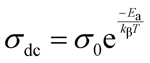
kβ represent the pre-exponential factor and Boltzmann constant, respectively.
67 The linearly fitted data was used to compute the two different activation energies 0.39328 eV and 0.12529 eV for the high temperature and low temperature domains, respectively.
In Fig. 9(c), s and A are plotted versus temperature. A correlated barrier hopping mechanism takes over in the conduction process when the value of s decreases with rising temperature. Conversely, if s grows with temperature, it suggests that the primary mechanism is small polaron conduction.67 It has been noticed that, when the temperature rises, for the given material, s starts to decrease, reaches a minimum, and then increases. Overlapping large polaron tunnelling (OLPT) is the most pertinent conduction mechanism in light of this tendency.67,68 Concurrently, the polarization parameter A state undergoes a reversal of direction and attains its peak value. The lowest value of s and the most significant value of A at the given temperature is prompted by the restricted range of correlating force amongst the charge carriers.45
7.2. Variation of AC conductivity with temperature
The inverse temperature-dependent AC conductivity (σac) varies with inverse temperature for a particular range of frequencies, as illustrated in Fig. 9(d). An extensive range of AC conductivity values at lower temperatures is observed from the plot. As the temperature rises, these values typically rise and converge towards higher temperatures. This temperature-dependent rise in conductivity suggests that the material under investigation has temperature-dependent hopping activity. The increasing pattern in conductivity (σac) is caused by thermally activated carriers.35 This finding indicates unequivocally that the compound exhibits a negative temperature coefficient of resistance (NTCR) and semiconducting properties. The activation energies for the provided frequencies were found using the Arrhenius equation and are listed in Table 4.
Table 4 Calculated activation energies for different frequencies
| S. no. |
Frequency (kHz) |
Activation energy (Ea) (eV) |
| 1 |
0.1 |
0.24944 |
| 2 |
1 |
0.24568 |
| 3 |
10 |
0.24642 |
| 4 |
100 |
0.22954 |
| 5 |
1000 |
0.17293 |
8.
I–V characteristic study
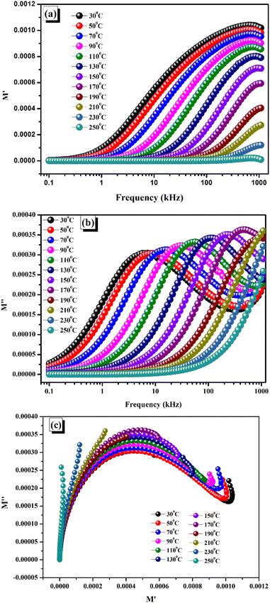
The correlation between current density (J) and applied electric field (E) at room temperature is shown in Fig. 10(a), where the noticeable nonlinearity in the I–V curve, which displays non-ohmic behaviour, supports the semiconducting properties.69 The relevance of the logarithmic function of the leakage current density (J) in relation to the applied electric field (E) is illustrated in Fig. 10(b). The upward trend in leakage current can be ascribed to the substantial function potential barrier. Since there is no potential barrier, the charge carriers in the material may readily spread out at low temperatures.21 With the increasing temperature, the hopping mechanism of the barrier is triggered and eventually results in leakage. The correlation between temperature and potential barrier indicates that charge carrier behaviour with regard to leakage is significantly influenced by this parameter. Fluctuations in temperature may have an impact on electron mobility and conductivity.69
 |
| | Fig. 10 (a) I–V characteristic plot, (b) logJ vs. E at various temperatures. | |
9. Magnetic property study
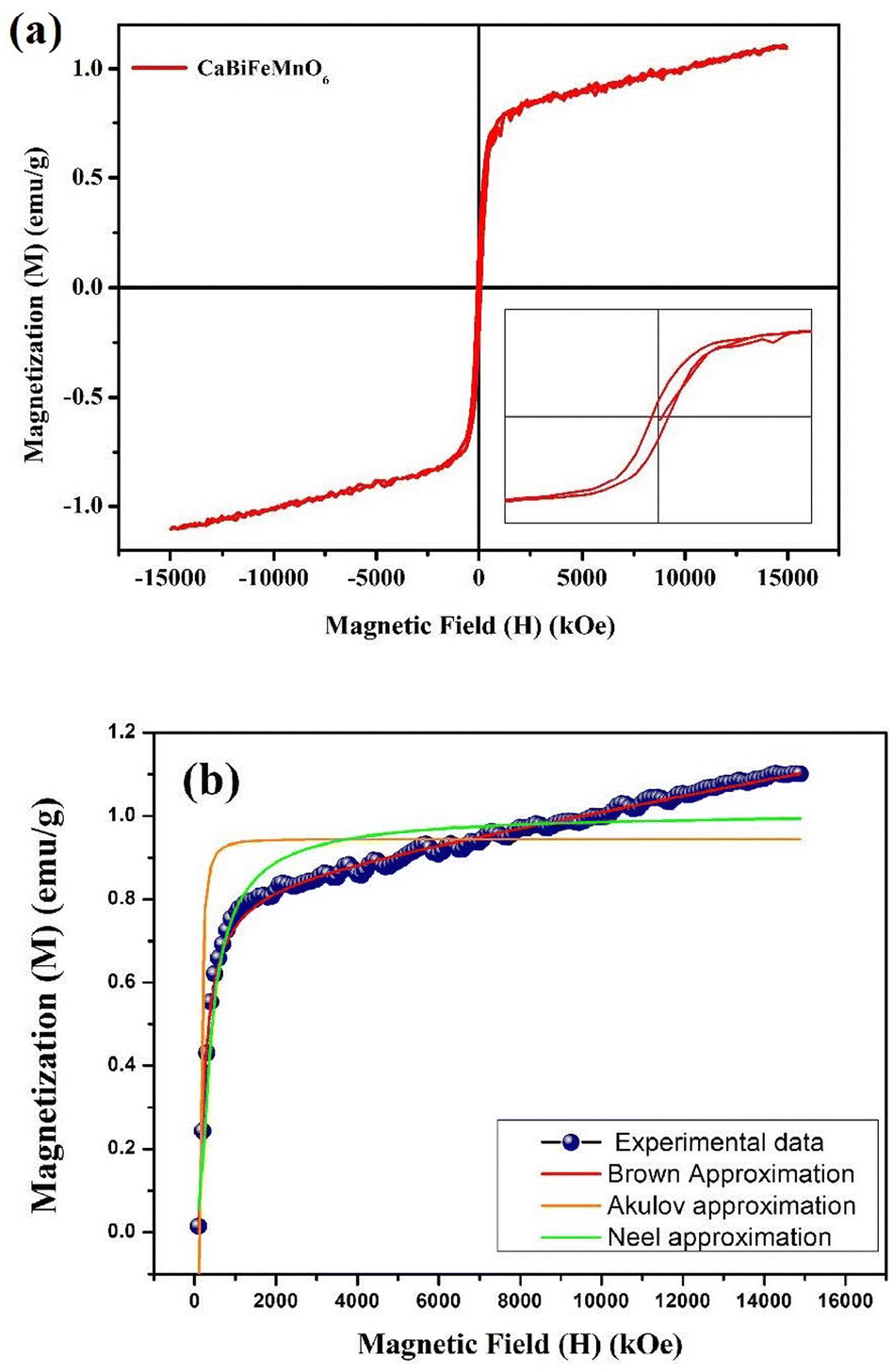
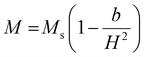
Due to the inclusion of two ferromagnetic cations at the B-site, the analysis of the magnetic behaviour of the material is accentuated. The magnetization potential of the prepared specimen is scrutinized through the magnetization (M) vs. applied magnetic field (H) to explore possible applications in different industrial aspects. The interaction of virtual electrons between two half-filled and one half-filled with completely filled or with empty orbitals satisfies the Goodenough–Kanamori rule concerning 180° super-exchange coupling and maintains the magnetic properties of the solid solution.70 The super-exchange interactions between two half-filled overlapped orbitals, which in turn participate in the spin exchange, regulate the antiferromagnetic behaviour of the materials.12,13 Two important features were introduced in the Mn-doped BiFeO3 material by the efficient maintenance of charge neutrality caused by the substitution of Mn4+ cations at the Fe3+ cationic site. First and foremost, this assists in the finding of oxygen locations. Second, it causes Fe3+ cations to be converted into Fe4+ cations. Fe3+ and Fe4+ cations together have the potential to behave ferromagnetically by increasing the magnetisation.71 The magnetization (M) vs. applied magnetic field (H) curves, which illustrate the magnetic moment vs. the applied magnetic field range from −15000 Oe to +15000 Oe, are displayed in Fig. 11. It was discovered that the base material's spatially modulated spin order may be effectively suppressed by substituting Ca at the A-cationic location. This leads to a non-zero net magnetization and a non-linear lossless M–H hysteresis loop with ferromagnetic response, as shown in the inserted image of the loop. Even at ambient temperature, this ceramic material displays a spectacular hysteresis loop with obvious signs of ferromagnetic characteristics. The large amount of ferromagnetic Fe dopant in the present compound and the dominance of the twofold exchange contact between the ferromagnetic cations (Fe/Mn3+–O–Fe/Mn4+) confirm the ferromagnetic property of CBFMO double perovskite.72 The ferromagnetic functionality of the material is demonstrated by the hysteresis loop, where the remnant magnetization (Mr) is found to be 0.149 emu g−1. However, the saturation magnetization (Ms) value is not evident from the figure. This often occurs in ferromagnets because of the influence of magnetocrystalline anisotropies and stress. The magnetocrystalline anisotropy from hysteresis loops is obtained by applying the law of approach to saturation (LAS).73 The variance of M–H in the higher field domain is explained by the law of approach to saturation (LAS), which can be illustrated by the following equation.| |  | (16) |
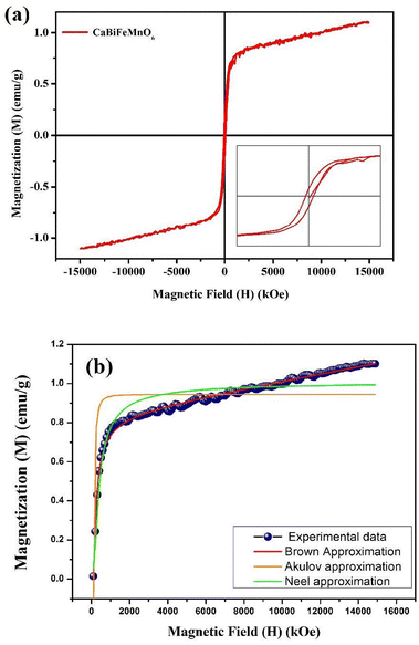 |
| | Fig. 11 (a) M–H hysteresis loop of CaBiFeMnO6. (b) Law of approach to saturation (LAS) plot. | |
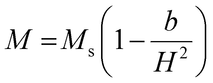
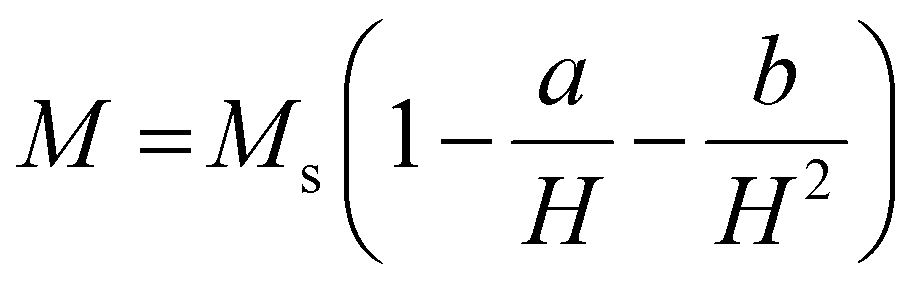
In this case, a/H stands for magnetic hardness, b/H2 for magnetocrystalline anisotropy, and χH for a term that resembles paramagnetism, and this equation corresponds to Brown's approximation. When fitting the present data to the above-mentioned approximation, we observed an increasing trend of magnetisation value that does not correspond to a saturation magnetization value. As the LAS approximation has several versions, the experimental data are compared to the other forms of approximation, i.e., the Akulov and Néel approximations, as shown in Fig. 11(b). The following equations were taken into consideration for these approximations.
| |  | (17) |
| |  | (18) |
Here, eqn (15) and (16) are the Akulov and Néel approximations, respectively, for LAS.73 From the fitted graph, it is evident that the experimental data does not follow Brown's approximation, but the other two approximations are approaching a saturation value at a certain magnetic field.
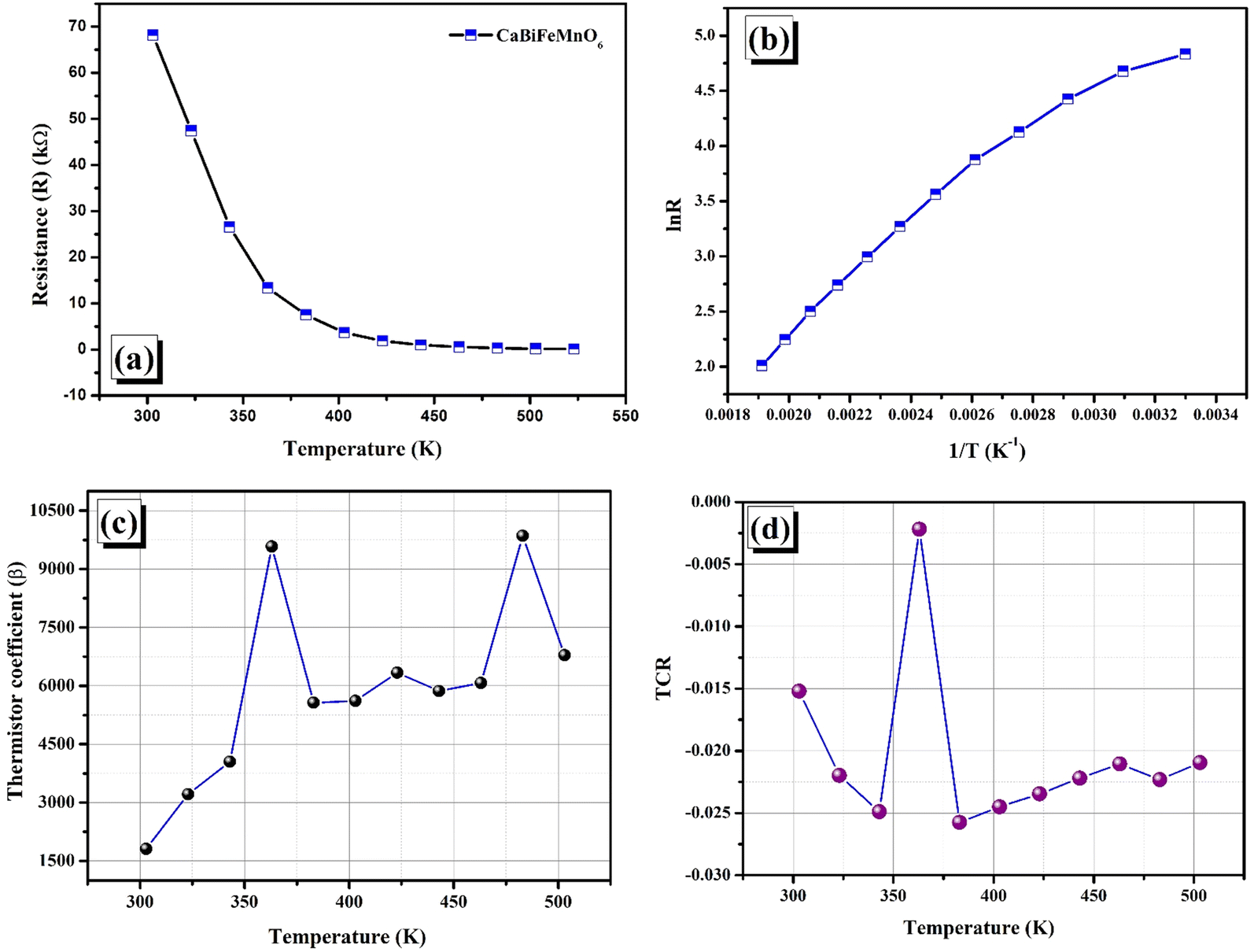
10. Response of resistance with respect to the temperature
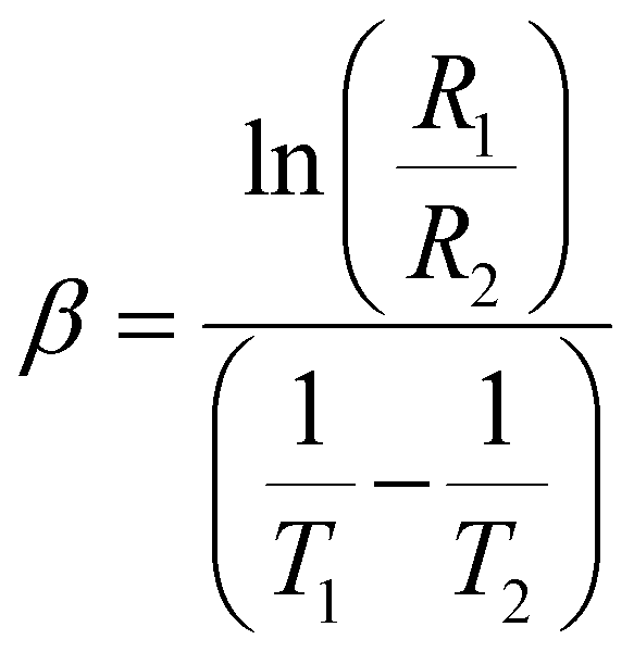
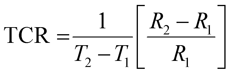
Because of the NTCR properties possessed by the material, it is feasible to create a sensor called a thermistor by examining how resistance changes with temperature.74,75 Our current analysis leans towards the second of the two thermistor principles: the positive temperature coefficient (PTC) thermistor and the negative temperature coefficient (NTC) thermistor. Fig. 12(a) illustrates the change in resistance within a certain temperature range of 300–550 K, while the variation of the logarithmic function of resistance (lnR), where R is the inverse of temperature (1/T), is displayed in Fig. 12(b). To have a thorough comprehension of thermistor functioning, it is necessary to examine many physical parameters, such as activation energy (Ea), thermistor constant (β), and sensitivity index (α). Through further examination of these ideas, we may gain a greater understanding of the underlying principle and operation by examining the mathematical relationships involved, which are Rτ = αexp(1/T) and logR = C + 1/T, where α and C are two constants.76 According to our experimental results, a linear correlation between the resistance in logarithmic form and the inverse of absolute temperature is required for the thermistor to operate as intended. The appropriate formulation to compute the temperature coefficient of resistance (TCR) and thermistor constant (β) can be expressed as| |  | (19) |
| |  | (20) |
where R1 and R2 correspond to the values of resistance at temperatures T1 and T2. For each set of temperatures, the corresponding thermistor constant and TCR are calculated and the relationship between the absolute temperature and the thermistor coefficient (β) is plotted in Fig. 12(c). The trend of β increasing with temperature supports the material's negative temperature coefficient (NTC) behaviour, indicating an excellent NTC type thermistor response.76,77 As shown in Fig. 12(d), the non-linear TCR temperature graph perfectly illustrates the significance for thermosensor applications. It is undisputed that the manufacture of NTC thermistors benefits greatly from larger thermistor constants and lower TCR values. For the specified temperature settings, the sensitivity factor (α), which is written as (−β/T2), is computed and displayed in Table 5. This demonstrates non-linear growth relative to the absolute temperature, making it suitable for thermosensor applications.21
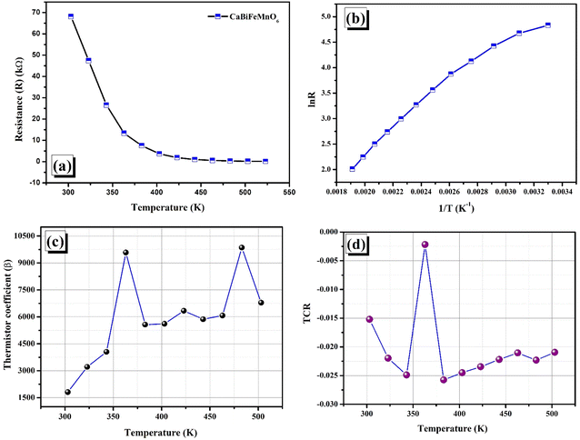 |
| | Fig. 12 (a) Change in resistance with temperature. (b) lnR versus 1/T, (c) thermistor constant (β) vs. temperature. (d) Change in the temperature coefficient of resistance (TCR) with temperature. | |
Table 5 Calculated sensitivity factors (α) for thermistor application
| Temperature (K) |
Sensitivity factor (α) |
| 323 |
−1.59518 |
| 348 |
−1.44766 |
| 373 |
−1.28995 |
| 398 |
−1.13645 |
| 423 |
−1.01192 |
| 448 |
−0.8837 |
| 473 |
−0.77277 |
| 498 |
−0.67577 |
| 523 |
−0.59154 |
| 548 |
−0.5179 |
11. Conclusion
A cost-effective solid-state synthesis was employed to produce the new polycrystalline double perovskite CaBiFeMnO6, altering its physical characteristics by the cationic substitution of different elements at both the A and B sites. The orthorhombic phase was confirmed by Rietveld refinement analysis. The mean crystalline size was found to be 69.57 nm, and the field emission scanning electron micrograph reveals it has considerable porosity and an uneven distribution of grains on its surface. The impedance evaluation in a certain temperature range for a particular electric field validated the exclusive negative temperature coefficient of resistance (NTCR) behaviour which was corroborated by the dielectric property analysis. Because of its high room temperature dielectric constant of 4093 and low tangent loss, CBFMO has potential use in a variety of energy storage devices, including supercapacitors. For use as a NTC thermistor, the thermistor constant (β) and temperature coefficient of resistance (TCR) were calculated to display the NTCR characteristic. The M–H hysteresis loop proves that the Ca-substituted Bi2FeMnO6 is ferromagnetic.
Data availability
Some of the data generated during this study are included in this article. The rest datasets generated during the current study are available from the corresponding author on reasonable request.
Conflicts of interest
The authors declare that they have no known competing financial interests or personal relationships that could have appeared to influence the work reported in this paper. We declare that the manuscript is new and has not been submitted anywhere for publication. In addition to the above, we have no conflicts of interest with anybody except Paweł E. Tomaszewski.
Acknowledgements
We declare that this study did not receive any grants, money, or other support.
References
- H. Zhang, A. Chang and C. Peng, Microelectron. Eng., 2011, 88, 2934–2940 CrossRef CAS.
- X. Xiong, J. Xu, P. Zhao, L. Wang, L. Bian, F. Xu, J. Zhang and A. Chang, Ceram. Int., 2014, 40, 10505–10510 CrossRef CAS.
- H. Chen, G. Wei, X. Liang, P. Liu, Y. Xi and J. Zhu, Catal. Sci. Technol., 2020, 10, 5829–5839 RSC.
- F. Guan, Z. Dang, X. Chen, S. Huang, J. Wang, X. Cheng and Y. Wu, J. Alloys Compd., 2021, 871, 159269 CrossRef CAS.
- M. C. Knapp and P. M. Woodward, J. Solid State Chem., 2006, 179, 1076–1085 CrossRef CAS.
- G. King and S. Garcia-Martin, Inorg. Chem., 2019, 58, 14058–14067 CrossRef CAS PubMed.
- Q. Liu, J. Guo, M. Fan, Q. Zhang, S. Liu, K.-L. Wong, Z. Liu and B. Wei, J. Mater. Chem. C, 2020, 8, 2117–2122 RSC.
- K. Ji, J. R. Bedward, Q. Li, P. Manuel, C. Ritter and J. P. Attfield, Chem. Commun., 2023, 59, 6371–6374 RSC.
- T. Ahmed, A. Chen, D. A. Yarotski, S. A. Trugman, Q. Jia and J.-X. Zhu, APL Mater., 2017, 5, 035601 CrossRef.
- M. Qu, X. Ding, Z. Shen, M. Cui, F. E. Oropeza, G. Gorni, V. A. de la Peña O’Shea, W. Li, D.-C. Qi and K. H. L. Zhang, Chem. Mater., 2021, 33, 2062–2071 CrossRef CAS.
- L. Sun, Y.-W. Fang, J. He, Y. Zhang, R. Qi, Q. He, R. Huang, P. Xiang, X.-D. Tang and P. Yang, J. Mater. Chem. C, 2017, 5, 5494–5500 RSC.
- Z. Pei, K. Leng, W. Xia, Y. Lu, H. Wu and X. Zhu, J. Magn. Magn. Mater., 2020, 508, 166891 CrossRef CAS.
- P. Song, Z. Pei, H. Wu, Y. Lu, W. Xia and X. Zhu, Adv. Mater. Lett., 2019, 10, 874–879 CrossRef CAS.
- P. Liu, Z. X. Cheng, Y. Du, L. Y. Feng, H. Fang, X. L. Wang and S. X. Dou, J. Appl. Phys., 2013, 113, 17D904 CrossRef.
- Y. Du, Z. X. Cheng, S. X. Dou, X. L. Wang, H. Y. Zhao and H. Kimura, Appl. Phys. Lett., 2010, 97, 122502 CrossRef.
- R. Das and R. N. P. Choudhary, Solid State Sci., 2019, 87, 1–8 CrossRef CAS.
- T. A. Para and S. K. Sarkar, Adv. Ceram. Mater., 2021, 10, 16 Search PubMed.
- V. D. Mote, Y. Purushotham and B. N. Dole, J. Theor. Appl. Phys., 2012, 6, 1–8 CrossRef.
- D. Nath, F. Singh and R. Das, Mater. Chem. Phys., 2020, 239, 122021 CrossRef CAS.
- S. Mishra, R. N. P. Choudhary and S. K. Parida, Ceram. Int., 2022, 48, 17020–17033 CrossRef CAS.
- B. Mohanty, S. Bhattacharjee, N. C. Nayak, R. K. Parida and B. N. Parida, Mater. Sci. Semicond. Process., 2021, 128, 105720 CrossRef CAS.
- B. N. Parida, P. Biswal, S. Behera, R. K. Parida and R. Padhee, J. Mater. Sci.: Mater. Electron., 2020, 31, 6097–6108 CrossRef CAS.
- L. Sahoo, B. N. Parida, N. C. Nayak and R. K. Parida, J. Mater. Sci.: Mater. Electron., 2023, 34, 1019 CrossRef CAS.
- B. Mohanty, B. N. Parida and R. K. Parida, J. Mater. Sci.: Mater. Electron., 2019, 30, 9211–9218 CrossRef CAS.
- B. N. Parida, R. K. Parida and A. B. Panda, J. Alloys Compd., 2017, 696, 338–344 CrossRef CAS.
- W. Hu, T. Li, X. Liu, D. Dastan, K. Ji and P. Zhao, J. Alloys Compd., 2020, 818, 152933 CrossRef CAS.
- S. A. Dar, G. Murtaza, T. Zelai, G. Nazir, H. Alkhaldi, H. Albalawi, N. A. Kattan, M. Irfan, Q. Mahmood and Z. Mahmoud, Colloids Surf., A, 2023, 664, 131145 CrossRef CAS.
- L. Sahoo, B. Mohanty, B. N. Parida, N. C. Nayak and R. K. Parida, Mater. Sci. Eng., B, 2023, 294, 116561 CrossRef CAS.
- N. Nazir and M. Ikram, J. Mater. Sci.: Mater. Electron., 2020, 31, 23002–23011 CrossRef CAS.
- S. Abass, A. Bagri and K. Sultan, J. Alloys Compd., 2023, 930, 167463 CrossRef CAS.
- Y. Kumar, J. Pal, P. S. Malhi and R. Kumar, J. Adv. Dielectr., 2020, 10, 2050032 CrossRef CAS.
-
M. Chanda, Science of Engineering Materials: Structure of Matter, 1st edn, 1981, vol. 1 DOI:10.1007/978-1-349-06051-1.
- L. Sahoo, B. N. Parida, R. K. Parida, R. Padhee and A. K. Mahapatra, Inorg. Chem. Commun., 2022, 146, 110102 CrossRef CAS.
- A. Bendahhou, K. Chourti, M. Loutou, S. El Barkany and M. Abou-Salama, RSC Adv., 2022, 12, 10895–10910 RSC.
- B. Mohanty, S. Bhattacharjee, S. N. Sarangi, N. C. Nayak, R. K. Parida and B. N. Parida, J. Alloys Compd., 2021, 863, 158060 CrossRef CAS.
- B. Mohanty, B. N. Parida and R. K. Parida, Ceram. Int., 2020, 46, 16502–16509 CrossRef CAS.
- D. Tlili, S. Hcini, A. Triki, S. Khadraoui, S. Zemni and M. Oumezzine, J. Supercond. Novel Magn., 2016, 29, 227–235 CrossRef CAS.
- D. K. Pradhan, S. Kumari, V. S. Puli, P. T. Das, D. K. Pradhan, A. Kumar, J. F. Scott and R. S. Katiyar, Phys. Chem. Chem. Phys., 2017, 19, 210–218 RSC.
- E. K. Abdel-Khalek, E. A. Mohamed, S. M. Salem and I. Kashif, J. Non-Cryst. Solids, 2018, 492, 41–49 CrossRef CAS.
- M. Amin, H. M. Rafique, M. Yousaf, S. M. Ramay and S. Atiq, J. Mater. Sci.: Mater. Electron., 2016, 27, 11003–11011 CrossRef CAS.
- S. Khadhraoui, A. Triki, S. Hcini, S. Zemni and M. Oumezzine, J. Alloys Compd., 2013, 574, 290–298 CrossRef CAS.
- R. Das and R. N. P. Choudhary, Process. Appl. Ceram., 2019, 13, 1–11 CrossRef CAS.
- S. Hcini, S. Khadhraoui, A. Triki, S. Zemni, M. Boudard and M. Oumezzine, J. Supercond. Novel Magn., 2014, 27, 195–201 CrossRef CAS.
- A. K. Panda, L. Sahoo, R. Chakravarty, N. C. Nayak, R. K. Parida, B. N. Parida and R. Dutta, Appl. Phys. A: Mater. Sci. Process., 2021, 127, 1–11 CrossRef.
- S. Sen, R. K. Parida and B. N. Parida, Phys. B, 2023, 650, 414559 CrossRef CAS.
- N. Saikia, R. Chakravarty, S. Bhattacharjee, R. L. Hota, R. K. Parida and B. N. Parida, Mater. Sci. Semicond. Process., 2022, 151, 106969 CrossRef CAS.
- S. G. Infantiya, A. Aslinjensipriya, R. S. Reena, K. J. Pious, P. Sivakumar, C. J. Raj and S. J. Das, J. Mater. Sci.: Mater. Electron., 2023, 34, 1994 CrossRef CAS.
- A. Prasad, R. K. Mishra, K. P. Chandra and K. Prasad, Process. Appl. Ceram., 2018, 12, 383–393 CrossRef CAS.
- R. Chakravarty, R. K. Parida and B. N. Parida, Appl. Phys. A: Mater. Sci. Process., 2022, 128, 647 CrossRef CAS.
- J. Wang, H. Zhang, D. Xue and Z. Li, J. Phys. D: Appl. Phys., 2009, 42, 235103 CrossRef.
- A. Bendahhou, K. Chourti, F. Chaou, I. Jalafi, S. El Barkany and M. Abou-Salama, Mater. Res. Bull., 2023, 165, 112319 CrossRef CAS.
- M. Jebli, C. Rayssi, J. Dhahri and K. Khirouni, Appl. Phys. A: Mater. Sci. Process., 2020, 126, 1–16 CrossRef.
- R. Roy and A. Dutta, Ceram. Int., 2021, 47, 15732–15742 CrossRef CAS.
- D. L. Rocco, A. A. Coelho, S. Gama and M. de C. Santos, J. Appl. Phys., 2009, 42, 055002 Search PubMed.
- K. L. Routray and D. Behera, J. Mater. Sci.: Mater. Electron., 2018, 29, 14248–14260 CrossRef CAS.
- L. Sahoo, S. Sahoo, R. Chakravarty, N. Saikia, B. N. Parida and R. K. Parida, J. Inorg. Organomet. Polym. Mater., 2023, 1–16 Search PubMed.
- S. K. Barik, R. N. P. Choudhary and P. K. Mahapatra, Appl. Phys. A: Mater. Sci. Process., 2007, 88, 217–222 CrossRef CAS.
- P. Gogoi, P. Srinivas, P. Sharma and D. Pamu, J. Electron. Mater., 2016, 45, 899–909 CrossRef CAS.
- I. Coondoo, N. Panwar, A. Tomar, A. K. Jha and S. K. Agarwal, Phys. B, 2012, 407, 4712–4720 CrossRef CAS.
- K. L. Routray, S. Saha and D. Behera, Appl. Phys. A: Mater. Sci. Process., 2019, 125, 328 CrossRef CAS.
- F. A. Abdel-Wahab, H. M. Maksoud and M. F. Kotkata, J. Phys. D: Appl. Phys., 2005, 39, 190 CrossRef.
- M. Z. Halizan and Z. Mohamed, Materials, 2022, 15, 4363 CrossRef CAS PubMed.
- B. Mohanty, S. Bhattacharjee, R. K. Parida and B. N. Parida, Mater. Today: Proc., 2021, 35, 91–93 CAS.
- M. Shakir, B. K. Singh, R. K. Gaur, B. Kumar, G. Bhagavannarayana and M. A. Wahab, Chalcogenide Lett., 2009, 6, 655–660 CAS.
- S. Aydi, S. Chkoundali, A. Oueslati and A. Aydi, RSC Adv., 2023, 13, 20093–20104 RSC.
- K. I. Nassar, M. Slimi, N. Rammeh, A. Bouhamed, A. Njeh and O. Kanoun, J. Mater. Sci.: Mater. Electron., 2021, 32, 24050–24057 CrossRef CAS.
- A. ur Rahman, M. A. Rafiq, S. Karim, K. Maaz, M. Siddique and M. M. Hasan, J. Phys. D: Appl. Phys., 2011, 44, 165404 CrossRef.
- A. K. Roy, A. Singh, K. Kumari, K. Amar Nath, A. Prasad and K. Prasad, Int. Scholarly Res. Not., 2012, 2012, 854831 Search PubMed.
- S. S. Hota, D. Panda and R. N. P. Choudhary, Solid State Ionics, 2023, 399, 116313 CrossRef CAS.
- S. Sahoo, S. Mishra, L. Sahoo, B. N. Parida, L. Biswal and R. K. Parida, Ceram. Int., 2024, 50, 20011–20025 CrossRef CAS.
- A. D. Sharma and H. B. Sharma, Integr. Ferroelectr., 2019, 203, 81–90 CrossRef CAS.
- R. Sivasamy, P. Venugopal and R. Espinoza-González, Mater. Today Commun., 2020, 25, 101603 CrossRef CAS.
- R. Chakravarty, U. Das, R. K. Parida and B. N. Parida, J. Alloys Compd., 2023, 968, 171761 CrossRef CAS.
- S. Sahoo, S. K. S. Parashar and S. M. Ali, J. Adv. Ceram., 2014, 3, 117–124 CrossRef CAS.
- P. Mallick, S. K. Satpathy and B. Behera, Bull. Mater. Sci., 2022, 45, 198 CrossRef CAS.
- D. Panda, S. S. Hota and R. N. P. Choudhary, Mater. Sci. Eng., B, 2023, 296, 116616 CrossRef CAS.
- S. S. Hota, D. Panda and R. N. P. Choudhary, J. Mater. Sci.: Mater. Electron., 2023, 34, 900 CrossRef CAS.
|
| This journal is © The Royal Society of Chemistry 2024 |
Click here to see how this site uses Cookies. View our privacy policy here. 
 Open Access Article
 This Open Access Article is licensed under a Creative Commons Attribution-Non Commercial 3.0 Unported Licence
 b,
B. N.
Parida
c and
R. K.
Parida
b,
B. N.
Parida
c and
R. K.
Parida