
 Open Access Article
 This Open Access Article is licensed under a Creative Commons Attribution-Non Commercial 3.0 Unported Licence
Unravelling the polarity preference and effects of the electrode layer on wurtzite aluminum nitride for piezoelectric applications†
Zicong Marvin
Wong
,
Gang
Wu
 and
Ramanarayan
Hariharaputran
*
and
Ramanarayan
Hariharaputran
*
Institute of High Performance Computing (IHPC), Agency for Science, Technology and Research (A*STAR), 1 Fusionopolis Way, #16-16 Connexis, Singapore 138632, Republic of Singapore. E-mail: hariharaputran@ihpc.a-star.edu.sg
First published on 26th February 2024
Abstract
Aluminum nitride (AlN) is a promising material for electromechanical and optoelectronic applications due to its exceptional properties. The stability and control of the polarity of AlN surfaces, as well as the interactions between AlN and electrode layers, are critical for optimizing device performance. In this study, we investigate the properties of electrode layers on AlN slabs and their impact on the stability and polarity preferences of AlN surfaces. Using first principles simulations, we calculate the formation energies of various electrode layers on AlN slabs and analyze the resulting trends. Additionally, we examine the Bader charges of the electrode layers to gain insights into the nature of the interface interactions. Our findings reveal that the interaction between the electrode layer and the AlN slab is thermodynamically favorable and is mainly electrostatic or ionic in nature. The preferred stacking sequence of the electrode layer elements on Al-polar AlN slabs aligns with the overall wurtzite structure of the AlN slabs, minimizing lattice distortion and destabilization. The variation in the Born effective charge of the interfacial atoms on AlN slabs with electrode layer elements of different electronegativities could impact the interface polarization and piezoelectric properties. By considering electronegativity or Bader charges of the electrodes, the design of stable electrodes on AlN slabs with preferred polarity can be achieved. This study provides valuable insights into the design and optimization of AlN-based electronic and piezoelectric devices.
1. Introduction
Aluminum nitride (AlN) with its wurtzite crystalline structure holds significant potential for advanced electromechanical and optoelectronics devices. In particular, its wide band gap, thermal stability, high acoustic velocity, and excellent piezoelectric properties make it an appealing material for use in high-power electronic devices, sensors, and radio frequency (RF) acoustic devices like resonators.1–4 The non-centrosymmetric nature of wurtzite AlN gives rise to polarization along the c-axis, resulting in either the Al- or N-polarity AlN film or slab (Fig. 1). While significant efforts have been dedicated to improving the piezoelectric response through alloying or doping,5–7 the control of polarity is especially vital for the design of high-performance devices, such as thin film bulk acoustic wave (BAW) resonators, since different polarities can affect the piezoelectric properties and ultimately impact their operation performance.8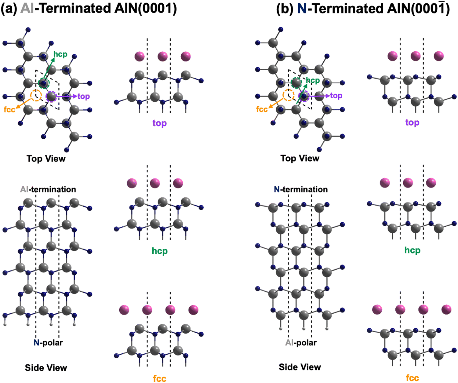 | ||
Fig. 1 Structural configurations of (a) Al-terminated AlN(0001) and (b) N-terminated AlN(000![[1 with combining macron]](https://www.rsc.org/images/entities/char_0031_0304.gif) ) slab model. The three possible interfacial stacking sequences for the electrode layer atoms are also shown. The blue, grey, pink, and white spheres correspond to the N, Al, electrode layer, and pseudo-H atoms, respectively. ) slab model. The three possible interfacial stacking sequences for the electrode layer atoms are also shown. The blue, grey, pink, and white spheres correspond to the N, Al, electrode layer, and pseudo-H atoms, respectively. | ||
Fabrication of AlN films is usually carried out via reactive sputtering deposition which permits deposition onto substrates at low cost and relatively low temperatures of 300 °C.9 However, controlling the polarity of AlN films is challenging due to their sensitivity towards various sputtering deposition conditions, such as (1) the surface oxidation state of the electrode whereby the oxidized Ru metal surface reverses the polarity of AlN from N- to Al-polarity;10 (2) the presence of residual oxygen in the chamber which not just inverts the polarity of AlN from Al- to N-polar on the Si substrate, but also results in deterioration in crystallinity of deposited AlN as well as reduction in piezoelectric performance;11 (3) the cathode power and sputtering pressure whereby Al-polar AlN is preferentially deposited at high cathode power and low sputtering pressure;8,12 and even (4) the thickness of the deposited AlN film which arises from the competition between an Al-polar template and a deposition process that favors N-polar films, leading to a polarity transition once a certain film thickness is achieved.13 Despite the significance of polarity control in optimizing the performance of AlN-based devices, the existing body of research is still limited and particularly restricted to experimental studies in comprehensively addressing the intricate interplay of factors influencing polarity preferences. Moreover, the rationale behind the observed polarity preferences for different electrodes remains relatively unexplored in the current literature. Understanding and controlling these factors are crucial for achieving the desired polarity alignment and optimizing the performance of AlN-based devices.
In this study, we investigate the properties of electrode layers on AlN slabs and their influence on the stability and polarity preferences of AlN surfaces via first principles simulations. By calculating and analyzing the formation energy of electrode layers and examining Bader charges, we reveal the thermodynamically favorable interaction between the electrode layer and AlN slabs, primarily driven by electrostatic or ionic forces. We find that the top interfacial stacking sequence is the preferred configuration for most electrode layer elements on Al-polar AlN slabs, minimizing lattice distortion and ensuring interfacial structural continuation. In addition, we observe that the variation in the Born effective charge of the interfacial Al atoms on N-polar AlN slabs, influenced by electrode layer elements with different electronegativities, can impact the interface polarization and piezoelectric properties of the N-polar AlN slabs.
While exploring these intricacies, our study draws parallels with the trends and studies on two-dimensional (2D) piezoelectric materials, a field of growing interest.14–16 Although 2D materials present fascinating possibilities, our focus on AlN slabs provides insights into the interface interactions, offering analogies to 2D stacked heterostructures.17 Our findings are particularly pertinent as they contribute to the fundamental understanding of polarity preferences and interface behavior, advancing the design and optimization of AlN-based electronic and piezoelectric devices. These insights can be instrumental in guiding further research into the development of stable interfaces with preferred polarities for AlN slabs, with considerations of electronegativity or Born effective charges of the electrode layers. This knowledge holds promise for the enhancement of AlN-based devices, contributing to advancements in high-power electronics, sensors, and acoustic resonators.
2. Methodology
Density functional theory (DFT) calculations18 were performed using the Perdew, Burke, and Ernzerhof exchange correlation based on the generalized gradient approximation (PBE-GGA)19,20 as implemented in the Vienna ab initio Simulation Package (VASP).21,22 The projector augmented wave (PAW)23 was utilized to describe the electron–ion interactions with plane-wave cutoffs set to 500 eV. To account for possible van der Waals interactions between surfaces and interfaces, the DFT-D3 dispersion corrections according to Grimme et al. were considered.24 Relaxation of the atomic coordinates were carried out in spin-unrestricted calculations until the calculated Hellmann–Feynman forces were less than 0.001 eV Å−1 and energy tolerance of 10−6 eV. Γ-centered Monkhorst–Pack (MP) k-point meshes25 with k-point density of approximately 20 k-points per Å−1 were used for Brillouin zone sampling, while finer 40 k-points per Å−1 meshes were implemented in the electronic density-of-states (DOS) calculations.The validation of our calculation method was carried out by calculating the lattice constants of bulk wurtzite aluminum nitride (w-AlN) with the hexagonal P63mc space group which yielded lattice constants of a = b = 3.114 Å and c/a = 1.603, in good agreement with the experimental value (a = 3.110 Å and c/a = 1.601)26 and previous calculation results.27
This was followed by modeling of the AlN Al-terminated (0001) and N-terminated (000) surface as slabs with a vacuum region of at least 20 Å between two consecutive slabs. The slab consisted of six AlN bilayers, with the lower four bilayers fixed for simulating the bulk phase during structural optimization. Pseudo-H atoms with fractional charges of 0.75 and 1.25 were employed to terminate the dangling bonds of N and Al respectively at the bottom to prevent unphysical charge transfer and to decouple the surfaces of the slab.28 The upper two bilayers and electrode layer were allowed to relax. For both Al- and N-terminated surfaces, there are three possible interfacial stacking sequences for the electrode layer, which differ in the position of the electrode layer atoms with respect to the AlN lattice slab, i.e., top, hcp (hexagonal close-packed), and fcc (face-centered cubic) sequences as illustrated in Fig. 1. The top sequence describes the electrode layer atoms located directly above the surface Al or N atoms. The hcp sequence describes the electrode layer atoms located directly above the N or Al atoms on the second uppermost layer. Finally, the fcc sequence describes the electrode layer atoms located in the three-fold hollow site not directly above any Al and N atoms of the AlN lattice slab. 37 different elements, C, Al, Si, Sc, Ti, V, Cr, Mn, Fe, Co, Ni, Cu, Zn, Ga, Ge, Y, Zr, Nb, Mo, Ru, Rh, Pd, Ag, In, Sn, Sb, Hf, Ta, W, Re, Os, Ir, Pt, Au, Hg, Pb, and Bi, were employed as the electrode layer atoms, which led to a total of 222 interface systems being investigated. These elements were selected as they are rather commonly used metals or semiconductors, relatively air or water stable, not overly toxic nor radioactive.
Our convergence tests for an optimal number of AlN layers for both Al- and N-terminated surface and electrode layers, as well as optimal vacuum density for the Bader charge determination, are included in the ESI.†
3. Results and discussion
3.1. Surface investigation of bare Al- and N-terminated aluminum nitride (AlN) slabs
Understanding the surface properties of bare Al- and N-terminated AlN slabs is crucial for gaining insights into their interactions with the electrode layers. To determine the surface energy γ and describe surface stability, we employ an expression derived and modified from Razia et al.:29 | (1) |
) surface energies of the AlN slabs were calculated to be 245.9 and 236.6 meV Å−2, respectively. The similarity in the magnitude of the surface energies suggest that the observation of preferred Al- or N-polarity are only marginally influenced by the stability of the Al- or N-terminated surfaces.30,31
Furthermore, ab initio calculations are used to determine the electronic structures of the Al- and N-terminated AlN slabs. Fig. 2 illustrates the layer-by-layer electronic partial density-of-states (pDOS), contour maps of electron density difference, and Bader analyses32–35 of the Al- and N-terminated AlN slabs. The pDOS of the bulk region (away from the surface) of the AlN slabs exhibits a semiconducting nature with band gaps, along with high ionicity and charge neutrality. The N atoms carry a negative charge of 2.35 e per N, while the Al atoms possess a corresponding loss of 2.35 e per Al, consistent with previously calculated bulk AlN.36
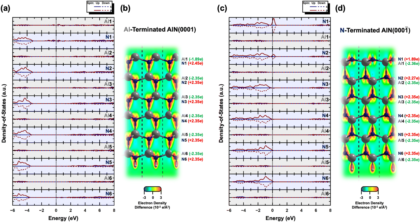 | ||
Fig. 2 (a) Layer-by-layer electronic partial density-of-states (pDOS) and (b) optimized structure of the Al-terminated AlN(0001) slab, as well as (c) layer-by-layer electronic pDOS and (d) optimized structure of the N-terminated AlN(000) slab. For the layer-by-layer electronic pDOS, light grey and light purple backgrounds correspond to the electronic pDOS of Al and N of a particular layer, respectively. The Fermi level is set to 0 eV. For the optimized structures, the Bader charges of the Al and N of each layer are also indicated, with the loss of electron density indicated in green and by the ‘−’ sign, whereas the gain of electron density is indicated in red and by the ‘+’ sign. The maps of electron density difference along the [11![[2 with combining macron]](https://www.rsc.org/images/entities/char_0032_0304.gif) 0] plane are also illustrated within the optimized structure of both the AlN slabs, with red and blue indicating regions of high and low electron density, respectively. 0] plane are also illustrated within the optimized structure of both the AlN slabs, with red and blue indicating regions of high and low electron density, respectively. | ||
In the case of the Al-terminated AlN slab, surface effects are observed on the uppermost Al and N layers (Al1 and N1), where the pDOS exhibits surface states near the Fermi level due to the delocalization of the electrons among Al1 and N1. This is supported by the increased loss of electron charge of Al1 (−1.89 e) compared to three-quarters of the charge of bulk Al atoms in the lower layers ( as surface Al1 atoms have three instead of four bonds), along with the increased gain of electron charge of N1 (+2.45 e). The electron density on the surface Al1 atoms is also observed to be evenly distributed.
On the other hand, intriguing features are observed for the N-terminated AlN slab. The pDOS shows a peak of localized p-orbitals on N1 near the Fermi level, attributed to the lone pair of electrons on N1. The electron charge of N1 (+1.89 e) is increased compared to the three-quarters of the charge of bulk N atoms in the lower layers (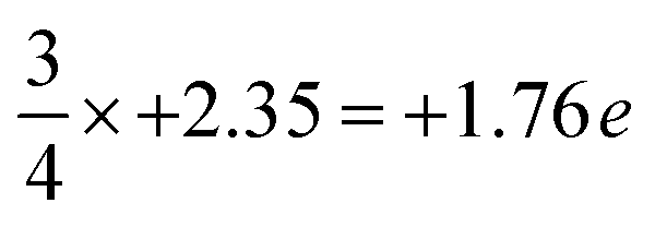 ; as surface N1 atoms have three instead of four bonds). The charge of the corresponding uppermost Al1 atoms (−2.36 e) is nearly the same as the bulk Al atoms in the lower layers of −2.35 e, while the N2 atoms just below Al1 show a slight decrease in the electron gain (+2.27 e) along with a localized p-orbital peak for the pDOS at the Fermi level. This suggests synergistic interactions of N2 with N1 via Al1. Interestingly, the electron density distribution on the surface N1 atoms is uneven, with pockets of positive charge along the axial positions and negative charge residing along the equatorial positions. This has implications for the preference of interfacial stacking sequence of the electrode layer on the N-terminated AlN slab, which will be further elaborated in the subsequent section.
3.2. Elucidating the interface phenomena of different electrodes on AlN slabs
To investigate the electrode layers on AlN slabs, we analyze the formation energy Eif of the electrode layer on the slabs, which determines the stability and polarity preference of AlN. The formation energy can be defined as | (2) |
Considering the three possible interfacial stacking sequences for the electrode layer atoms on Al- and N-terminated AlN slabs (depicted in Fig. 1), we calculate the formation energies for 37 different electrode layers, resulting in a total of 222 interface systems (Fig. 3). It is important to note that in this context, the Al-terminated AlN slab is considered N-polar, in which the N atoms in each AlN bilayers are further away from the electrode layer as compared to the Al atoms in the same bilayer. The reverse holds true for the Al-polar N-terminated AlN slab.
 | ||
| Fig. 3 (a)–(d) Plots of formation energy of the electrode layer–AlN slab interface system Eif with respect to the electrode layer elements i for the three different interfacial stacking sequences (top, hcp, fcc) and two polarities (N- and Al-polarity). (e) Plots of comparison between the average formation energy of the electrode layer–AlN slab interface system with AlN slabs of N- and Al-polarity for the (i) main group elements, (ii) first row transition metals, (iii) second row transition metals, and (iv) third row transition metals, respectively. The dashed lines separate the polarity preference of the electrode layer elements with the upper and lower half of the plots favoring Al- and N-polarity, respectively. (f) Plot of formation energy of the electrode layer–AlN slab interface system Eifversus the distance between the electrode layer and the interface layer of the AlN slab. The linear best fit lines for the different interfacial stacking sequences and two AlN slab polarities are also included as dotted lines with the linear correlation coefficients R2 ranging from 0.84 to 0.97. (g) Plot of formation energy of the electrode layer–AlN slab interface system Eifversus the Bader charge of the electrode layer. A positive or negative value of Bader charge implies the electrode layer to be negatively or positively charged, respectively. The linear best fit lines for the different interfacial stacking sequences and two AlN slab polarities are also included as dotted lines with the linear correlation coefficients R2 ranging from 0.85 to 0.98. | ||
From the formation energies of the electrode layers on AlN slabs with both polarities and three possible interfacial stacking sequences, several observations can be made:
(I) All the formation energies are negative, indicating the thermodynamically favorable interactions between the electrode layer and AlN slabs. This is expected as the interaction resembles surface adsorption, reducing residual forces at the interfaces by eliminating surface dangling bonds of Al- and N-terminated AlN slabs and the electrode surface, thereby stabilizing the system. The plot of the formation energies and the equilibrium interlayer separations between the electrode layer and the interface layer of the AlN slabs are illustrated in Fig. 3(f). It can be observed that the separation distance for electrode layers on N-polar AlN slabs are generally larger than those on Al-polar AlN slabs due to the larger size of the Al interface atoms of N-polar slabs (rAl = 125 pm)37 compared to the N interface atoms of Al-polar ones (rN = 65 pm).37 Moreover, more negative formation energies or higher stability occur with shorter interlayer separations. This is believed to be arising from the stronger electrostatic interfacial interactions which would be discussed in the next paragraph.
(II) There is a clear direct relationship between the formation energies and the Bader charges of the electrode layer (Fig. 3(g)), with larger magnitudes of the Bader charge corresponding to the more negative formation energy. As for electrode layers on Al-polar AlN slabs, they all show a loss of electrons with negative Bader charges. This is due to electron transfer from less electronegative electrode layer atoms to highly electronegative N1 atoms at the electrode layer–AlN interface which also leads to a corresponding increase in the Bader charge for the N1 atoms (Fig. S1, ESI†) and also a reduction in interlayer separation. The electron localization function (ELF)38 contour plots along the (110) plane (Fig. S2, ESI†) show the electrons to be mostly localized or separated from those of the AlN slabs. These suggest the primary form of interface interaction is mostly electrostatic or ionic in nature. The same explanation applies to the electrode layers on N-polar AlN slabs, where electron transfer occurs from Al1 atoms to the electrode layer for more electronegative electrode layer elements.
(III) Comparing the formation energies of the top interfacial stacking sequence with those of the hcp and fcc interfacial stacking sequence (Fig. S3, ESI†), the top interfacial stacking sequence is preferred for most electrode layer elements on Al-polar AlN slabs (hcp and fcc interfacial stacking sequence less stable on average by 53 and 35 meV Å−2, respectively). This preference minimizes potential lattice distortion and destabilization, while ensuring interfacial structural continuation by aligning with the overall wurtzite structure of the AlN slabs. The reduced electron density along the axial position of the N1 atoms of the N-terminated or Al-polar AlN slabs as illustrated in Fig. 2(d), creates an electrostatically favorable location for the electrode layer atoms, favoring the top interfacial stacking sequence. Some of the optimized structures also transformed from the initial hcp (e.g., C, Si, Os, and Ir) or fcc (e.g., C, Os, Ir, and Pt) interfacial stacking sequence to the top interfacial stacking sequence. However, for the N-polar counterpart, no distinct interfacial stacking sequence is observed, and the top interfacial stacking sequence is generally slightly less stable than the hcp and fcc stacking sequences (top interfacial stacking sequence less stable than hcp and fcc on average by 12 and 6 meV Å−2, respectively). The lack of interfacial stacking preference is due to the absence of the reduced electron density along the axial position of the Al1 atoms of the N-polar AlN slab (Fig. 2(b)).
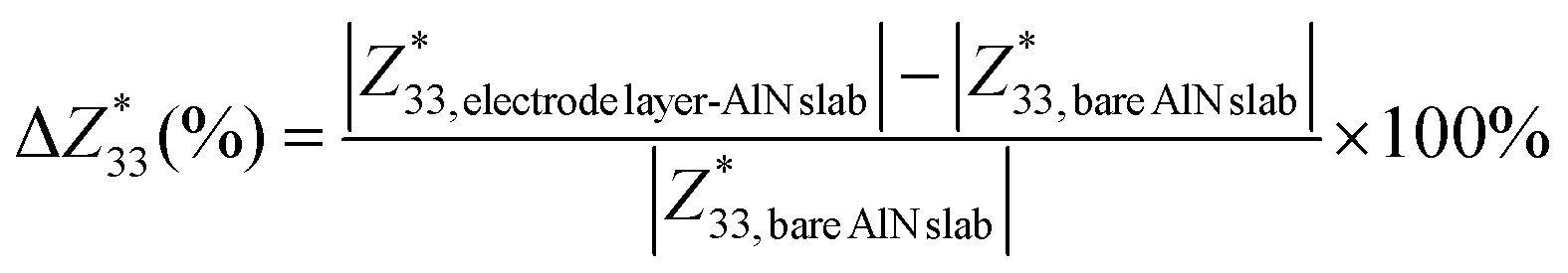
Owing to the pseudo-2D characteristics inherent in the electrode layer–AlN slab interface system, with vacuum effects, finite slab size, and the pseudo-hydrogen capping of the slab, a straightforward comparison of the calculated Born effective charges (BECs) with those of bulk AlN poses inherent complexities. Nonetheless, given the specific focus of our investigation on the electrode layer on the AlN slab, we adopt an alternative methodology. Our approach involves evaluating the ratio of the change in the BEC of the interfacial atom of the AlN slab of the electrode layer–AlN slab interface system to the BEC of the same atom of the bare AlN slab:
 | (3) |
 is the percentage change in the magnitude of BEC of the axial component of the interfacial atom of the AlN slab due to the electrode layer, while
  and
and  correspond respectively to the as-calculated BEC of the axial component of the interfacial atom of the electrode layer–AlN slab and the as-calculated BEC of the axial component of the same atom on the bare AlN slab. Given the direct correlation between the BEC
  and the piezoelectric coefficient (e33), i.e.,
  ,39–42 an increase or decrease in
  would therefore indicate an associated enhancement or reduction of the piezoelectric properties of the AlN slab. From Fig. S4 (ESI†), we can observe that the addition of the electrode layer would generally lead to an increase in
  , suggesting an improved piezoelectric performance of AlN with the electrode layer.
To further understand these observations and polarity preference of AlN with different electrode layers, we introduce the concept of “polar tendency”. The polar tendency is defined as the ratio of the average (among three stacking sequence) formation energy of an electrode layer i on the AlN slab with Al-polarity Ēif,Al-Polar to the average formation energy of the same electrode layer i on the AlN slab with N-polarity Ēif,N-Polar:
 | (4) |
A positive or negative value of the polar tendency indicates a preference of AlN slabs with Al- or N-polarity, respectively, for the electrode layer element i while a value of close to 0 suggests no polarity preference and the experimentally observed polarity would therefore mainly depend on external factors such as synthesis conditions and post-processing.8,11,12 By plotting electronegativity versus polar tendency (Fig. 4(a)), a direct linear relationship is observed, indicating that the less electronegative the electrode layer element, the stronger the tendency towards Al-polarity. This is as rationalized by the electrostatic preference of less electronegative electrode layers for the partially negatively charged N atoms on the N-terminated surface of Al-polar AlN slabs. Notably, the evaluated polar tendency agrees with experimental observations of Al-polarity on Al and Si electrodes,11,43 and N-polarity on Pt and Ru electrodes.10,43 From the plot, we can predict that Au and Sc would be perfect electrodes on AlN slabs with strong N- and Al-polarity preference, respectively. Therefore, electronegativity can be a primary consideration in designing electrode–AlN slab systems with a preferred polarity.
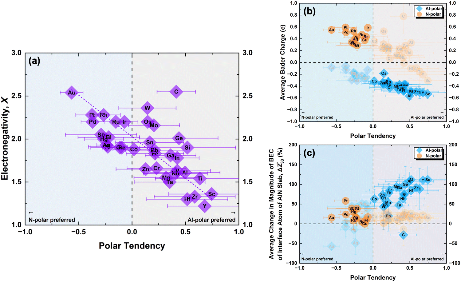 | ||
| Fig. 4 (a) Plot of electronegativity X versus polar tendency for the various electrode layer elements on AlN slab. The black dashed line separates the polarity preference of the electrode layer elements with the left and right half of the plot indicating preference of the AlN slab towards N- and Al-polarity, respectively. The purple dashed line is the linear best fit line with a linear correlation coefficient R2 of 0.85. (b) Plot of average Bader charge versus polar tendency for the various electrode layer elements on the AlN slab. The black vertical dashed line separates the polarity preference of the electrode layer elements with the left and right half of the plot indicating preference of the AlN slab towards N- and Al-polarity, respectively. (c) Plot of average percentage change in the Born effective charge of the interface atoms of the AlN slab for the various electrode–AlN slab systems. The black vertical dashed line separates the polarity preference of the electrode layer elements with the left and right half of the plot indicating preference of AlN slab towards N- and Al-polarity, respectively. | ||
Alternatively, instead of electronegativity, which is an inherent property of an element, the average Bader charge of the electrode layer for each AlN slab polarity and the average change in the BEC of the interface atoms on the AlN slab can be plotted against the polar tendency. Looking at the Bader charges (Fig. 4(b)), electrode layers with Al-polarity tendency exhibit lower Bader charges compared to those with a tendency towards N-polar AlN slabs. Simulation of AlN slabs with oxidized Ru electrodes reveals a reduction of N-polarity preference, accompanied by a decrease in the Bader charge for Ru (Fig. S5, ESI†), consistent with experimental studies10 while beyond the scope of our investigation, this suggests that our approach can potentially predict AlN polarity preference of compound electrodes with two or more element combinations as well. Additionally, examining the BEC (Fig. 4(c)) indicates that the increase in the magnitude of BEC is achievable for almost all electrode layer elements with the preferred AlN polarity. One notable exception is C which could be due to the mainly covalent interaction with the AlN slab (Fig. S2, ESI†). Interestingly, for the electrodes which lead to significant increase in the magnitude of BEC of the interface atom of AlN slab, such as Sc and Y, these elements have also been utilized in doping of AlN for piezoelectric enhancements.44,45 This suggests a potential avenue for optimizing the design of electrode doped-AlN slab systems, opening up new possibilities for advanced materials engineering and device applications.
4. Conclusions
In summary, we have provided a comprehensive analysis of electrode layers on AlN slabs, shedding light on their influence on the stability and polarity preferences of AlN. Through calculations of formation energy and examination of Bader charges, we have established that the interaction between electrode layers and AlN slabs is thermodynamically favorable and is predominantly driven by electrostatic or ionic forces. The preference for the top interfacial stacking sequence on Al-polar AlN slabs aligns with the wurtzite structure, ensuring minimal lattice distortion and interfacial structural continuation. Moreover, the Born effective charge variation of the interfacial atoms on AlN slabs, which depends on the electronegativity of the electrode layer, has a direct impact on interface polarization and the piezoelectric properties. By considering electronegativity or average Bader charges, it becomes possible to design stable electrode on AlN slabs with the desired polarity. We believe that future investigations should explore polarity predictions on compound electrodes with diverse element combinations via doping or alloying, expanding the scope and applicability of our approach. In conclusion, the findings from this analysis of electrode layers on AlN slabs contribute crucial insights for the design and optimization of AlN-based electronic and piezoelectric devices.Conflicts of interest
The authors declare no competing financial interest.Acknowledgements
This work is supported by the Agency for Science, Technology and Research (A*STAR) of Singapore (Grant ID: A20G9b0135). The authors would like to acknowledge the use of the high-performance computing facilities provided by the National Supercomputing Centre Singapore (NSCC) and A*STAR Computational Resource Centre (A*CRC). Z. M. W. would like to dedicate this work in memory of his faithful companion Dotdot Wong.References
- H. P. Loebl, C. Metzmacher, R. F. Milsom, P. Lok, F. van Straten and A. Tuinhout, RF Bulk Acoustic Wave Resonators and Filters, J. Electroceram., 2004, 12(1), 109–118 CrossRef CAS.
- K. Tsubouchi and N. Mikoshiba, Zero-Temperature-Coefficient SAW Devices on AlN Epitaxial Films, IEEE Trans. Sonics Ultrason., 1985, 32(5), 634–644 Search PubMed.
- R. M. R. Pinto, V. Gund, R. A. Dias, K. K. Nagaraja and K. B. Vinayakumar, CMOS-Integrated Aluminum Nitride MEMS: A Review, J. Microelectromech. Syst., 2022, 31(4), 500–523 CAS.
- S. T. Haider, M. A. Shah, D. G. Lee and S. Hur, A Review of the Recent Applications of Aluminum Nitride-based Piezoelectric Devices, IEEE Access, 2023, 1 Search PubMed.
- Y. Iwazaki, T. Yokoyama, T. Nishihara and M. Ueda, Highly enhanced piezoelectric property of co-doped AlN, Appl. Phys. Express, 2015, 8(6), 061501 CrossRef.
- M. Uehara, H. Shigemoto, Y. Fujio, T. Nagase, Y. Aida, K. Umeda and M. Akiyama, Giant increase in piezoelectric coefficient of AlN by Mg-Nb simultaneous addition and multiple chemical states of Nb, Appl. Phys. Lett., 2017, 111(11), 112901 CrossRef.
- S. A. Anggraini, M. Uehara, K. Hirata, H. Yamada and M. Akiyama, Polarity Inversion of Aluminum Nitride Thin Films by using Si and MgSi Dopants, Sci. Rep., 2020, 10(1), 4369 CrossRef PubMed.
- T. Kamohara, M. Akiyama and N. Kuwano, Influence of polar distribution on piezoelectric response of aluminum nitride thin films, Appl. Phys. Lett., 2008, 92(9), 093506 CrossRef.
- A. Iqbal and F. Mohd-Yasin, Reactive Sputtering of Aluminum Nitride (002) Thin Films for Piezoelectric Applications: A Review, Sensors, 2018, 18(6), 1797 CrossRef PubMed.
- J. A. Ruffner, P. G. Clem, B. A. Tuttle, D. Dimos and D. M. Gonzales, Effect of substrate composition on the piezoelectric response of reactively sputtered AlN thin films, Thin Solid Films, 1999, 354(1), 256–261 CrossRef CAS.
- M. Akiyama, T. Kamohara, K. Kano, A. Teshigahara and N. Kawahara, Influence of oxygen concentration in sputtering gas on piezoelectric response of aluminum nitride thin films, Appl. Phys. Lett., 2008, 93(2), 021903 CrossRef.
- T. Kamohara, M. Akiyama, N. Ueno, M. Sakamoto, K. Kano, A. Teshigahara, N. Kawahara and N. Kuwano, Influence of sputtering pressure on polarity distribution of aluminum nitride thin films, Appl. Phys. Lett., 2006, 89(24), 243507 CrossRef.
- G. Schönweger, A. Petraru, M. R. Islam, N. Wolff, B. Haas, A. Hammud, C. Koch, L. Kienle, H. Kohlstedt and S. Fichtner, From Fully Strained to Relaxed: Epitaxial Ferroelectric Al1−xScxN for III-N Technology, Adv. Funct. Mater., 2022, 32(21), 2109632 CrossRef.
- P. C. Sherrell, M. Fronzi, N. A. Shepelin, A. Corletto, D. A. Winkler, M. Ford, J. G. Shapter and A. V. Ellis, A bright future for engineering piezoelectric 2D crystals, Chem. Soc. Rev., 2022, 51(2), 650–671 RSC.
- C. Cui, F. Xue, W.-J. Hu and L.-J. Li, Two-dimensional materials with piezoelectric and ferroelectric functionalities, npj 2D Mater. Appl., 2018, 2(1), 18 CrossRef.
- M. K. Mohanta, F. Is, A. Kishore and A. De Sarkar, Spin-Current Modulation in Hexagonal Buckled ZnTe and CdTe Monolayers for Self-Powered Flexible-Piezo-Spintronic Devices, ACS Appl. Mater. Interfaces, 2021, 13(34), 40872–40879 CrossRef CAS PubMed.
- J. Qiu, X. Chen, F. Zhang, B. Zhu, H. Guo, X. Liu, J. Yu and J. Bao, Highly adjustable piezoelectric properties in two-dimensional LiAlTe2 by strain and stacking, Nanotechnology, 2022, 33(5), 055702 CrossRef CAS PubMed.
- W. Kohn and L. J. Sham, Self-Consistent Equations Including Exchange and Correlation Effects, Phys. Rev., 1965, 140(4A), A1133–A1138, DOI:10.1103/PhysRev.140.A1133.
- J. P. Perdew, K. Burke and M. Ernzerhof, Generalized Gradient Approximation Made Simple, Phys. Rev. Lett., 1996, 77(18), 3865–3868, DOI:10.1103/PhysRevLett.77.3865.
- J. P. Perdew, K. Burke and M. Ernzerhof, Generalized Gradient Approximation Made Simple [Phys. Rev. Lett. 77, 3865 (1996)], Phys. Rev. Lett., 1997, 78(7), 1396, DOI:10.1103/PhysRevLett.78.1396.
- G. Kresse and J. Furthmüller, Efficiency of ab-initio total energy calculations for metals and semiconductors using a plane-wave basis set, Comput. Mater. Sci., 1996, 6(1), 15–50, DOI:10.1016/0927-0256(96)00008-0.
- G. Kresse and J. Furthmüller, Efficient iterative schemes for ab initio total-energy calculations using a plane-wave basis set, Phys. Rev. B: Condens. Matter Mater. Phys., 1996, 54(16), 11169–11186, DOI:10.1103/PhysRevB.54.11169.
- P. E. Blöchl, Projector augmented-wave method, Phys. Rev. B: Condens. Matter Mater. Phys., 1994, 50(24), 17953–17979, DOI:10.1103/PhysRevB.50.17953.
- S. Grimme, J. Antony, S. Ehrlich and H. Krieg, A consistent and accurate ab initio parametrization of density functional dispersion correction (DFT-D) for the 94 elements H-Pu, J. Chem. Phys., 2010, 132(15), 154104 CrossRef.
- H. J. Monkhorst and J. D. Pack, Special points for Brillouin-zone integrations, Phys. Rev. B: Condens. Matter Mater. Phys., 1976, 13(12), 5188–5192, DOI:10.1103/PhysRevB.13.5188.
- H. Schulz and K. H. Thiemann, Crystal structure refinement of AlN and GaN, Solid State Commun., 1977, 23(11), 815–819 CrossRef CAS.
- A. Jain, S. P. Ong, G. Hautier, W. Chen, W. D. Richards, S. Dacek, S. Cholia, D. Gunter, D. Skinner and G. Ceder, et al., Commentary: The Materials Project: A materials genome approach to accelerating materials innovation, APL Mater., 2013, 1(1), 011002 CrossRef.
- J. Kioseoglou, E. Kalesaki, L. Lymperakis, G. P. Dimitrakopulos, P. Komninou and T. Karakostas, Polar AlN/GaN interfaces: Structures and energetics, Phys. Status Solidi A, 2009, 206(8), 1892–1897 CrossRef CAS.
- Razia, M. Chugh and M. Ranganathan, Surface energy and surface stress of polar GaN(0001), Appl. Surf. Sci., 2021, 566, 150627 CrossRef CAS.
- V. Jindal and F. Shahedipour-Sandvik, Density functional theoretical study of surface structure and adatom kinetics for wurtzite AlN, J. Appl. Phys., 2009, 105(8), 084902 CrossRef.
- D. Holec and P. H. Mayrhofer, Surface energies of AlN allotropes from first principles, Scr. Mater., 2012, 67(9), 760–762 CrossRef CAS PubMed.
- G. Henkelman, A. Arnaldsson and H. Jónsson, A fast and robust algorithm for Bader decomposition of charge density, Comput. Mater. Sci., 2006, 36(3), 354–360 CrossRef.
- E. Sanville, S. D. Kenny, R. Smith and G. Henkelman, Improved grid-based algorithm for Bader charge allocation, J. Comput. Chem., 2007, 28(5), 899–908 CrossRef CAS PubMed.
- W. Tang, E. Sanville and G. Henkelman, A grid-based Bader analysis algorithm without lattice bias, J. Phys.: Condens. Matter, 2009, 21(8), 084204, DOI:10.1088/0953-8984/21/8/084204.
- M. Yu and D. R. Trinkle, Accurate and efficient algorithm for Bader charge integration, J. Chem. Phys., 2011, 134(6), 064111 CrossRef PubMed.
- C. M. Fang and Z. Fan, Atomic Ordering at the Interfaces Between Liquid Aluminum and Polar AlN{0 0 0 1} Substrates, Metall. Mater. Trans. A, 2022, 53(6), 2040–2047 CrossRef CAS.
- J. C. Slater, Atomic Radii in Crystals, J. Chem. Phys., 1964, 41(10), 3199–3204 CrossRef CAS.
- B. Silvi and A. Savin, Classification of chemical bonds based on topological analysis of electron localization functions, Nature, 1994, 371(6499), 683–686 CrossRef CAS.
- M. A. Caro, S. Schulz and E. P. O’Reilly, Theory of local electric polarization and its relation to internal strain: Impact on polarization potential and electronic properties of group-III nitrides, Phys. Rev. B: Condens. Matter Mater. Phys., 2013, 88(21), 214103 CrossRef.
- K. Hirata, H. Yamada, M. Uehara, S. A. Anggraini and M. Akiyama, First-Principles Study of Piezoelectric Properties and Bonding Analysis in (Mg, X, Al)N Solid Solutions (X = Nb, Ti, Zr, Hf), ACS Omega, 2019, 4(12), 15081–15086 CrossRef CAS PubMed.
- S. Hong, S. M. Nakhmanson and D. D. Fong, Screening mechanisms at polar oxide heterointerfaces, Rep. Prog. Phys., 2016, 79(7), 076501 CrossRef PubMed.
- Y. Okuno and Y. Sakashita, Born Effective Charges and Piezoelectric Coefficients of BiXO3, Jpn. J. Appl. Phys., 2009, 48(9S1), 09KF04 Search PubMed.
- T. Harumoto, T. Sannomiya, Y. Matsukawa, S. Muraishi, J. Shi, Y. Nakamura, H. Sawada, T. Tanaka, Y. Tanishiro and K. Takayanagi, Controlled polarity of sputter-deposited aluminum nitride on metals observed by aberration corrected scanning transmission electron microscopy, J. Appl. Phys., 2013, 113(8), 084306 CrossRef.
- M. Akiyama, T. Kamohara, K. Kano, A. Teshigahara, Y. Takeuchi and N. Kawahara, Enhancement of Piezoelectric Response in Scandium Aluminum Nitride Alloy Thin Films Prepared by Dual Reactive Cosputtering, Adv. Mater., 2009, 21(5), 593–596 CrossRef CAS PubMed.
- C. Tholander, I. A. Abrikosov, L. Hultman and F. Tasnádi, Volume matching condition to establish the enhanced piezoelectricity in ternary (Sc,Y)0.5(Al,Ga,In)0.5N alloys, Phys. Rev. B: Condens. Matter Mater. Phys., 2013, 87(9), 094107 CrossRef.
Footnote |
| † Electronic supplementary information (ESI) available: Convergence tests for the determination of the number of AlN bilayers for AlN slabs of N- and Al-polarity, the justification for the number of electrode layers implemented, and vacuum density selection for Bader charge analyses; plot of formation energy of the electrode layer–AlN slab interface system for the three different interfacial stacking sequences and two polarities with respect to the change in Bader charge of interface atoms of the AlN slab; plot of the Bader charge of the electrode layer versus the corresponding change in the Bader charge of the interface atom of the AlN slab; contour plots of the electron localization function for the various electrode layer elements on the AlN slab; histogram plots for formation energy difference between hcp and top interfacial stacking sequence of electrode layers on the Al-polar AlN slab, fcc and top interfacial stacking sequence of electrode layers on the Al-polar AlN slab, hcp and top interfacial stacking sequence of electrode layers on the N-polar AlN slab, and the fcc and top interfacial stacking sequence of electrode layers on the N-polar AlN slab; histogram plots for the percentage change in the Born effective charge of the interface atom of the AlN slab for the top, hcp, and fcc interfacial stacking sequence of both polarities; plot of average Bader charge versus polar tendency for the various electrode layer elements on the AlN slab with emphasis on Ru and oxidized Ru species; representative structures of the RuO electrode with N- and Al-polar AlN slabs. See DOI: https://doi.org/10.1039/d3ma00842h |
| This journal is © The Royal Society of Chemistry 2024 |