
 Open Access Article
 This Open Access Article is licensed under a Creative Commons Attribution-Non Commercial 3.0 Unported Licence
Harnessing infrared radiation using carbon dots: photovoltaic devices achieving extraordinary efficiency under faint lighting†
Karan
Surana
 a,
Bhaskar
Bhattacharya
b and
Saurabh S.
Soni
*ac
a,
Bhaskar
Bhattacharya
b and
Saurabh S.
Soni
*ac
aDepartment of Chemistry, Sardar Patel University, Vallabh Vidyanagar 388120, Gujarat, India. E-mail: soni_b21@yahoo.co.in; saurabh_soni@spuvvn.edu
bDepartment of Physics, Mahila Mahavidyalaya, Banaras Hindu University, Varanasi 221005, Uttar Pradesh, India
cDepartment of Applied and Interdisciplinary Sciences, IICISST, Sardar Patel University, Vallabh Vidyanagar 388120, Gujarat, India
First published on 28th November 2023
Abstract
Developing photovoltaic devices capable of functioning under low-light intensities is necessary for developing future-ready technologies. Carbon dots (CD) are one such material that hold potential for a wide variety of practical applications, including low-light responsive photovoltaic cells capable of powering IoT devices. This current work depicts the preparation of CDs via solvothermal and microwave methods and their applications in dye-sensitized solar cells (DSSCs) as a co-sensitizer with the N719 dye. The prepared CDs are able to harness infrared radiation, which is confirmed by multiple measurement techniques. Additionally, a synergistic interaction is noticed between the N719 dye and the CDs, which allowed the device to function under dim light as well as under 1 sun. The device exhibited an extraordinary efficiency of over 80% under faint lighting.
1. Introduction
The processing of natural materials to produce functional green carbon (C) or graphene (G) dots has been greatly increased in recent years. The advantage of using natural precursors for synthesis lies in their abundance, availability, non-toxicity, and renewable nature.1,2 Unlike other carbon allotropes, carbon dots (CD) are colorful dots having a size of a few nanometers only. Their excellent optical and electrochemical properties have paved the way for their application in various areas, such as biomedical imaging and sensing, chemical sensing, drug delivery, photocatalysis and photovoltaic devices.3–9 The solubility of CDs in aqueous media presents an added advantage for their ease of application. Traditional inorganic quantum dots show fluorescent properties owing to their quantum confinement effect; however, in the case of CDs, the surface passivation phenomenon plays a dominant role.6,9Moreover, technology has made tremendous progress in the last decade, enabling mankind to have almost anything at its fingertips. This has led to a surge in the number of smart devices available in a common household, which has consequently led to increased power consumption. This power demand is going to extensively increase in the future. One of the possible solutions to fulfill this energy demand is to have indoor photovoltaic devices, which can run effectively even on low input power, such as certain types of third generation solar cells.10–14 Although these solar cells are a subset of the prevalent photovoltaic devices, research in this direction is still in its early stages. Hou et al. reported a solid-state quantum dot solar cell (QDSC) comprising ZnO QDs and PbS QDs, which showed an efficiency (η) of 19.5% at 2000 lux and 9.55% under 1 sun (active area 0.012 cm2).15 Venkatesan reported the use of N719, MK-2, YD2-o-C8 and Z907 dyes with a quasi-solid polymer electrolyte (PEO/PVDF/TiO2/I) and achieved a η of 20.67% under 600 lux.16 Freitag et al. reported the application of D35 and XY1 organic dye with a Cu complex redox couple, which yielded a η of 28.9% under 1000 lux in ambient white light.17 CDs have been successfully employed in dye/QD/perovskite sensitized solar cells and have given favorable output, especially as co-sensitizers.9,18,19 In a report by Efa et al. dye-sensitized solar cells (DSSC) were fabricated using ZnO nanoparticles embedded with and without CDs and sensitized with the N719 dye. The best performing device with N719 dye-sensitized ZnO resulted in a η of 2.90%, while CD-embedded ZnO sensitized with the N719 dye showed a η of 5.92% at an input power of 156 W m−2.20 Another report by Etefa et al. reported a similar study with NiO and achieved roughly four times enhancement in efficiency. Furthermore, it was also indicated that the enhancement was a result of the synergistic effect caused by the co-adsorption of CD and N719 dye.21 In a recent work by Kalra et al. the synergistic effect of CDs was observed with perylene diimide dye, which led to eleven times enhancement in efficiency in the co-sensitized device.22 It should be noted that the N719 dye alone is not suitable for indoor or low light applications owing to the partial availability of light in its absorption spectrum; hence, it is almost always used with some modification or with a co-sensitizer.23,24
One of the chief advantages of the co-sensitization strategy lies in the better coverage of the available electromagnetic spectrum, thus creating the possibility of greater number of photon-to-exciton conversion. Keeping this in mind, in the current work, we have used collard greens as our precursor for synthesizing carbon dots. Collard greens are green leafy vegetables belonging to the cruciferous family having tremendous health benefits. In India, they are grown mainly in the Kashmir region; however, they are widely available in African and American nations.25,26 By varying the solvents and synthesis process we have been able to prepare CD with blue, green, and red luminescence. Furthermore, the prepared CD were characterized by optical and microscopic methods to assess their properties and size. The red luminescent CD was employed as a co-sensitizer in the solar cell along with the N719 dye, and the performance was evaluated under various light conditions.
2. Experimental
The synthesis of CD from collard green leaves was performed by microwave, hydrothermal, and solvothermal method using acetone, water and ethanol, and dimethylformamide (DMF), respectively, as solvents. The use of different solvents would result in the extraction of different pigments from the leaves. A detailed procedure is given in the ESI† (materials and methods) while the images of the extracts and their corresponding CD along with their luminescence under UV light is shown in Fig. 1. The synthesized CD showed luminescence colors in dark turquoise, camouflage green, and dark burgundy for CG (CD from hydrothermal method), CG-SOV (CD from solvothermal method), and CG-MW (CD from microwave method), respectively. Essentially, the prepared CD partially displayed the three primary colors. | ||
| Fig. 1 A schematic representation of the collard green CD synthesis. CG-WE stands for collard greens extract in water and ethanol solvent, CG-DMF stands for collard greens extract in DMF solvent and CG-ACE stands for collard greens extract in acetone solvent while CG, CG-SOV, and CG-MW are their corresponding CDs prepared by hydrothermal, solvothermal and microwave methods, respectively. DL: daylight; UV: ultra-violet light. | ||
Standard protocol was followed for fabricating the DSSCs.9,27 In a typical process, after cleaning the fluorine-doped tin oxide (FTO) glasses, spin-coating of the buffer or blocking layer and platinum solution was performed at ∼1500 rpm for a minute. The FTO glasses were sintered at 450 °C for thirty minutes, followed by doctor blading the TiO2 paste using two pairs of scotch tapes for thickness control. After sintering the electrodes again at 450 °C for thirty minutes, they were subjected to TiCl4 solution treatment, followed by another stage of sintering. Finally, the TiO2 photoanode was sensitized with CG-MW or N719 dye overnight. After rinsing with acetone, quasi-solid iodine-based polymer electrolyte was spread over the photoanode and sandwiched with the platinum-coated counter electrode.28 Further detailing of the protocol and that of a 5 × 1 mini-module is given in the ESI† (Fig. S1, ESI†). The device prepared with the co-sensitization of CD and the N719 dye was named CS1, the device prepared with the sensitization of only CD was named CS2, and the device prepared with only N719 dye sensitization was named CS3. The prepared 5 × 1 mini-module was also co-sensitized with CD and N719 dye and named CS1.5. The instrumental details used for the various characterizations are also presented in the ESI† (characterization tools).
3. Results and discussion
3.1. Absorption and emission characteristics
The different colored extracts and their corresponding CD obtained from the hydrothermal, solvothermal, and microwave methods clearly suggest a variation in their absorption spectrum. Thus, the UV-Vis absorption analysis of the three CD along with their respective untreated dyes is shown in Fig. 2. The water–ethanol-based dye of collard green (CG-WE) shows two strong peaks at 329 nm and 267 nm with a miniature shoulder peak at 244 nm (Fig. 2a). The corresponding CD (CG) shows a weak π–π* transition peak (arising due to sp2 carbon) at 255 nm and an n–π* transition peak (arising due to the surface states) at 324 nm.29 | ||
| Fig. 2 UV-Vis absorption characteristics of (a) CG-WE and CG, (b) CG-DMF and CG-SOV and (c) CG-ACE and CG-MW. | ||
The DMF-based dye of collard green (CG-DMF) shows the typical absorption nature of chlorophyll (dominated by chlorophyll a) with multiple peaks throughout the visible spectrum.30 The major absorption peaks are marked in Fig. 2b. Owing to the use of DMF, there was only noise beyond 270 nm. It is interesting to note that the absorption of chlorophyll extract is in the UV region also, which is seldom shown in the literature. The solvothermally-treated CD (CG-SOV) retains no signature of the dye and shows its absorption maximum at 272 nm with a minor shoulder peak at 400 nm. On the other hand, the acetone-based dye (CG-ACE) shows similar absorption peaks in the visible region as CG-DMF with an additional shoulder peak at 534 nm, which remained unresolved in CG-DMF. Absorption beyond 300 nm could not be obtained owing to the use of acetone as the solvent. Surprisingly, unlike the other two CDs, CG-MW retained the major absorption peaks of its dye with minor shifting (Fig. 2c). This suggests that the microwave treatment possibly caused a reduction in the molecule size without causing a change in its primary porphyrin structure. Consequently, the reduction in particle size led to a blue shift of the primary absorption maximum (430 nm to 410 nm).
Following the absorption characteristics, the photoluminescence (PL) emission of the dyes and their corresponding CD were studied, which are detailed in the ESI† (PL emission) along with their color coordinates (Fig. S2–S5, ESI†). The PL emission of CG-ACE and CG-MW is shown in Fig. 3a. The primary emission characteristics of chlorophyll (CG-ACE) lies in the higher wavelength region of the visible spectrum at 667 nm with a small shoulder peak at approximately 720 nm.31 In case of CG-MW, the emission peak is rather sharp and appears at 670 nm, shifted by 3 nm from CG-ACE with a similar shoulder peak.32,33 This further confirms that the microwave treatment only truncated the molecule without effecting its porphyrin structure, thus retaining its emission characteristics as well.
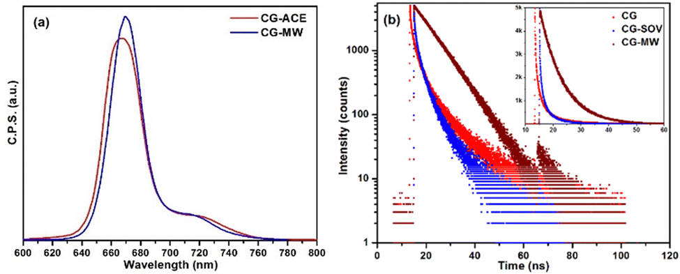 | ||
| Fig. 3 (a) PL emission of CG-ACE and CG-MW at an excitation wavelength of 410 nm. (b) Time-resolved fluorescence decay of the three CDs at an excitation wavelength of 360 nm. | ||
The fluorescence lifetime or electron decay characteristics of the three CD is shown in Fig. 3b. The CDs were excited at a wavelength of 360 nm, and the emission wavelength for CG, CG-SOV, and CG-MW was 430 nm, 430 nm, and 670 nm, respectively. The electron lifetimes of CG, CG-SOV, and CG-MW obtained from bi-exponential fitting were 1.75 ± 0.19 ns, 0.83 ± 0.12 ns, and 7.03 ± 1.54 ns, respectively. The short lifetime generally corresponds to the radiative recombination of the excitons, which is responsible for the occurrence of fluorescence.
3.2. Particle size analysis of CD
The CD prepared with hydrothermal, solvothermal, and microwave methods using the solvents water and ethanol, DMF, and acetone, respectively, showed no visible signs of particle agglomeration under room ambient conditions even after several months of preparation. To gain a visual representation of the particle size distribution, morphology, and crystallinity, the CDs were subjected to high-resolution transmission electron microscopy (HR-TEM). A large field representation of CG is shown in Fig. S6 (ESI†), where ∼200 particles can be seen with a narrow size distribution. The corresponding HRTEM image is shown in Fig. 4a, wherein the dots seem to be well below 5 nm. For a precise size measurement of the formed dots, ImageJ software was used and an estimation was made using fifty particles. The nearly circular-shaped CG particles lied in the range of 1.32 nm to 3.85 nm, and the calculated average particle size was 2.15 ± 0.52 nm. The particles seemed to be well distributed with no sign of agglomeration. | ||
| Fig. 4 HR-TEM images of (a) CG and (inset) SAED pattern, (b) CG-SOV and (inset) the close-up view of a single particle and (c) CG-MW and (inset) the close-up view of a single particle. | ||
The inset of Fig. 4a shows the selective area electron diffraction (SAED) pattern depicting multiple concentric circles. Such occurrence suggests the presence of multiple overlapping crystals in random orientations, resulting in continuous bright spots in the SAED pattern to appear as rings. Therefore, the prepared CD are of a semi-crystalline nature. The calculated d-spacing was obtained to be 0.232 nm.
The TEM images of CD prepared with DMF (CG-SOV) showed better contrast compared to the one prepared with water (CG). The particles also seem to be well-distributed, lying in the size range of 1.57 nm to 4.76 nm with an average particle size of 2.83 ± 0.83 nm (Fig. 4b). The CG-SOV particles also appear to be mostly spherical in shape. The inset of Fig. 4b clearly shows the lattice fringes of a particle, and the calculated d-spacing was found to be 0.241 nm. An HR-TEM image of CG-SOV is shown in Fig. S7 (ESI†). The particles of CG-MW are quite different than the other two. The individual particles are mostly arranged in small colonies of 10–15 each (Fig. 4c). The particles are mostly spherical but are present in other 3-D shapes also. The general size of the QD lies in the range from 1.99 nm to 4.91 nm with an average size of 3.44 ± 0.73 nm. The inset of Fig. 4c shows the close-up view of a particle with clearly visible lattice fringes having a d-spacing of 0.223 nm. Further, the high-resolution image of CG-MW is shown in Fig. S8 (ESI†). Thus, the HR-TEM images show a narrow size distribution of the three CD, thereby confirming the suitability of the employed reaction mechanisms.
The size distribution of the three CD was further analyzed through dynamic light scattering (DLS) measurement, which revealed an average size of lower than 10 nm with few particle sizes up to 100 nm (Fig. 5a). They were later subjected to another round of filtration. The average sizes of the CD are presented in Table 1. The obtained average sizes vary in comparison to that obtained from TEM since all the formed particles are not in a perfect spherical shape.
 | ||
| Fig. 5 (a) DLS measurement and (b) zeta potential of the CD. | ||
| CD | Size distribution (nm) | Zeta potential (mV) |
|---|---|---|
| CG | 3.5 | +86.9 |
| CG-SOV | 9.7 | +98.2 |
| CG-MW | 4.7 | −42.4 |
The zeta potential of the CD was more than ±30 mV, which suggests that the prepared QDs are stable and free from agglomeration (Fig. 5b). However, the zeta potential of only CG-MW holds a net negative charge, signifying the prominence of donor species, while CG and CG-SOV have a net positive zeta potential (excess of acceptor species). Since we require the dominance of n-type species in photovoltaic application, only CG-MW was chosen as the sensitizer. This is also supported by the absorption spectrum (CG-MW shows wider spectrum coverage) and electron lifetime measurements (longer electron lifetime).
3.3. Device measurements
 | ||
Fig. 6 (a) The J–V characteristics and (b) EIS analysis of CS1 under 1 sun (equivalent to 683![[thin space (1/6-em)]](https://www.rsc.org/images/entities/char_2009.gif) 000 lux). The time 0 min denotes the first measurement of the device. 000 lux). The time 0 min denotes the first measurement of the device. | ||
To further understand the above observation, impedance analysis was also undertaken after each I–V measurement (Fig. 6b) under illuminated condition. There was almost no change in RS (series resistance) overtime, which is expected (inset Fig. 6b). A major shift in RC (junction resistance between the photoanode and electrolyte) values toward the lower side can be observed, which perfectly aligns with the increase in the current over time upon light exposure. The reduction in junction resistance suggests that an increment in the number of photogenerated excitons increases over time, thereby resulting in improved Jsc values; however, this needs further investigation. Moreover, it can be observed from Table 2 that the junction capacitance (CC) also improves by almost four times, which could be a contributing factor toward the rise in generated current under continuous irradiation.
 | ||
| Fig. 7 Device exposed to LED lamp at 40 mW cm−2. (a) Impedance analysis at various time intervals; (inset) expanded initial region. (b) Bode plot derived from impedance analysis. | ||
The device characteristics of only CG-MW-sensitized solar cell (CS2) and only N719-sensitized solar cell (CS3) is shown in the ESI† (device characterization, Fig. S9 and S10). Both the devices do not follow the characteristics of CS1. For further assessment, CS1 was kept under low intensity white LED light, radiating a power density of 30 mW cm−2. It can be speculated that owing to the long duration of light exposure, temperature may have a role to play; thus, a temperature sensor probe was also kept in contact with the device. Time-dependent current analysis was performed for 100 min, and the obtained result is shown in Fig. 8a. A sharp rise in current occurred upon turning the lamp ON with an almost linear rise in temperature. The current increased sharply from 1 μA to 50 μA within 100 s while the temperature increased by only 1 °C during this period. Beyond generating 55 μA current, the increment slowed down and the temperature stayed in the range of 33–34 °C. Furthermore, beyond 60 min, the temperature varied by only ±0.5 °C while the current kept rising slowly with no sign of saturation. The observation suggests that temperature may not have a role in the gradual rise in the current of the device, even under low-light intensity.
 | ||
| Fig. 8 I vs. T measurement at (a) 30 mW cm−2 with temperature monitoring for 100 min and (b) 40 mW cm−2 for 300 min. (Inset) J–V characteristics after 300 min of illumination. | ||
To explore the rise in current further, the device was kept in the dark for some time and again subjected to the same LED lamp for measuring the time-dependent current of the device. Even though the device was under constant illumination for 5 h, a similar result was obtained, as shown in Fig. 8b. Comparing Fig. 8a and b, it can be deduced that increasing the light intensity certainly changed the slope of the rising current. It must be noted that room temperature (RT) was kept at 25 °C throughout the measurement; hence, there was negligible fluctuation. Even after 5 h of constant light exposure, no saturation in current was observed, and the current rose to more than twice its initial value. This resulted in a Jsc of 0.40 mA cm−2, a Voc of 0.64 V, and a η of 0.40% after 5 h of light irradiation (inset Fig. 8b). This affirms that the device functions perfectly under low-light conditions and responds in a better way than under 1 sun condition. Since the temperature factor is eliminated, it is speculated that the device might be harvesting the surrounding IR radiation, which causes this unprecedented behaviour.
For the purpose of practical demonstration, a white LED lamp giving an input power of 40 mW cm−2 was used to illuminate four CS1 devices, which were connected in series (generating over 2.3 V shown in movie SV1) and were able to power a digital clock (movie SV2) and a red LED (movie SV3).
 | ||
| Fig. 9 IPCE spectra of the devices. | ||
 | ||
| Fig. 10 Time-dependent analysis of CS1 (a) OCVD with 10 s of light illumination; (b) OCVD under dark condition; (c) current under dark and IR-free condition. | ||
The I vs. T characteristics showed an initial swift decline, followed by multiple slope changes at various time intervals (Fig. 10c). The gradual melting of ice in room ambient condition led to a rise in the temperature from 4 °C to 15 °C, resulting in a slow decline of current. Thus, after approximately 900 s, the device was able to overcome the surrounding IR resilient condition (cold wave), and a distinct rise in current was observed. Since there was no light source shining on the device (directly or indirectly) and the temperature was well below RT, the most plausible source available for the device was the surrounding IR radiation. As the localized temperature slowly reached the room ambient condition, the possibility of available IR radiation increased. Thus, the results obtained till now certainly point toward the involvement of IR energy in the device's power generation. The performance of CS1 under room ambient light of 30 lux is shown in the ESI† (Fig. S11).
At this juncture, it has become imperative to conclusively explore the reason behind the device's unusual performance. Hence, to ascertain the same, four TiO2-coated electrodes were prepared following the usual protocol described earlier. Three of the electrodes were prepared as per the working electrodes of CS1, CS2, and CS3, i.e., TiO2 sensitized with CG-MW and N719 dye, CG-MW, and N719 dye, respectively. The electrodes were subjected to UV-Vis absorption in the range of 400–1100 nm, and their response was recorded (Fig. 11a). The electrode sensitized with CG-MW showed the maximum absorbance in the range of 600–1100 nm amongst all the electrodes, thereby absorbing lower energy radiation in the visible region along with part of the near-IR (NIR) radiation. Its absorption was not amplified in the visible region; hence, it supports the poor I–V characteristics of CS2 (as shown in Fig. S9, ESI†).
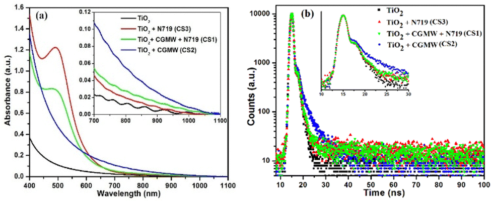 | ||
| Fig. 11 Working electrodes of CS1, CS2 and CS3 along with a TiO2 reference electrode for (a) UV-vis absorption and (b) electron lifetime analysis; (inset) expanded x-axis scale. | ||
The N719-sensitized electrode, as expected, showed comparatively weak characteristics in the NIR region but absorbed greatly in the visible region. On the other hand, the co-sensitized electrode showed relatively enhanced absorbance in the NIR region with slightly reduced characteristics in the visible region in comparison to the only N719 dye-sensitized electrode. Essentially, sensitization with CG-MW aids in absorbing the NIR radiation while the N719 dye absorbs the visible radiation effectively. In an earlier report by Watson et al., it was established that FTO absorbs near-IR (NIR) radiation owing to its large-scale availability of free carriers. This property of FTO aided in the rapid processing of TiO2 and perovskite layer.37,38 Hence, the oscillating absorption nature of the electrodes in the NIR region would also be attributed to the FTO-coated glass. Moreover, as per the UV-Vis absorption, apart from FTO, only CG-MW harvests the NIR radiation. Hence, it is possible that the NIR radiation absorbed by FTO are in turn transmitted to CG-MW.
This effectively confirms the continuously increasing generation of current by CS1 even under dim light or room ambient condition. The observations can be correlated with the rise in CC over time (Table 2). For instance, it is known that various kinds of trap states exist in zero-dimensional quantum dots owing to their small size and discrete energy levels.39,40 It is expected that the NIR radiation are absorbed or trapped in these deep and shallow states, which account for the increasing value of CC with time. Once these accumulated NIR radiation generate enough energy, as per the required energy gap, electron–hole pairs are created, thereby generating current. This phenomenon triggers a series of NIR photons to exciton generation cycle, which may or may not show any signs of attaining saturation, thus resulting in an ever-rising current. Moreover, the UV-Vis observations also suggest that a synergistic interaction could occur between the N719 dye and CG-MW, thereby allowing the device to generate power even under dim light conditions.
The synergistic interaction was confirmed through the electron lifetime measurement wherein the electrodes prepared for UV-Vis measurement were scrapped off from the glass surface and dispersed in equal volume of ethanol. The PL decay/electron lifetimes were measured at an emission wavelength of 650 nm. The obtained electron lifetimes of the working electrodes of CS1, CS2, and CS3 were 2.01 ns, 3.71 ns, and 1.86 ns, respectively. As observed from Fig. 11b, the electron lifetime of CS2 is the highest, which correlates with the UV-Vis observation. On the other hand, the electron lifetime of CS3 is the lowest, which is enhanced in CS1, i.e. upon the presence of N719. This shows that the CD and dye are working in synergy, thus aiding in better power generation and overall device performance.
 | ||
| Fig. 12 Time-dependent current analysis of CS1 performed under IR lamp. | ||
This conclusively shows that the device is capable of harvesting IR energy for generating power, and the constant rise in the current of the device was influenced by the IR absorbing capability of CG-MW. The influence of IR radiation on CS2 is also shown in the ESI† (Fig. S12).
 | ||
| Fig. 13 (a)–(c) Current measurement of the CS1.5 mini-module under sunlight on different days. | ||
Furthermore, measurements were also performed on a day with limited clouds and almost constant sunlight intensity (90–100 mW cm−2) for a considerable duration. This led to a perfect assessment of the device behaviour, as shown in Fig. 13c. In a period of one hour, the generated current increased gradually from few microamperes to over 1.2 mA. Therefore, the performance of CS1.5 under sunlight effectively supplements the two major observations; there is a synergistic interaction between the N719 dye and the prepared CD, and the device is capable of harvesting the surrounding NIR radiation. Both aspects enable the device to perform under room ambient as well as outdoor conditions efficiently.
Finally, the performance of CS1 and CS1.5 was measured under room ambient conditions, and their corresponding J–V characteristics are depicted in Fig. 14. Both the devices showed decent photovoltaic characteristics with CS1.5 generating greater current (almost five times) than CS1 owing to larger area. The equivalent value of 1 lux in W cm−2 is 1.46413 × 10−7.41 Thus, the obtained PCE of CS1 and CS1.5 at 50 lux (7.32 × 10−6 W cm−2) and 100 lux (14.64 × 10−6 W cm−2) is 80.3% and 229.5%, respectively, which is unprecedently high as the formula considers only visible light intensity and there is no provision for inclusion of IR radiation. Moreover, even if the dark current generated by both the devices is eliminated from the Jsc values (measured by keeping the devices in controlled environment overnight), the resultant PCE of CS1 and CS1.5 will be 58.5% and 194.5%, respectively. However, if a factor could be included in the formula to eliminate the IR factor, the actual current conversion through the low-intensity visible light could be calculated.
 | ||
| Fig. 14 J–V characteristics of CS1 and CS1.5 device under faint illumination. | ||
Owing to the growing number of indoor photovoltaics employing various kind of light sources, the concerns of determining reliable conversion efficiency and standardization of testing protocols were raised in a review authored by Hagfeldt et al.42 Keeping the extraordinarily high efficiency aside, the devices are able to generate exceptional current under dark condition, which could be applied for practical application by scaling up the available photon capturing area. Furthermore, it should be noted that the reports available on near-IR light utilizing materials/devices deal with up-conversion or down-conversion phenomenon43–45 while others have reported the synthesis of specifically IR-absorbing dyes for DSSC.46–48 The CD utilized in this work fall in neither category as they directly utilize the IR radiation available in the surroundings and those absorbed by FTO for current conversion.
4. Conclusions
The possibilities of developing a photovoltaic device capable of harnessing low energy radiation such as IR energy and room ambient light should be explored rigorously. Such devices retain the advantage of fast commercialization and large-scale usage. Materials that can show synergistic interaction should be preferred in order to obtain better spectrum coverage and device performance. In the current work, we have been able to synthesize blue, green, and red emissive CD from a green precursor, collard green. All the CD were below 5 nm in size, with the red emissive CD having a net negative zeta potential, which asserted their application in DSSC. The employed combination of red emissive CD and N719 dye showed promising photovoltaic characteristics by generating current in a wide range of conditions. The co-sensitized device performed better than the devices sensitized with only CD or only N719 dye. The efficiency of the device improved from 0.05% to 0.37% with continuous light illumination. Owing to the gradual rise in the generated current, the mini-module was able to deliver over 1.2 mA current under natural sunlight. Moreover, a series combination of four such devices was able to power a red LED and a digital clock under low intensity white light LED (40 mW cm−2). It was concluded that the CD and N719 dye were functioning in synergy while the CD was also able to harvest surrounding IR radiation, thus allowing the device to function even under faint lighting. Owing to the power generation through IR radiation harvesting, the conventional formula used for calculating the efficiency is ineffective and an IR compensating factor should be introduced. In the absence of such a factor, the co-sensitized device CS1 showed an efficiency of 58.52% under 50 lux illumination while the mini-module CS1.5 showed 194.53% efficiency. Owing to its low energy, as of now, the IR radiation can only assist in enhancing the generated current and cannot become the primary source. However, using the CD with another type of IR-responsive dye or quantum dot or increasing the device area could aid in generating enough power to operate IoT devices.Author contributions
Karan Surana: conceptualization, methodology, formal analysis, software, investigation, data curation, writing – original draft, visualization; Bhaskar Bhattacharya: formal analysis, visualization, validation; Saurabh S. Soni: conceptualization, formal analysis, validation, writing – review & editing, visualization, supervision, project administration.Conflicts of interest
There are no conflicts to declare.Acknowledgements
The author KS is grateful to UGC, India for providing the UGC-DS Kothari Postdoc fellowship (No. F. 4-2/2006 (BSR)/CH/20-21/0247). BB gratefully acknowledges the financial assistance as Incentive to Senior Faculties under the Institute of Eminence Scheme (Dev. Scheme No. 6031) from Banaras Hindu University The authors are thankful to SAIF, IIT Bombay and DST-PURSE facility at IICISST, Sardar Patel University for the various characterization facilities. We thank UGC, New Delhi for the central fluorescence measurement facility sponsored under UGC-CAS (Phase-I) program grant vide sanction letter no. F. 540/3/CAS/2011(SAP-I) dated 5th Nov 2011.References
- A. Dager, T. Uchida, T. Maekawa and M. Tachibana, Sci. Rep., 2019, 9(1), 14004 CrossRef PubMed.
- S. Tajik, Z. Dourandish, K. Zhang, H. Beitollahi, Q. Van Le, H. W. Jang and M. Shokouhimehr, RSC Adv., 2020, 10(26), 15406 RSC.
- R. Mohammadi, H. Naderi-Manesh, L. Farzin, Z. Vaezi, N. Ayarri, L. Samandari and M. Shamsipur, J. Pharm. Biomed. Anal., 2022, 114628 CrossRef CAS PubMed.
- R. Mahle, P. Kumbhakar, D. Nayar, T. N. Narayanan, K. K. Sadasivuni, C. S. Tiwary and R. Banerjee, Dalton Trans., 2021, 50(40), 14062 RSC.
- Q. Wang, X. Huang, Y. Long, X. Wang, H. Zhang, R. Zhu, L. Liang, P. Teng and H. Zheng, Carbon, 2013, 59, 192 CrossRef CAS.
- M. Han, S. Zhu, S. Lu, Y. Song, T. Feng, S. Tao, J. Liu and B. Yang, Nano Today, 2018, 19, 201 CrossRef CAS.
- H. Wang, P. Sun, S. Cong, J. Wu, L. Gao, Y. Wang, X. Dai, Q. Yi and G. Zou, Nanoscale Res. Lett., 2016, 11, 1 CrossRef CAS PubMed.
- B. Mistry, H. K. Machhi, R. S. Vithalani, D. S. Patel, C. K. Modi, M. Prajapati, K. R. Surati, S. S. Soni, P. K. Jha and S. R. Kane, Sustainable Energy Fuels, 2019, 3(11), 3182 RSC.
- K. Surana, R. M. Mehra, S. S. Soni and B. Bhattacharya, RSC Adv., 2022, 12(3), 1352 RSC.
- H. S. Ryu, S. Y. Park, T. H. Lee, J. Y. Kim and H. Y. Woo, Nanoscale, 2020, 12, 5792 RSC.
- X. Hou, Y. Wang, H. K. H. Lee, R. Datt, N. U. Miano, D. Yan, M. Li, F. Zhu, B. Hou, W. C. Tsoi and Z. Li, J. Mater. Chem. A, 2020, 8(41), 21503 RSC.
- J. V. Vaghasiya, K. K. Sonigara, L. Suresh, M. Panahandeh-Fard, S. S. Soni and S. C. Tan, Nano Energy, 2020, 60, 457 CrossRef.
- K. K. Sonigara, H. K. Machhi, J. V. Vaghasiya, A. Gibaud, S. C. Tan and S. S. Soni, Small, 2018, 14(36), 1800842 CrossRef PubMed.
- J. Prasad, H. K. Machhi, K. K. Sonigara, V. K. Patel and S. S. Soni, ACS Appl. Mater. Interfaces, 2020, 12(20), 22939 CrossRef CAS PubMed.
- B. Hou, B. S. Kim, H. K. H. Lee, Y. Cho, P. Giraud, M. Liu, J. Zhang, M. L. Davies, J. R. Durrant, W. C. Tsoi and Z. Li, Adv. Funct. Mater., 2020, 30(39), 2004563 CrossRef CAS.
- S. Venkatesan, I. P. Liu, W. N. Hung, H. Teng and Y. L. Lee, Chem. Eng. J., 2019, 367, 17 CrossRef CAS.
- M. Freitag, J. Teuscher, Y. Saygili, X. Zhang, F. Giordano, P. Liska, J. Hua, S. M. Zakeeruddin, J. E. Moser, M. Grätzel and A. Hagfeldt, Nat. Photonics, 2017, 11(6), 372 CrossRef CAS.
- H. Li, W. Shi, W. Huang, E. P. Yao, J. Han, Z. Chen, S. Liu, Y. Shen, M. Wang and Y. Yang, Nano Lett., 2017, 17(4), 2328 CrossRef CAS PubMed.
- K. P. Shejale, A. Jaiswal, A. Kumar, S. Saxena and S. Shukla, Carbon, 2021, 183, 169 CrossRef CAS.
- M. T. Efa and T. Imae, Electrochim. Acta, 2019, 303, 204 CrossRef CAS.
- H. F. Etefa, T. Imae and M. Yanagida, ACS Appl. Mater. Interfaces, 2020, 12(16), 18596 CrossRef CAS PubMed.
- P. Kalra, K. Surana, B. Bhattacharya, G. Singh and G. Durga, J. Mol. Struct., 2023, 1285, 135470 CrossRef CAS.
- M. C. Sil, L. S. Chen, C. W. Lai, Y. H. Lee, C. C. Chang and C. M. Chen, J. Power Sources, 2020, 479, 229095 CrossRef.
- R. Y. Huang, W. H. Tsai, J. J. Wen, Y. J. Chang and T. J. Chow, J. Power Sources, 2020, 458, 228063 CrossRef CAS.
- R. Akhter, F. A. Masoodi, T. A. Wani, J. Raja and S. A. Rather, Ethnic Fermented Foods and Beverages of India: Science History and Culture, 2020, p. 231 Search PubMed.
- L. Z. Lin and J. M. Harnly, J. Agric. Food Chem., 2009, 57(16), 7401 CrossRef CAS PubMed.
- J. V. Vaghasiya, K. K. Sonigara, J. Prasad, T. Beuvier, A. Gibaud and S. S. Soni, J. Mater. Chem. A, 2017, 5(11), 5373 RSC.
- P. K. Singh, R. K. Nagarale, S. P. Pandey, H. W. Rhee and B. Bhattacharya, Adv. Nat. Sci.: Nanosci. Nanotechnol., 2011, 2(2), 023002 Search PubMed.
- X. T. Zheng, A. Ananthanarayanan, K. Q. Luo and P. Chen, Small, 2015, 11(14), 1620 CrossRef CAS PubMed.
- T. Israsena Na Ayudhya, F. T. Posey, J. C. Tyus and N. N. Dingra, J. Chem. Educ., 2015, 92(5), 920 CrossRef CAS.
- R. Pedrós, I. Moya, Y. Goulas and S. Jacquemoud, Photochem. Photobiol. Sci., 2008, 7, 498 CrossRef PubMed.
- F. Qin, J. Bai, Y. Zhu, P. He, X. Wang, S. Wu, X. Yu and L. Ren, Phys. Chem. Chem. Phys., 2023, 25, 2762 RSC.
- W. Li, S. Wu, H. Zhang, X. Zhang, J. Zhuang, C. Hu, Y. Liu, B. Lei, L. Ma and X. Wang, Adv. Funct. Mater., 2018, 28(44), 1804004 CrossRef.
- K. Surana, N. A. Jadhav, P. K. Singh and B. Bhattacharya, Appl. Nanosci., 2018, 8, 2065 CrossRef CAS.
- L. P. Teo, T. S. Tiong, M. H. Buraidah and A. K. Arof, Opt. Mater., 2018, 85, 531 CrossRef CAS.
- N. Prajapati, C. N. Murthy, H. K. Machhi and S. S. Soni, J. Mater. Sci.: Mater. Electron., 2023, 34(32), 2129 CrossRef CAS.
- K. Hooper, M. Carnie, C. Charbonneau and T. Watson, Int. J. Photoenergy, 2014, 2014 Search PubMed.
- J. Troughton, C. Charbonneau, M. J. Carnie, M. L. Davies, D. A. Worsley and T. M. Watson, J. Mater. Chem. A, 2015, 3, 9123 RSC.
- M. Abdellah, K. J. Karki, N. Lenngren, K. Zheng, T. Pascher, A. Yartsev and T. Pullerits, J. Phys. Chem. C, 2014, 118, 21682 CrossRef CAS.
- W. Kwon, J. Lim, J. Lee, T. Park and S. W. Rhee, J. Mater. Chem. C, 2013, 1, 2002 RSC.
- https://hextobinary.com/unit/illuminance/from/lux/to/wpcm2il (Accessed on January 24, 2023).
- M. Kokkonen, P. Talebi, J. Zhou, S. A. Asgari, S. A. Soomro, F. Elsehrawy, J. Halme, S. Ahmad, A. Hagfeldt and S. G. Hashmi, J. Mater. Chem. A, 2021, 9, 10527 RSC.
- S. Hao, Y. Shang, D. Li, H. Ågren, C. Yang and G. Chen, Nanoscale, 2017, 9, 6711 RSC.
- C. Yuan, G. Chen, L. Li, J. A. Damasco, Z. Ning, H. Xing, T. Zhang, L. Sun, H. Zeng, A. N. Cartwright and P. N. Prasad, ACS Appl. Mater. Interfaces, 2014, 6, 18018 CrossRef CAS PubMed.
- D. Li, H. Ågren and G. Chen, Dalton Trans., 2018, 47, 8526 RSC.
- T. Maeda, Y. Hamamura, K. Miyanaga, N. Shima, S. Yagi and H. Nakazumi, Org. Lett., 2011, 13, 5994 CrossRef CAS PubMed.
- A. K. Sarker, M. G. Kang and J. D. Hong, Dyes Pigm., 2012, 92, 1160 CrossRef CAS.
- J. Zhang, H. Shen, W. Guo, S. Wang, C. Zhu, F. Xue, J. Hou, H. Su and Z. Yuan, J. Power Sources, 2013, 226, 47 CrossRef CAS.
Footnote |
| † Electronic supplementary information (ESI) available: Materials and methods, characterization tools, PL emission, device characterization, Fig. S1–S12, Table T1 and videos SV1–SV3. See DOI: https://doi.org/10.1039/d3ma00649b |
| This journal is © The Royal Society of Chemistry 2024 |