
 Open Access Article
 This Open Access Article is licensed under a Creative Commons Attribution-Non Commercial 3.0 Unported Licence
Heterointerfacial adhesion failure mechanism of ultrahigh filler loading containing epoxy composite films for chip substrates†
Shanjun
Ding
 *,
Xiaomeng
Wu
,
Xu
Zhang
,
Mengqi
Gui
,
Zhidan
Fang
* and
Qidong
Wang
*
*,
Xiaomeng
Wu
,
Xu
Zhang
,
Mengqi
Gui
,
Zhidan
Fang
* and
Qidong
Wang
*
Institute of Microelectronics of Chinese Academy of Sciences, Beijing 100029, China. E-mail: shanjunding@gmail.com; fangzhidan@ime.ac.cn; wangqidong@ime.ac.cn
First published on 6th June 2024
Abstract
High adhesion force of chip substrates is crucial for improving chip reliability in the field of microelectronics. However, the flip chip ball grid array (FCBGA) substrate has faced a huge challenge in that the adhesion mechanism of epoxy composite film/copper is not clear so far. Herein, epoxy resin composite film, copper and core board are used to fabricate FCBGA substrates by the lamination method, and then two kinds of FCBGA substrates were obtained based on epoxy–cyanate ester/silica composite and epoxy–phenolic/silica composite films. Their adhesion behavior and mechanism were analyzed by scanning electron microscopy (SEM), X-ray photoelectron spectroscopy (XPS), contact angle measurement and interference microscopy. It is demonstrated that compared with the epoxy–phenolic/silica composite, the ultrahigh filler loading containing epoxy–cyanate ester/silica composite film has a lower adhesion strength, which is mainly attributed to weak mechanical anchoring, low work of adhesion and low bonding force in chemistry as well as high copper oxides at the heterointerfacial areas. This work will provide a guidance in theory and experiment to enhance the interfacial adhesion force of epoxy resin composite films for advanced chip substrates in the future.
Introduction
With the development of emerging technologies such as artificial intelligence (AI), 5G, gig data, high-performance computing (HPC), intelligent automobiles, and data centers, as well as the tremendous demand for high-speed, high-performance, high-bandwidth, low-latency, low-power, multifunctional, and system-level integrated central processing unit (CPU), graphics processing units (GPU), field programmable gate array (FPGA), and other high-end digital chips, chip substrates are gradually evolving towards high computing power, large sizes, high stack layer, fine line, and high frequency.1–5 To carry out multifunctional and intelligent applications, dielectric polymer materials are widely used to prepare chip substrates with high stack layer structure that can realize electrical interconnection, physical protection, support, heat dissipation, and assembly functions.6 However, as chip substrates move towards high stack layer, fine line, high-speed transmission, and low warpage, the line width and spacing on the substrate are reduced to below 5 μm, which will bring a serious challenge to improve interface adhesion between the copper and resin substrate because insufficient adhesion can lead to various issues, making it impossible to complete the fabrication of multi-layer substrates with fine lines.7–9 Therefore, high adhesion force of the chip substrate with large size is extremely desired so far.Organic resin substrate materials used for chip substrates include bismaleimide triazine (BT) resin,10 prepreg (PP),11 resin-coated copper foil (RCC),12 photosensitive insulation materials,13 and Ajinomoto build-up film (ABF).14 However, bismaleimide triazine (BT) resin, prepreg (PP), resin-coated copper foil (RCC) and photosensitive insulation materials all are not suited for fabricating chip substrates with large size because they have a high coefficient of thermal expansion (CTE) and poor process compatibility, as well as low ability of fabricating blind vias. Ajinomoto build-up film (ABF) is an epoxy resin composite film composed of epoxy resin and a large number of different-sized silica particles. It is widely used as a dielectric insulation material in the manufacturing of advanced flip-chip substrates, thanks to its low dielectric performance, low CTE, low processing temperature, high Young's modulus, and strong process ability and process compatibility. Although ABF can satisfy the requirement of fabricating advanced chip substrates due to its nature in physics and chemistry, the interfacial bonding force between copper and ABF for chip substrates with large size, high stack layer and fine line has been a huge challenge so far in the field of chip packaging.
Efforts have been done to enhance the heterointerfacial bonding force of ABF-based chip substrates. For instance, the degree of curing15,16 and surface roughness17–20 of ABF were tuned by controlling curing temperature and curing time as well as etching potion21–23 to improve the interface bonding force, but the increase of bonding force is very limited. Besides, the excessive surface roughness of ABF is harmful for fabricating chip substrates with large size. The plasmas of different elements can obviously enhance the interface bonding force, but this way is quite difficult for the large-scale manufacturing of chip substrates.24–28 Besides, organic group modified silica particles29,30 and metal seed layers (Ni and Ti elements and stainless steel)31–37 were deposited on the surface of ABFs, which are ways to also enhance the interfacial bonding force. However, these modified silica particles and metal seed layers can cause some new problems. For instance, the preparation and uniform dispersion of modified silica particles are difficult to control, while the metal seed layers are difficult to remove during the etching process. In addition, a large number of silica particles and different curing mechanisms were also introduced to ABF,38–40 this situation is helpful to decrease the dielectric performance and coefficient of thermal expansion (CTE), but not conducive to interface bonding force. Based on the above statement, obtaining high interfacial bonding force for realizing chip substrates with large size, high stack layer and high density still faces a huge challenge. In order to find a way to improve adhesion, the interfacial adhesion mechanism of ABF with high filler loading, low polar and CTE needs to be deeply studied.
In this work, we prepared two ABF-based chip substrates by the wet chemistry method to study the adhesion behavior. The surface morphology, surface roughness, mechanical property, adhesion work and interfacial chemical state of samples were tested by scanning electron microscopy (SEM), X-ray photoelectron spectroscopy (XPS) and contact angle measurement to analyze the peel behavior and adhesion mechanism. To our knowledge, such a study has been not reported so far. This study will provide a new guidance in obtaining polymer build-up films with enhanced interfacial adhesion performance by elaborate process controls in the future.
Experimental
Materials
Epoxy–cyanate ester/silica and epoxy–phenolic/silica composites were named as GZ and GX film, respectively. They are supplied by Ajinomoto Fine-Techno Co., Inc., with applications in the microelectronics industry. These materials are received in the form of b-stage films. To prevent unwanted reactions before processing, the composites are stored at −18 °C. The amount of fillers of GX and GZ films is found to be 42 wt% and 66 wt% from product information. The spherical fillers are polydisperse, ranging from 10 to 1200 nm diameter.Curing reaction of epoxy resin composite films
The curing reaction mechanism of epoxy–cyanate ester/silica and epoxy–phenolic/silica composites was reported, according to our previous study.6 And the whole chemical reaction process and mechanism is shown in Fig. S1.†Fabrication of chip substrate and copper/epoxy resin composite films
GX and GZ films with a low degree of curing were first hot-pressed to the surface of the commercial clad laminate (CCL) at 0.8 MPa and 120 °C for 30 seconds under vacuum conditions with a vacuum degree of about −0.1 MPa, and then were heated by two processes to enhance the pre-curing degree of the film at 100 °C for 30 min and 180 °C for 30 min and form the substrate. Subsequently, the ABF surface was desmeared by using swelling and an oxidizer; the detailed experimental process conditions: swelling at 70 °C for 5 min, oxidation at 80 °C for 5 min in potassium permanganate solution, neutralization and cleaning at 70 °C for 5 min and 10 min, respectively. Then, the surfaces of the films were chemically cleaned during pretreatments. The subsequent activation stage consisted of a pre-dip step, an activation step (palladium ions), and then reduction to metallic palladium. The adsorbed palladium clusters act as a heterogeneous catalyst for electroless copper deposition. After electroless plating, the coupons were annealed for copper recrystallization at 190 °C for 1 h. Then, the galvanic copper layer was electroplated on the electroless copper seed layer. Finally, the galvanic copper was recrystallized at 190 °C for 1 h, by that means also achieving the final curing of the ABF layers (post-curing). The whole fabrication processes of chip substrates and copper/epoxy composite films are shown in Fig. 1.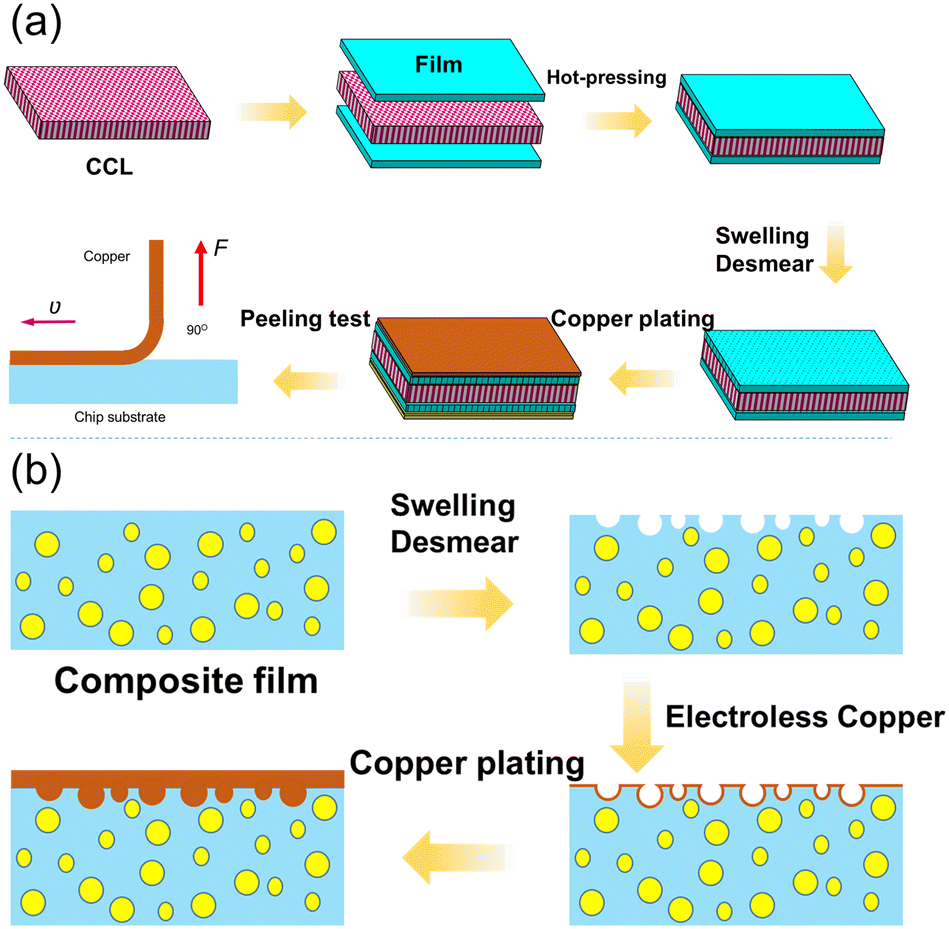 | ||
| Fig. 1 Schematic diagram of (a) the whole fabrication process of chip substrates and (b) preparation processes of copper/epoxy composite films. | ||
Characterization
The cross-section images of polymer composites are examined using a scanning electron microscope (SEM, FEI Nova Nano SEM 450). Optical images of samples are obtained by a polarizing optical microscope (Zeiss Axioskop). Mechanical peel experiments are tested on a RGM-4100 at room temperature with a crosshead speed of 50 mm min−1. Surface roughness of the sample is evaluated using an interference microscope MIC-250 (ATOS GmbH). X-ray photoelectron spectroscopy (XPS) analysis is performed using an XSAM800 (Thermo escalab 250XI, USA), X-ray source: monochromatized Al Kα (1486.6 eV), power: 150 W, beam current: 1.6A, the size of the analyzed area is 650 nm, and the vacuum degree of the analysis room is about 5 × 10⁻⁹ mbar. The contact angles are measured by Dataphysics OCA 20 (Powereach) at room temperature.Results and discussion
Chip substrates are first cut into a small strip, and then this strip is sealed in epoxy resin for easy observation and dissection, as shown in Fig. 2a. After dissection, the microstructure of copper plated ABF is observed on the optical microscope, as shown in Fig. 2b. It was found that the sample is a sandwich structure that consists of the copper layer, ABF and commercial clad laminate (CCL). The surface of the commercial clad laminate (CCL) is deposited with ABF, and the surface of ABF is deposited with the copper layer.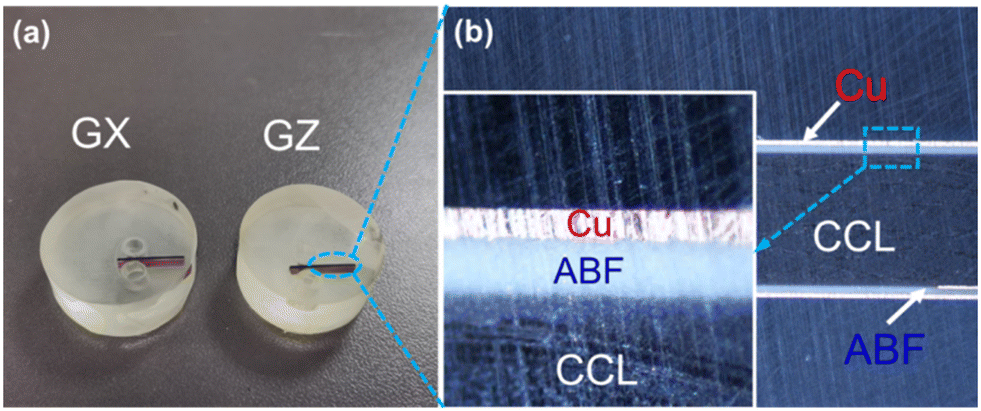 | ||
| Fig. 2 (a) Samples sealed in epoxy resin; (b) the microstructure of chip substrates. | ||
To compare the interfacial adhesion strength of two copper plated films, their peel properties are tested by the tensile peeling test. First, the sample was cut into strips with 10 mm × 50 mm, and then the peel properties of GZ and GX copper plated films are shown in Fig. 3. It can be seen that the peel forces of GZ and GX films are about 3 N and 4 N, respectively. That is, the peel force of the GZ film is obviously lower than that of GX. The results are mainly attributed to the following four aspects: one is that the surface roughness of the GX film is higher than that of the GZ film; two is that there are more additional anchoring points lying in gaps between the silica particle and epoxy resin for the GX film; three is that the content of impurity phases (CuO and Cu2O) for the GZ sample at interface areas is higher than that of the GX sample, and these impurity phases will play a dominant role in the weak boundary layer that can decrease the adhesion property; four is that the work of adhesion of hetero-interfaces between the copper and GX film is obviously higher than that of hetero-interfaces between the copper and GZ film.
 | ||
| Fig. 3 Heterointerfacial adhesion behaviors of the two chip substrates. | ||
Fig. S4 and S5† show the microstructure SEM images of the GX and GZ films from swelling to desmearing processes. The surfaces of the film and copper are observed by SEM when the copper film is peeled off from the film surface. Fig. 4a shows the surface morphology of the GX film. As can be seen, the surface of GX was desmeared uniformly, and at the same time most of the volume of each silica particle is embedded inside the epoxy resin. In addition, by comparing we can see that the roughness of the film surface is higher than that in Fig. S3c,† which indicates that part of the epoxy resin was adhesive onto the surface of copper as well as and silica particles fall off from the ABF surface. Fig. 4b shows the surface morphology of copper plating after being peeled from the film. It was found that there is a high roughness in the copper surface, and we can also observe the formation profiles of many fillers and dents from the coarsening effect on the surface of copper. It is worth noting that this profile of the copper wrapped filler (see yellow areas) indicates that copper atoms enter into gaps between copper and epoxy resin, which will be helpful to form mechanical anchoring and promote the enhancement of adhesion strength. For the GZ film plated copper, the surface morphology of the GZ film and copper layer was observed. Fig. 4c shows the surface morphology of the GZ film. As can be seen, the flat areas on the surface of the GZ film completely disappear in comparison to that in Fig. S4c,† and at the same time most of the volume of each silica particle is embedded inside the epoxy resin. In addition, by comparing we can see that the roughness of the film surface is higher than that in Fig. S4c,† which indicates that part of the epoxy resin was adhesive onto the surface of copper as well as and silica particles fall off from the film surface. Fig. 4d shows the surface morphology of copper plating after being peeled from the film. It was found that there is a high roughness in the copper surface, and we can also observe the formation profiles of many fillers and dents from the coarsening effect on the surface of copper, but this profile is smaller than that of the former. It is worth noting that this profile of the copper wrapped filler (see yellow arrows) indicates that copper atoms enter into gaps between copper and epoxy resin, which will be helpful to form mechanical anchoring and promote the enhancement of adhesion strength. The above results indicate that the mechanical anchoring action of the GZ film and copper is obviously lower than that of the GX film and copper. In order to further verify the above point, the cross section SEM morphology of heterointerfaces between copper and films was observed. As shown in Fig. 4e, the surface roughness of heterointerfaces between copper and the GX film is very obvious, while the surface roughness of heterointerfaces between copper and the GZ film is very smooth (see Fig. 4f); these results indicate that the GX sample has a stronger mechanical anchoring effect in comparison to that of the GZ sample. This result is also verified by the elemental mappings of the copper element, as shown in Fig. 4g and h. Therefore, the SEM/EDS results are in accordance with that in Fig. 4.
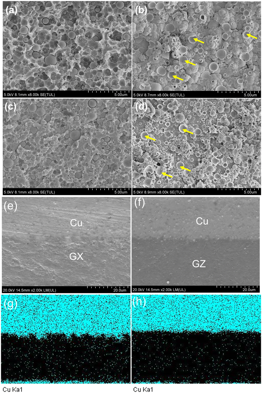 | ||
| Fig. 4 The surface SEM images of the film and copper after peeling: (a) GX film and (b) planted copper; (c) GZ film and (d) plated copper. Cross section SEM images of (e) GX and (f) GZ samples; EDS elemental mappings of (g) GX and (h) GZ samples. | ||
In order to further verify the above idea, energy dispersive spectroscopy (EDS) is beneficial to characterize the elemental distribution. Fig. 5a shows the elemental distribution on the surface of the GX film. It was clearly found that carbon, oxygen and silicon elements are detected on the surface of the GX film, and at the same time a small amount of copper is observed on the ABF surface. Fig. 5b shows the elemental distribution on the surface of the copper plated GX film. It can be seen that in addition to a large amount of copper element, we can also find some other elements such as carbon, oxygen and silicon elements. These results indicate that the adhesion failure does not occur at the interface, but inside the epoxy resin. Besides, the elemental distribution on the surface of the GZ film and copper layer is shown in Fig. 5c and d. As seen from the two results, we can find that in addition to carbon, oxygen and silicon elements, the surface of the GZ film has a small amount of copper element, and the loading content of copper is obvious lower than that of the former, while the surface of the copper plated GZ film also has some elemental distribution of carbon, oxygen and silicon as well as copper element. The elemental content of GX and GZ films and their corresponding copper surfaces are shown in Fig. 5e. By comparing the content of copper between GX and GZ films, we can find that the copper loading of the GX film is obviously higher than that of the GZ film, which is mainly attributed to the presence of more copper atoms entering into gaps between the GX film and silica particle. At the same time, it was also found that the total loading of elemental distribution of carbon, oxygen and silicon on the copper surface in the GZ film is also lower than that of the copper surface in the GX film, which indicates that the interaction force between the GX film and copper is stronger than that between the GZ film and copper.
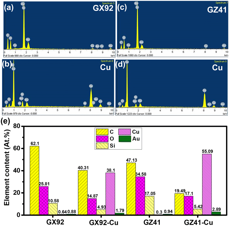 | ||
| Fig. 5 Elemental distribution pattern on the surface of ABF and copper layer after peeling: (a) GX film; (b) copper plated GX film; (c) GZ film; (d) copper plated GZ film; (e) comparison of element contents. | ||
In order to further analyze the effect of the surface roughness of the film surface on the interfacial adhesion strength between copper and ABF, the surface roughness of the film was tested with an interference microscope. The area with about 303 μm × 253 μm of sample surface is scanned. Fig. S5a and S5b† show the surface roughness morphology of GX and GZ films before copper plating. The average surface roughness of GX and GZ films is 316 and 163 nm, respectively. This result indicates that the removal of inner epoxy resin from the GZ film is different to the GX film, which is attributed to the GZ film having a high Young's modulus (9 GPa) and high glass transition temperature (198 °C) in comparison to those of the GX film (5 GPa vs. 168 °C) according to a previous literature report,7 which results in a huge challenge in the desmear process and a decrease in surface roughness, and this result is in accordance with that of Fig. S4a.† Fig. S5c and S5d† show the surface roughness morphology of GX and GZ films after peeling. It was found that the red area of the GX film has a high height (4.2 μm) and a low density of distribution in comparison to that of the GZ film (Fig. S5d†), and the corresponding surface roughness (Ra) of GX and GZ films is 442 nm and 308 nm. The reason of the increase of surface roughness in GX and GZ after peeling is that breaking of the epoxy matrix can happen in the inner ABF during the peeling process.
In addition to mechanical anchoring action, adhesion strength is also closely related to chemical interactions. In order to investigate the interfacial chemical interactions, the surface chemistry state was characterized by X-ray photoelectron spectroscopy (XPS).41,42 Herein, the XPS survey spectra of the initial and peeled samples as well as copper strip surfaces are shown in Fig. S6–S8.† It was clearly observed that the surface of the initial GX and GZ films consists of carbon and oxygen elements (see Fig. S6†), and while the surfaces of GX and GZ samples and their corresponding copper samples consist of carbon, oxygen and copper elements (see Fig. S7 and S8†). In the XPS survey spectrum, the peaks at 76.15 eV, 122.67 eV, 284.56 eV, (529.94 eV, 568.86 eV and 649.02 eV), 929.98 eV and 952.91 eV are assigned to Cu 3p, Cu 3s, C 1s, O 1s, Cu LMM, Cu 2p3/2 and Cu 2p1/2, respectively. In addition, it is worth noting that when copper is peeled from the surface of GX and GZ films, the fresh surfaces of copper and films all have the same element types, which indicates that the fracture occurs in the inner copper oxide and film. In order to further analyze the surface chemistry state, the C 1s and O 1s peaks of the initial and peeled GX and GZ films as well as their corresponding peeled copper surfaces are analyzed. Fig. S9a and S9b† show the C 1s XPS spectra of as-prepared GX and GZ films. For as-prepared GX films, the C 1s peak can be divided into three peaks at 284.7 eV, 286.3 eV, and 288.7 eV. And for as-prepared GZ, the C 1s peak also can be divided into three peaks at 284.7 eV, 286.3 eV and 289.0 eV. The peaks at 284.7 eV, 286.3 eV, and 288.7 eV are attributed to C–C and C–H, C–O–C and C![[double bond, length as m-dash]](https://www.rsc.org/images/entities/char_e001.gif) O groups, respectively. From fitting results, the peak area of each fitting peak can be calculated by Origin software. From the fitting results, it was found that the ratios of CO groups from the surface of initial GX and GZ films are 4.9% and 4.3%, respectively. Fig. S9c and S9d† show the C 1s XPS spectra of peeled GX and GZ films, and the ratios of CO groups are increased from 4.9 to 22.6% for the GX film, and from 4.3 to 12.3% for the GZ film, respectively. At the same time, the ratios of C–O–C groups of GX and GZ films are obviously decreased. The reason is that the C–O–C group can break under the oxidation of potassium permanganate, and generate the CO group and C–H group, which indicates that chemical interactions between the copper and film surface are increased by the desmearing process. Fig. S8† shows the C 1s XPS spectra of the fresh surface of the copper strip. It was found that there are some carbon and oxygen elements on the fresh surface of copper strips, indicating that copper reacts with some polar groups such as hydroxyl (–OH) and carboxyl (–COOH) groups, because copper does not react with carbon elements.43
O groups, respectively. From fitting results, the peak area of each fitting peak can be calculated by Origin software. From the fitting results, it was found that the ratios of CO groups from the surface of initial GX and GZ films are 4.9% and 4.3%, respectively. Fig. S9c and S9d† show the C 1s XPS spectra of peeled GX and GZ films, and the ratios of CO groups are increased from 4.9 to 22.6% for the GX film, and from 4.3 to 12.3% for the GZ film, respectively. At the same time, the ratios of C–O–C groups of GX and GZ films are obviously decreased. The reason is that the C–O–C group can break under the oxidation of potassium permanganate, and generate the CO group and C–H group, which indicates that chemical interactions between the copper and film surface are increased by the desmearing process. Fig. S8† shows the C 1s XPS spectra of the fresh surface of the copper strip. It was found that there are some carbon and oxygen elements on the fresh surface of copper strips, indicating that copper reacts with some polar groups such as hydroxyl (–OH) and carboxyl (–COOH) groups, because copper does not react with carbon elements.43
In order to verify the result that some polar groups react with copper and form the chemical interaction between copper and film, the interface between the film and copper layer was analyzed by the XPS depth profile. Fig. S10a and S10b† show the O 1s XPS spectra of as-prepared GX and GZ films. It was found that the O 1s peak of as-prepared GX and GZ films is only divided into two peaks which are assigned to C–O and CO bonds of polymer chains, and while the O 1s XPS spectra of the desmeared GX (Fig. S10c†) and GZ films (Fig. S10d†) are divided into four peaks which are assigned to H–O–H for water, C–O/CO for carbonyl groups, alcohol and ether groups, as well as Cu2O and CuO, respectively. Based on the above results, we can observe that the conditions for sample storage can affect the surface chemistry state of XPS, as H–O–H bonds are derived from adsorbed water vapor. In addition, we can also obverse that the total area ratios of C–O/CO bonds are decreased obviously, and meanwhile the O 1s peak becomes boarder and shifts to the low binding energy direction, which indicated that there is a chemical reaction between polar groups such as hydroxyl (–OH) and carboxyl (–COOH) groups and the metal copper layer, and then form copper oxide (CuO) and cuprous oxide (Cu2O) at the interface area based on the result of Fig. S11,† and this result is also consistent with a previous report.44
Although two kinds of samples both can form chemical bonds between copper and polar groups at the interfaces, their peel strengths are obviously different. To further study the difference in peel strength, the Cu 2p XPS spectra of the copper strip on the surface of GX and GZ films are shown in Fig. 6a. As can be seen, the peaks at 932.5 eV and 952.4 eV are assigned to Cu 2p3/2 and Cu 2p1/2, while the peaks at 941.3 eV and 943.5 eV, as well as 962.2 eV are satellite peaks of Cu2p3/2 and Cu2p1/2. These satellite peaks are derived from the main Cu 2p3/2 peak in CuO (while this satellite is absent for Cu and Cu2O) and the main Cu 2p1/2 peak in Cu2O, respectively.45,46 The reason for this phenomenon is explained in a molecular orbital description by a charge transfer mechanism. The above result is also consistent with previous reports. In addition, this result also further verified that there exist CuO and Cu2O at the interface areas, and based on the electron structure of Cu2O and CuO,47 the peaks at 933.1 eV and 932.2 eV are assigned to CuO and Cu2O. The main Cu 2p3/2 peaks are divided into three peaks, as shown in Fig. 6b and c. Based on a literature report,48 the middle peak is assigned to Cu2O, and the low binding energy peak is assigned to pure Cu, while the high binding energy peak is assigned to CuO. Based on the fitted results, it was found that the relative area ratios of Cu, CuO and Cu2O on the surface of the copper strip peeled from the GX film are 29.7%, 64.2% and 6.1%, while the relative area ratios of Cu, CuO and Cu2O on the surface of the copper strip peeled from the GZ film are 15.3%, 42% and 42.7%, respectively. Based on these results, it was clearly observed that the total content (70.3%) of copper oxides (CuO and Cu2O) at the interfaces between copper and the GX film is far lower than that (84.7%) of copper oxides (CuO and Cu2O) at the interfaces between copper and the GZ film, indicating that the interface areas of GZ films have more impurity phases which act as a weak boundary layer that is harmful to interface adhesion forces between copper and polymer composites. Therefore, the adhesion force of the GX sample is higher than that of the GZ sample. According to these results, we think that adhesion failure occurs in the inner copper oxide layer and polymer composites, and the adhesion failure mechanism is shown in Fig. 6d.
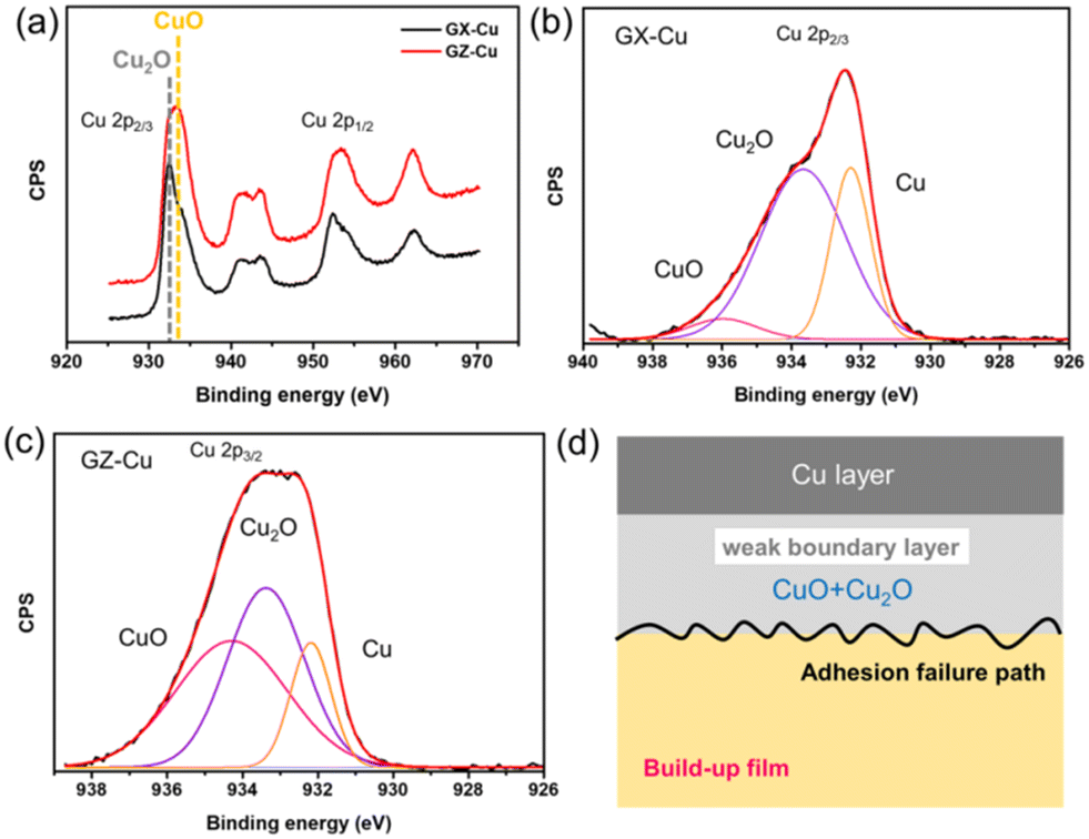 | ||
| Fig. 6 Cu 2p XPS spectra and adhesion failure mechanism: (a) Cu 2p peak of peeled copper strips; (b) Cu 2p3/2 of the GX film; (c) Cu 2p3/2 of the GZ film; (d) schematic diagram of the adhesive failure interface between copper and the polymer composite. | ||
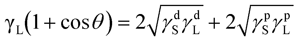
In order to calculate the adhesion work of the heterointerface between copper and polymer composites, the surface wettability of the initial and desmeared samples was measured from the static contact angle with water and ethanol. The static contact angles of the samples are shown in Fig. S12 and Table S1.† It was found that the contact angles of desmeared ABF are decreased obviously in comparison to those of the initial samples, indicating that the desmearing process can obviously enhance the surface wettability of sample surfaces because potassium permanganate acts as a strong oxidant that attacks the C–C or C–O bonds of polymer chains. These bonds can break and generate some polar groups on the surface of samples. In addition, the contact angle also can be used to analyze the polar ability of samples and work of adhesion of interfaces between ABF and copper. The work of adhesion can be calculated using the Young's equation and Dupre equation:48
| γSL = γS − γLcosθ | (1) |
| Wa = γS + γL − γSL = γL(1 + cosθ) | (2) |
| γ = γd + γp | (3) |
 | (4) |
Conclusions
In summary, we fabricated two chip substrates with four layers consisting of two ABFs (GX and GZ), copper and a commercial clad laminate by the wet chemistry method to study the interfacial adhesion mechanism. The surface roughness, surface microstructure and components of the samples were observed by interference microscopy and SEM, while the surface chemistry state and static contact angle of the samples were measured by XPS and static contact angle measurements. The above results showed that the difference in adhesion properties of the two kinds of chip substrates is mainly derived from the following four aspects: (1) the surface roughness of the GX film is higher than that of the GZ film, because the epoxy resin in the GX film is oxidized easily in comparison to that of the GZ film; (2) there are more additional anchoring points lying in gaps between the silica particle and epoxy resin for the GX film; (3) the content of impurity phases (CuO and Cu2O) for the GZ sample at interface areas is higher than that of the GX sample, because these impurity phases will play a dominant role in the weak boundary layer that can decrease the adhesion property; (4) the work of adhesion of hetero-interfaces between copper and the GX film is obviously higher than that of hetero-interfaces between copper and the GZ film, because the surface energy of the desmeared GX film is close to that of pure copper in comparison to the surface energy of the desmeared GZ film. This work will provide a direction for improving the adhesion forces of hetero-interfaces of chip substrates in the future.Conflicts of interest
The authors declare no competing interests.Acknowledgements
This work was supported by the Strategic Priority Research Program of Chinese Academy of Sciences (Grant No. XDA0330200) and the Postdoctoral Fellowship Program of CPSF (Grant No. GZC20232923).Notes and references
- L. C. Hung, P. I. Wu, H. C. Kuo, M. F. Jhong, C. C. Wang and S. M. Wang, IEEE CPMT Sym. Jap., 2022, pp. 134–137 Search PubMed.
- M. Töpper, A. Ostmann, T. Braun and K. D. Lang, Adv. Embed. Fan-Out Wafer-Level Pack. Technol., 2019, pp. 1–38 Search PubMed.
- S. C. Hsieh, F. C. Chu, C. Y. Ho and C. C. Wang, 22nd Eur. Microelectro. Pack. Conf Exhib., 2019, pp. 1–4 Search PubMed.
- I. Hu, J. C. Tsai, F. Cheng, S. F. Yen, M. K. Shih, D. Tarng, B. Pai and C. P. Hung, IEEE 21st Electron. Pack. Technol. Conf., 2019, pp. 467–471 Search PubMed.
- D. Hironiwa, Y. Morikawa, A. Ihori and R. Kamimura, IEEE 72nd Electron. Comp. Technol. Conf., 2022, pp. 862–866 Search PubMed.
- S. J. Ding, Z. D. Fang, Z. Y. Yu and Q. D. Wang, Mater. Today Commun., 2023, 37, 107201 CrossRef CAS.
- S. Fujishima and H. Sakauchi, Int. Conf. Electron. Pack., 2017, pp. 337–340 Search PubMed.
- S. Tatsumi, IEEE CPMT Sym. Jap., 2022, pp. 111–114 Search PubMed.
- S. Ikehira, IEEE 71st Electron. Comp. Technol. Conf., 2021, pp. 729–735 Search PubMed.
- M. Töpper, A. Ostmann, T. Braun and K. D. Lang, Adv. Embed. Fan-Out Wafer-Level Pack. Technol., 2019, pp. 1–38 Search PubMed.
- C. Y. Peng, J. H. Lau, C. T. Ko, P. Lee, E. Lin, H. K. M. Yang, P. B. Lin, T. Xia, L. Chang, T. N. Lee, J. Wong, M. Ma and T. J. Tseng, IEEE CPMT Sym. Jap., 2021, pp. 5–8 Search PubMed.
- T. Muguruma, A. Behr, H. Saito, K. Kishino, F. Suzuki, T. Shin and H. Umehara, IEEE 72nd Electron Comp. Technol. Conf., 2022, pp. 56–61 Search PubMed.
- K. Iwashita, T. Katoh, A. Nakamura, Y. Murakami, T. Iwasaki, Y. Sugimasa, J. Nunoshige and H. Nakano, J. Photopolym. Sci. Technol., 2015, 28, 93–97 CrossRef CAS.
- S. J. Ding, Z. D. Fang, Z. Y. Yu and Q. D. Wang, ACS Omega, 2023, 8, 32907–32916 CrossRef CAS.
- L. Granado, S. Kempa, L. J. Gregoriades, F. Brüning, T. Bernhard, V. Flaud, E. Anglaret and N. Fréty, ACS Appl. Electron. Mater., 2019, 1, 1498–1505 CrossRef CAS.
- J. Zhang, T. Li, H. P. Wang, Y. Liu and Y. F. Yu, Microelectron. Reliab., 2014, 54, 619–628 CrossRef CAS.
- T. Murayama, T. Sakuishi and Y. Morikawa, Int. Conf. Electron. Pack., 2019, pp. 246–250 Search PubMed.
- T. Thomas, PhD, Freie Universität Berlin, 2016 Search PubMed.
- Y. Oh, E. J. Kim, Y. Kim, K. Choi, W. B. Han, H. S. Kim and C. S. Yoon, Thin Solid Films, 2016, 600, 90–97 CrossRef CAS.
- J. Y. Sun, D. H. Hong, K. O. Ahn, S. H. Park, J. Y. Park and Y. H. Kim, J. Electrochem. Soc., 2013, 160, D107 CrossRef CAS.
- S. Homma, Y. Takano, T. Watanabe, K. Murakami, M. Fukuda, T. Imoto and H. Nishikawa, Mater. Trans., 2022, 63, 766–775 CrossRef CAS.
- C. Nair, F. Pieralisi, F. H. Liu, V. Sundaram, U. Muehlfeld, M. Hanika, S. Ramaswami and R. Tummala, IEEE 65th Electron. Comp. Technol. Conf., 2015, pp. 2248–2253 Search PubMed.
- P. Nimbalkar, C. Blancher, M. Kathaperumal, M. Swamin and R. Tummala, IEEE Trans. Device Mater. Reliab., 2022, 22, 59–64 CAS.
- Y. Oh, E. J. Kim, Y. Kim, K. Choi, W. B. Han, H. S. Kim and C. S. Yoon, Thin Solid Films, 2016, 600, 90–97 CrossRef CAS.
- S. Lee, W. Y. Jung, C. W. Ma, D. S. Lee, Y. H. Jung, D. S. Lee, Y. H. Jung, D. S. Lee, S. W. Han, E. C. Ahn, Y. H. Shin, H. S. Lee, H. J. Lim and I. S. Hwang, IEEE 21st Electron. Pack. Technol. Conf., 2019, pp. 271–275 Search PubMed.
- S. Kempa, W. Friz, F. Gaul, E. Habig and L. J. Gregoriades, Int. Microelectron. Assembly Pack. Soc., 2018, 2018, pp. 000634–000639.
- C. M. Wang, L. M. Zeng, W. C. Din and T. X. Liang, Vacuum, 2021, 191, 110330 CrossRef CAS.
- Y. Hong, X. Q. You, Y. Zeng, Y. M. Chen, Y. Z. Huang, W. Hem, S. X. Wang, C. Wang, G. Y. Zhou, X. H. Su and W. H. Zhang, Vacuum, 2019, 170, 108967 CrossRef CAS.
- P. T. Lee, C. H. Chang, C. Y. Lee, Y. S. Wu, C. H. Yang and C. E. Ho, Mater. Des., 2021, 206, 109830 CrossRef CAS.
- P. T. Lee, Y. S. Wu, C. Y. Lee, H. C. Liu and C. E. Ho, J. Electrochem. Soc., 2018, 165, D647 CrossRef CAS.
- P. T. Lee, Y. S. Wu, P. C. Lin, C. C. Chen, W. Z. Hsieh and C. E. Ho, Surf. Coat. Technol., 2017, 320, 559–567 CrossRef CAS.
- T. Fujinaga, IEEE 65th Electron. Comp. Technol. Conf., 2015, pp. 362–366 Search PubMed.
- D. Sadohara and C. E. J. Cordonier, Application of a Silicon Oligomer Coating As an Alternative Treatment to Substrate Surface Activation By Etching, Electrochemical Society Meeting Abstracts 236, The Electrochemical Society, Inc., 2019, (18), p. 1000 Search PubMed.
- A. Beyer, L. J. Gregoriades, S. Kempa, J. Lehmann and Y. Welz, 15th Int. Microsyst. Pack Assembly Circuit. Technol. Conf., 2020, pp. 185–187 Search PubMed.
- Y. Kitahara and J. Kang, Int. Conf. Electron. Pack., 2019, pp. 155–158 Search PubMed.
- J. C. Cho, H. Y. Lee, S. T. Lim, M. S. Park, Y. S. Oh, M. S. Cho and Y. K. Lee, Macromol. Res., 2010, 18, 47–52 CrossRef CAS.
- Y. Takagi, Y. Gunjo, H. Toyoda and H. Sugai, Vacuum, 2008, 83, 501–505 CrossRef CAS.
- Y. W. Huang, Y. P. Hung, R. S. Cheng, T. C. Chang, C. K. Lee and T. H. Chen, 5th Int. Microsyst. Pack. Assembly Circuit Technol. Conf., 2010, pp. 1–4 Search PubMed.
- M. S. Park, J. C. Cho, S. H. Kim, D. J. Shin, H. M. Jung, C. K. Lee, M. S. Cho and Y. Lee, Int. J. Adhes. Adhes., 2011, 31, 466–472 CrossRef CAS.
- J. Wang, MPhil, University of Electronic Science and Technology of China, 2022 Search PubMed.
- Y. Wang, L. J. Ni, F. Yang, F. Q. Gu, K. Liang, K. Marcus, Y. D. Wan, J. J. Chen and Z. S. Feng, J. Mater. Chem. C, 2017, 5, 12769–12776 RSC.
- S. J. Ding, G. C. Zhu, S. Zhao, L. Zhou and Y. J. Luo, Mater. Today Chem., 2023, 27, 101278 CrossRef CAS.
- Y. D. Chung, C. N. Whang, W. J. Lee, Y. S. Lee, S. K. Rha, Y. J. Lee and K. Y. Lim, Appl. Surf. Sci., 2003, 205, 128–136 CrossRef.
- W. J. Lee and Y. B. Kim, Thin Solid Films, 2008, 517, 1191–1194 CrossRef CAS.
- K. Cho and E. C. Cho, J. Adhes. Sci. Technol., 2000, 14, 1333–1353 CrossRef CAS.
- N. Pauly, S. Tougaard and F. Yubero, Surf. Sci., 2014, 620, 17–22 CrossRef CAS.
- J. Chijsen and L. H. Tjeng, Phys. Rev. B: Condens. Matter Mater. Phys., 1988, 38, 11322 CrossRef.
- F. Awaja, M. Gilbert, G. Kelly, B. Fox and P. J. Pigram, Prog. Polym. Sci., 2009, 34, 948–968 CrossRef CAS.
- J. Comyn, Int. J. Adhes. Adhes., 1992, 12, 145–149 CrossRef CAS.
- A. Royaux, A. E. Haitami, O. Fichet and S. Cantin, SN Appl. Sci., 2020, 2, 1–9 Search PubMed.
Footnote |
| † Electronic supplementary information (ESI) available: EDS, XPS, contact angle, surface energy of water and ethanol. See DOI: https://doi.org/10.1039/d4lf00153b |
| This journal is © The Royal Society of Chemistry 2024 |