
 Open Access Article
 This Open Access Article is licensed under a
 Creative Commons Attribution 3.0 Unported Licence
(F5PhO)2-F16-SiPc as an air-stable, high-performance n-type semiconductor with poor cannabinoid sensing capabilities†
Halynne R.
Lamontagne
 ab,
Mélanie
Cyr
ab,
Mário C.
Vebber
a,
Sufal
Swaraj
c,
Cory S.
Harris
d,
Jaclyn L.
Brusso
b,
Adam J.
Shuhendler
bde and
Benoît H.
Lessard
*af
ab,
Mélanie
Cyr
ab,
Mário C.
Vebber
a,
Sufal
Swaraj
c,
Cory S.
Harris
d,
Jaclyn L.
Brusso
b,
Adam J.
Shuhendler
bde and
Benoît H.
Lessard
*af
aDepartment of Chemical and Biological Engineering, University of Ottawa, 161 Louis Pasteur, Ottawa, ON K1N 6N5, Canada. E-mail: Benoit.Lessard@uottawa.ca
bDepartment of Chemistry and Biomolecular Sciences, University of Ottawa, 150 Louis Pasteur, Ottawa, ON K1N 6N5, Canada
cSOLEIL, L'Orme des Merisiers, Départementale 128, Saint-Aubin – 91190, France
dDepartment of Biology, University of Ottawa, 30 Marie Curie, Ottawa, ON K1N 6N5, Canada
eUniversity of Ottawa Heart Institute, 40 Ruskin St, Ottawa, ON K1Y 4W7, Canada
fSchool of Electrical Engineering and Computer Science, University of Ottawa, 800 King Edward Ave, Ottawa, ON K1N 6N5, Canada
First published on 14th June 2024
Abstract
Organic thin-film transistors (OTFTs) are an emerging platform for rapid, point-of-source detection and speciation of Δ9-tetrahydrocannabinol (THC) and cannabidiol (CBD). (F5PhO)2-F16-SiPc semiconductor was implemented into high performance, air-stable n-type bottom gate, bottom contact OTFTs, however, the resulting device performance changes in response to THC and CBD were negligible. We explored the orientation of the corresponding thin films by synchrotron-based grazing incidence wide-angle X-ray scattering (GIWAXS) and angle-dependent near-edge X-ray absorption fine structure (NEXAFS), as well as polarized Raman microscopy. These techniques demonstrate for the first time that (F5PhO)2-F16-SiPc molecules are at a 45–48° orientation to the substrate; comparable to other reported R2-SiPcs. This orientation did not change upon exposure to THC and CBD, which has previously been reported for phthalocyanine-based OTFT cannabinoid sensors. The presence of two bulky axial groups, along with the absence of hydrogens in the molecule and the low reactivity of the silicon atom likely causes the lack of interaction with the cannabinoids. While (F5PhO)2-F16-SiPc may be a successfully air-stable n-type semiconductor for OTFTs, the structural changes performed to make it air stable over traditional non-fluorinated silicon MPcs, are likely responsible for its lack of response to cannabinoid exposure.
Introduction
Organic thin-film transistors (OTFTs) are an exciting platform for the detection of various chemical and biological analytes.1–5 Low temperature manufacturing and fine tuning of the semiconductor structure enable a wide breadth of highly sensitive and selective sensors. One interesting potential application for OTFT sensors is for the detection and speciation of Δ9-tetrahydrocannabinol (THC) and cannabidiol (CBD).6 As cannabis and its products are becoming increasingly legalized and regulated in countries around the world, it has become necessary to quickly and accurately predict cannabinoid content in a variety of source samples.7 Previously, our group has demonstrated that OTFT sensors, using metal phthalocyanines (MPcs) as the semiconductor, can effectively detect and differentiate THC and CBD in both solution and vapor samples.6,8–11 THC and CBD interact with the inner nitrogen ring and central metal of the MPc molecule,11 leading to unique recrystallization and film reorganization that drives the changes in device performance.8,11 The choice of peripheral functional groups or metal inclusion within the macrocycle of the MPc has a significant effect on this recrystallization and the sensor response.8,9,11,12 When using trivalent MPcs such as aluminum Pc (R-AlPc),8,10 the axial group can be optimized to enhance film interactions and the response to cannabinoids.12 In most cases, the use of divalent and trivalent MPcs as the semiconductor leads to p-type OTFT operation and hole transporting sensors, which result in a turn-off response upon exposure to cannabinoids. Silicon phthalocyanines (R2-SiPcs), are tetravalent MPcs that have demonstrated n-type behaviour, with good electron mobilities and operation in OTFTs13–17 and organic photovoltaics (OPVs).18–22 Our group has reported extensively on the fabrication of OTFTs using R2-SiPcs, with studies focused on contact engineering,23 dielectric interface engineering,14,24,25 thin film processing,14–16,26 axial group functionalization,16,17,24,27–29 and more.30–33 To date, R2-SiPcs have never been reported as the semiconductor in OTFT based cannabinoid sensors due to their poor air stability. Recently, we reported the air stable OTFT operation of fluorinated R2-SiPcs due to the increased electron withdrawing nature of the fluorine groups, deepening the LUMO level and increasing its air stability.13,21,27 Bis(pentafluorophenoxy) hexadecafluoro silicon(IV) phthalocyanine ((F5PhO)2-F16-SiPc)13 has demonstrated good air-stable n-type performance in OTFTs and is a promising candidate for further development.In this study, we explore the use of (F5PhO)2-F16-SiPc as the semiconductor in OTFT based cannabinoid sensors. The OTFT sensors did not respond to the presence of CBD or THC. Upon study of the thin films, including novel characterization of these materials, we demonstrate the surprising lack of change with exposure to cannabinoids.
Results and discussion
Transistor characterization
Bottom-gate bottom-contact (BGBC) devices were fabricated with a thermally evaporated 50 nm layer of (F5PhO)2-F16-SiPc as the semiconductor on octyl trichlorosilane (OTS)-functionalized SiO2 as the dielectric with Au electrodes (W = 10 mm, L = 10 μm) (Fig. 1a). F2-F16-SiPc was synthesized according to a previously reported literature procedure,27 and the axial functionalization to obtain (F5PhO)2-F16-SiPc was adapted from an original reaction by Vebber et al.13 During this synthesis, single crystal data was not able to be obtained.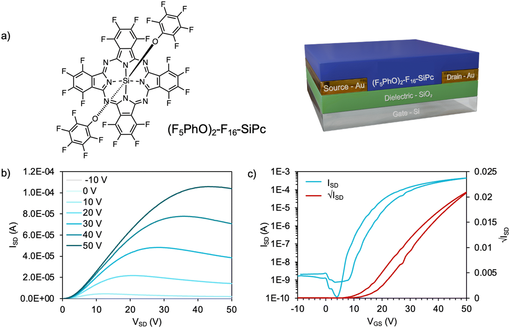 | ||
| Fig. 1 (a) (F5PhO)2-F16-SiPc chemical structure, and the bottom-gate bottom-contact (BGBC) device architecture used in this study, along with the associated (b) output curves and (c) transfer curves (VSD = 50 V) of the (F5PhO)2-F16-SiPc OTFTs tested in air. | ||
The output and transfer curves from a representative device tested in air are shown in Fig. 1b and c. The average electron mobility (μe) was 0.04 ± 0.01 cm2 V−1 s−1, with a threshold voltage (VT) of 9.9 V and a median on-current (IOn) of 0.32 mA, from a minimum of 20 transistors. These results surpass our previously recorded performance for (F5PhO)2-F16-SiPc in air (Table S1, ESI†), which were obtained in a bottom-gate top-contact (BGTC) architecture using Ag electrodes (W = 1 mm, L = 30 μm).13 The improved performance is likely due to the improved electrode architecture and electrode material. While BGBC architectures are generally associated with higher contact resistance and reduced performance, the increased W/L would lead to an increased overall channel surface area, improving μe and IOn, as charge could move through the channel more quickly.
The resulting (F5PhO)2-F16-SiPc OTFTs were exposed to THC and CBD vapor (Fig. 2). A substrate was also left out in air for the time taken to expose and test the other devices to compare any changes in performance to those experienced by air exposure (control). As shown in Fig. 2, negligible changes in transfer characteristics were observed, where changes in μe and VT were within statistical error of the controls. Unlike when using fluorinated copper MPc (F16-CuPc),6 another n-type semiconductor, the VT did not reliably decrease for both cannabinoids, which would be indicative of a turn-on response. However, the μe was found to decrease as it had for F16-CuPc, though not significantly more than what was experienced by the control. Interestingly, the defect density, N, for the exposed samples was shown to increase in relation to the air-only sample, indicating that exposure to cannabinoids potentially introduces additional charge traps to the film, which may help explain the slightly reduced μe. Regardless, we could not conclusively detect the cannabinoids using (F5PhO)2-F16-SiPc OTFTs.
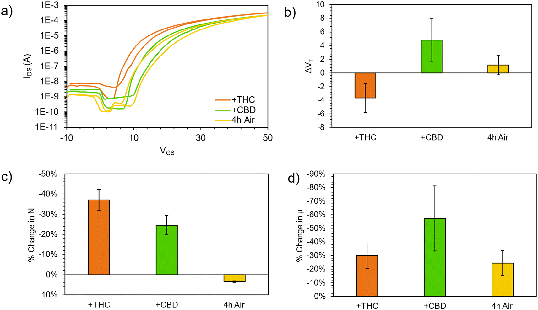 | ||
| Fig. 2 (F5PhO)2-F16-SiPc performance after exposure to THC and CBD, or after 4 h of air exposure as a control, demonstrated by the (a) transfer curve (VSD = 50 V) of a representative device, (b) average change in threshold voltage, VT, (c) average change in defect density, N, and (d) the average change in electron mobility, μe. All averages are for a minimum of 10 transistors. | ||
Thin-film characterization
Typically, MPc films experience significant changes in morphology and orientation when exposed to cannabinoid vapors or solutions.8–10,12 Therefore, (F5PhO)2-F16-SiPc films were characterized using various synchrotron based techniques, for the first time, to investigate if any morphological or orientational changes would occur upon exposure to cannabinoids. In the absence of single-crystal data, multiple techniques were used in combination to characterize the film structure.Angle-dependent near-edge X-ray absorption fine structure (NEXAFS) was performed at the carbon K-edge (280–310 eV) using monochromatic synchrotron X-ray beam polarized to linear horizontal (LH), where 50 nm films of (F5PhO)2-F16-SiPc on a SiN membrane were rotated between 0° and 60° with respect to the sample surface normal (Fig. 3). The rotation of the sample causes a change in the relative intensity of peaks in the NEXAFS spectra.34 By plotting the intensity of the peak associated with the  bonds in the SiPc macrocycle, we can determine if the majority of the molecules in the film are more face-on or edge-on by determining the dichroic ratio, R (Fig. 3d and e).35–38 In the NEXAFS spectrum of (F5PhO)2-F16-SiPc (Fig. 3a) there are four major features: (i) a peak at 285.6 eV associated with the 1 s to
  transition in unsaturated carbon bonds in the SiPc plane, (ii) a strong peak at 287.8 eV that can be attributed to the highly shifted
  from the fluorinated phenoxy substituents, (iii) a peak at 289 eV that is likely the highly shifted
  from the fluorinated substituents from the SiPc plane, and (iv) the multiple broad peaks above 293 eV associated with the 1 s to
  transitions.32 This spectra corresponds closely to that collected for (F5PhO)2-SiPc, with the addition of the signal at 289 eV for the additional peripheral fluorines.32 To determine the orientation of the SiPc macrocycle plane to the substrate surface, the intensity of the 285.6 eV signal was plotted against the angle of substrate rotation to generate a linear fit. This intensity increases with increasing angle of rotation, exhibiting dichroic behaviour and allowing the calculation of R, determined to be 0.26 for the baseline (F5PhO)2-F16-SiPc film (eqn (4)). This indicates a slight preference towards a pseudo edge-on orientation for molecules throughout the film, inclusive of both crystalline and amorphous regions. Edge-on orientation is preferred for OTFT applications, enabling charge transport through the film.
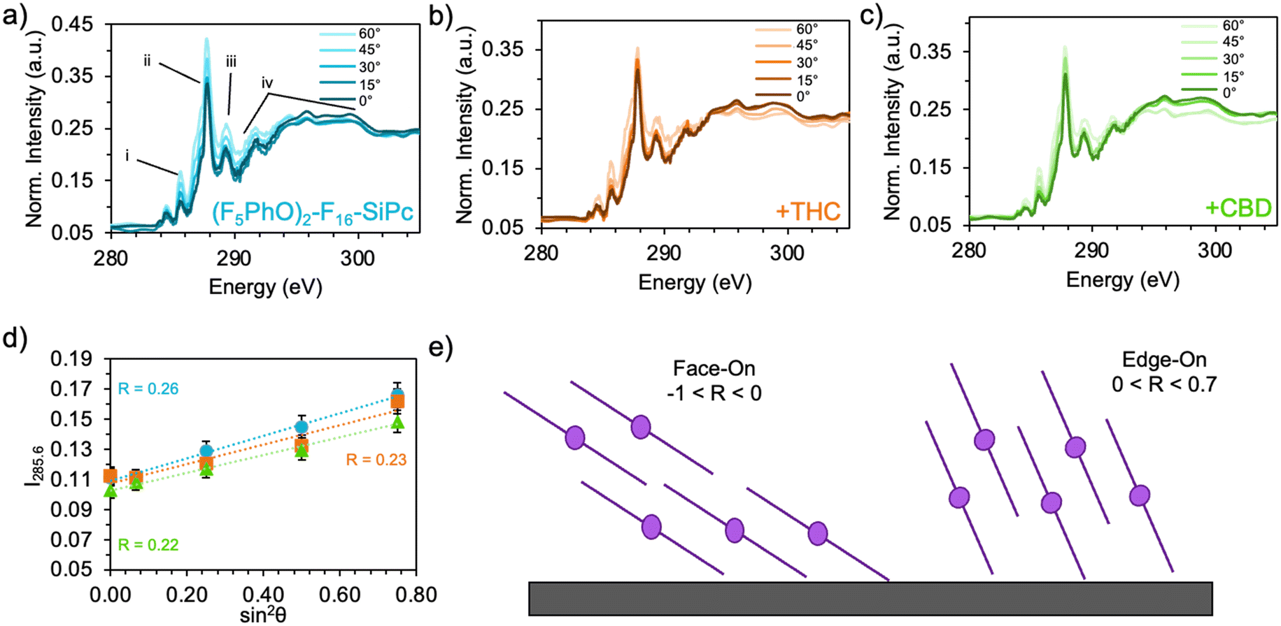 | ||
Fig. 3 (a) Normalized angle-dependent NEXAFS spectra for the baseline (F5PhO)2-F16-SiPc film, (b) after exposure to THC, and (c) after exposure to CBD. Features of the spectrum are highlighted by (i–iv). (d) The intensity of the peak of the 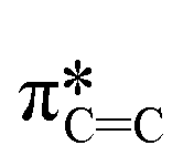 transition of the SiPc plane was plotted against sin2 transition of the SiPc plane was plotted against sin2![[thin space (1/6-em)]](https://www.rsc.org/images/entities/char_2009.gif) θ to generate a linear fit, allowing the calculation of the dichroic ratio, R, for each film, which indicates tendency towards face-on or edge-on orientation of the molecules to the surface, as shown in (e). θ to generate a linear fit, allowing the calculation of the dichroic ratio, R, for each film, which indicates tendency towards face-on or edge-on orientation of the molecules to the surface, as shown in (e). | ||
Angle-dependent NEXAFS was also performed on (F5PhO)2-F16-SiPc films after exposure to THC and CBD (Fig. 3b and c), where the same spectral features were observed, and the intensity of the  peak increased with increasing substrate rotation. The calculated R for the THC and CBD exposed samples was 0.23 and 0.22, respectively, indicating that the molecules remained primarily edge-on after cannabinoid exposure. Previous cannabinoid sensors, such as those fabricated with zinc Pc (ZnPc) and Cl-AlPc and its substituted derivatives, saw success due to their ability to adopt new polymorphs and crystal structures in films after exposure to cannabinoids.8–10,12 This small change in R experienced by (F5PhO)2-F16-SiPc indicates that this molecule does not undergo this same crystal rearrangement, and may be more stable in its thin film structure than other MPcs.
The (F5PhO)2-F16-SiPc films were also analyzed by polarized Raman microscopy, where Z(XX)Z′ and Z(XY)Z′ polarized Raman spectra were collected every 0.5 μm over a 10 × 10 μm area over the (F5PhO)2-F16-SiPc surface. The full baseline Raman spectrum can be found in Fig. S1 (ESI†). As we have previously demonstrated,26 we can use the ratio of intensities of the isoindole peak of the SiPc (∼1555 cm−1 in this case) at each polarization to find the average orientation of the SiPc molecule to the surface with eqn (3).26,39–43 The results were mapped on a contour plot (Fig. 4a–c), and the angle distribution plotted (Fig. 4d–f), showing an average molecular orientation of 47.8° to the surface for the baseline (F5PhO)2-F16-SiPc film (Fig. 4d). The distribution of average angles is tight, ranging from a minimum of 45.5° to a maximum of 49.5°. This is to be expected for a film deposited by physical vapor deposition, and is consistent with previous studies for vapor deposited R2-SiPcs, where angles between 44° and 52° have been found by polarized Raman microscopy.26 This calculated orientation is slightly more edge-on than face-on, supporting the NEXAFS results. Raman maps and angle distribution plots were also generated for the cannabinoid exposed samples (Fig. 4b, c, e and f), where the average angles were determined to be within standard deviation from the baseline sample. Again, this supports the NEXAFS results, indicating that (F5PhO)2-F16-SiPc films did not significantly change upon exposure to cannabinoids.
 | ||
| Fig. 4 Polarized Raman microscopy mapping on a 10 × 10 μm area with a 0.5 μm step size to generate a contour plot of the average (F5PhO)2-F16-SiPc angle to the surface, with the angle distribution for the (a and d) baseline (F5PhO)2-F16-SiPc film, (b and e) after exposure to THC, and (c and f) after exposure to CBD. | ||
Grazing-incidence wide-angle X-ray scattering (GIWAXS) is a useful technique to identify the molecular structure and crystallinity of MPc thin films. As seen in Fig. 5a–c, 2D GIWAXS spectra was obtained for the (F5PhO)2-F16-SiPc films, and the corresponding diffraction pattern was generated (Fig. 5d). The resulting pattern has very sharp, spot-like scattering features throughout, indicating a high level of crystallinity with narrow orientation distributions through the film; similar to what has been seen with (F5PhO)2-SiPc on OTS-treated substrates.24 The π–π stacking diffraction signal of MPcs attributed to the orientation of the central Pc plane is known to be associated with peaks in the upper q-range, around 1.7–2.1.9,10,16,24,25 Integration of the linecut profile of the GIWAXS spectra in a q-range of 1.7–1.9 (Fig. 5e), corresponding with the peak in the diffraction pattern indicated by (v) in Fig. 5d, gives a predominant (F5PhO)2-F16-SiPc angle of 45° to the substrate, with less intense peaks at 21°, 32°, 55°, and 83° indicating a mixed orientation film. These results agree with those observed by both Raman and NEXAFS, and are similar to those obtained previously for (F5PhO)2-SiPc on OTS by GIWAXS. Multiple orientations have been observed for other R2-SiPcs by GIWAXS, depending on their deposition technique and surface treatment,14,25 but the appearance of the more edge-on orientations of 45°, 55° and 83° is common for high-performing SiPcs like (F5PhO)2-SiPc, and causes improved horizontal charge transfer through the film, increasing the μe.14,24 In addition to the similar observed orientations, the d-spacing of the major peak in the diffraction pattern (Fig. 5d) commonly associated with the 010 and 001 planes of R2-SiPcs is nearly identical to that of (F5PhO)2-SiPc on OTS,24 at a q of 0.62 Å−1, indicating a similar packing structure and distance between molecules.
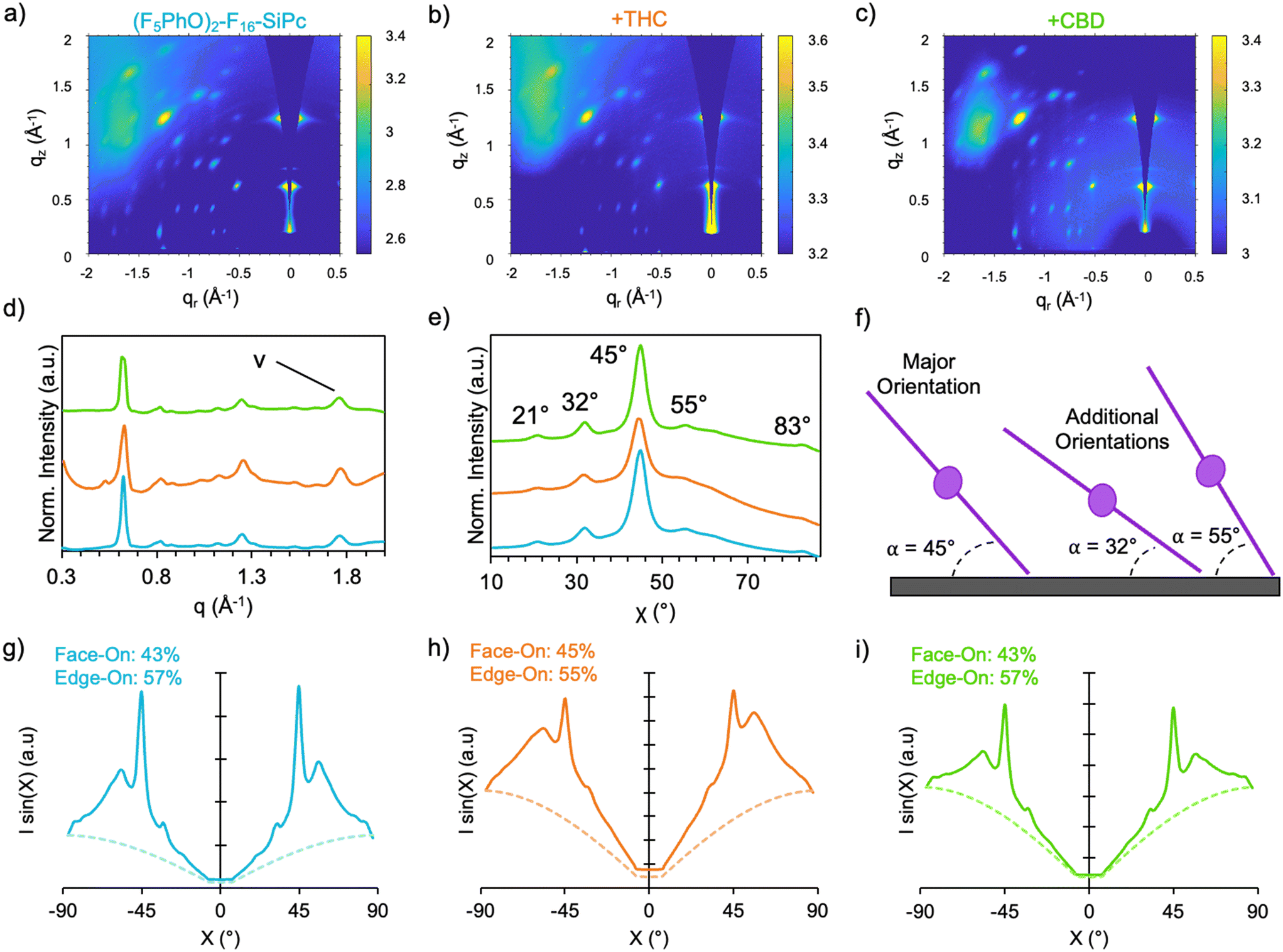 | ||
| Fig. 5 2D GIWAXS spectra and the corresponding geometrically corrected pole figure for (a and g) the baseline (F5PhO)2-F16-SiPc film, (b and h) after THC exposure, and (c and i) after CBD exposure. The pole figures were generated over the entire χ range, for a q-range of 1.7–1.9 to determine the proportion of edge-on and face-on crystallites in the film. The (d) diffraction pattern for each film and (e) non-corrected linecut profile with respect to χ for a q-range of 1.7–1.9 is shown, indicated by (v) in the diffraction pattern. The linecut profile identifies five prevalent molecular orientations, the most common are illustrated in (f). | ||
GIWAXS is a higher resolution technique than Raman and NEXAFS for identifying specific polymorphs and molecular angles, but it can only identify the orientation of molecules in crystalline regions of thin films that generate a diffraction pattern (not the amorphous regions), where Raman and NEXAFS identify average orientations through all regions of the film.44 To further quantify the orientation of these films by GIWAXS, the geometrically corrected pole figure was generated45–47 in the q-range from 1.7–1.9 (Fig. 5g), where the area under the curve was integrated to determine the population of face-on (<45°) and edge-on (>45°) molecules in the central Pc plane. For the baseline (F5PhO)2-F16-SiPc film, a 43% population of face-on molecules, and a 57% population of edge-on molecules was calculated. Again, these agree with the previous results from both NEXAFS and Raman, showing a slight preference toward edge-on orientation.
GIWAXS was also performed on (F5PhO)2-F16-SiPc films exposed to THC and CBD (Fig. 5b and c), and the same molecular orientations can be observed, with no significant new diffraction pattern indicating the appearance of new polymorphs. As previously mentioned, high performing MPc-based OTFT cannabinoid sensors have experienced significant film reorganization in response to cannabinoids, sometimes with the appearance of new polymorphs, and this has been observed through changes in orientation by GIWAXS.9,12 (F5PhO)2-F16-SiPc did not experience these types of changes in the molecular orientations, or in the relative intensity of these angles, which is consistent with the lack of significant change in device performance upon exposure. Additionally, the pole figures (Fig. 5h and i) did not show a significant change in the population of face-on and edge-on molecules in either of the exposed films.
In previous reports we have explored various MPcs as semiconductors in cannabinoid sensors and have found that the central atom plays a significant role in the sensitivity.8,11 For example, through solution based spectroelectrochemistry and 2D NMR experiments,11 along with thin film characterization,8 we have found that the central metal influences the film morphology and strength of analyte–MPc interactions, where ZnPc and R-AlPc resulted in the most sensitive devices.9,10,12 The fact that silicon is a relatively inert metalloid rather than a reactive metal, might contribute to the observed reduced interactions. The lack of response is likely not purely due to an energy mismatch from the use of an n-type material, as we have found success previously using the n-type F16-CuPc, resulting in a negative VT shift and reduction in μe.6
We have previously explored different levels of fluorination in ZnPcs with 0, 4, and 16 peripheral fluorine groups and found that while all were effective sensors, the unfluorinated ZnPc was the most sensitive, resulting in the greatest reduction in μh and the ability to detect 40 ppb THC vapor.9 This suggests that reducing the number of hydrogen groups available for hydrogen bonding and interacting with the cannabinoids may negatively impact its sensitivity, which helps to explain the observed reduced performance seen by (F5PhO)2-F16-SiPc.
Additionally, this work explores the first use of an R2-SiPc in a cannabinoid sensor, which is also the first report of a tetravalent MPc used in these sensors. We surmise the axial groups above and below the central silicon atom prevents significant interaction with the cannabinoid. As THC and CBD were found to primarily interact with the central ring of nitrogens in MPc molecules, the presence of bulky, inflexible axial groups on both sides of the central SiPc plane likely sterically hinder any potential cannabinoid interaction. It would appear that the structural changes required to make (F5PhO)2-F16-SiPc a semiconductor for air stable, n-type OTFT operation, has also made it resistant to interactions with cannabinoids, preventing its use as a sensing element.
Conclusion
We report the application of the air stable n-type semiconductor (F5PhO)2-F16-SiPc in BGBC OTFTs. We explored the corresponding thin films by synchrotron based GIWAXS and NEXAFS, as well as polarized Raman microscopy. These complimentary techniques demonstrate for the first time that the (F5PhO)2-F16-SiPc molecules are at a 45–48° angle from the substrate with relatively homogeneous morphology, which is comparable to the orientations previously found for (F5PhO)2-SiPc and other SiPcs. We also explored the use of (F5PhO)2-F16-SiPc based OTFTs as cannabinoid sensors and found no statistical difference in performance before and after exposure to CBD and THC. The film characterization also revealed negligible changes in structure with exposure to cannabinoids which has been reported for high performing MPc OTFT cannabinoid sensors. Overall, (F5PhO)2-F16-SiPc is among the most air-stable silicon based MPc used in OTFTs, but the very structural changes that lead to this air stability and high performance are what prevent its use as a cannabinoid sensing molecule.Experimental methods
Materials
Tetrafluorophthalonitrile (97%) and pentafluoro phenol (99%) were purchased from Ambeed. Lithium bis(trimethylsilylamide) (97%) was purchased from Sigma Aldrich and the etherate was prepared as outlined in literature.48 Silicon tetrachloride (99%), boron trichloride (1 M in heptane), anhydrous tetraline, chlorobenzene and (octyl)trichlorosilane (OTS, 97%) were purchased from Sigma Aldrich and used as received. All solvents used in device fabrication were HPLC grade and purchased from Fisher Scientific. Toronto Research Chemicals supplied the cannabinoid standards.Chemical synthesis
Thin-film deposition
Fraunhofer IPMS supplied custom prefabricated devices to make BGBC transistors, each consisting of a 230 nm thermally grown SiO2 dielectric layer on an Si gate, and prepatterned source-drain electrodes with a W/L of 1000 (W = 10 mm, L = 10 μm). Silicon (Si) substrates from WaferPro were used for GIWAXS sample preparation. The substrates were washed with acetone to remove the photoresist, then with isopropanol and dried under a N2 gas stream. They were then treated with oxygen plasma for 15 minutes, briefly rinsed with water, isopropanol, and dried with N2. Once dry, they were immersed in a 1% v/v OTS solution in toluene for 1 hour at 70 °C. The substrates were then rinsed with toluene and isopropanol, dried with N2, and placed in a vacuum oven at 70 °C for 1 hour to remove trace solvent. The substrates were placed in an Angstrom EvoVac thermal evaporator at a pressure below 2 × 10⁻⁶ Torr, where (F5PhO)2-F16-SiPc was deposited by sublimation at 0.2 Å s−1 until a thickness of 500 Å was reached.OTFT characterization
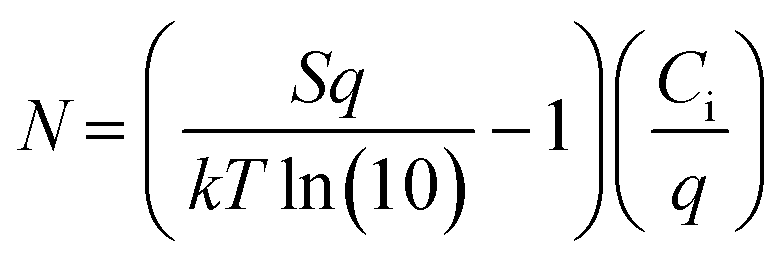
Transistors were tested using a custom-build auto tester machine and run using a Keithley 2614B SourceMeter and Labview software. The VDS and VGS were set and the ISD was measured to obtain both output and transfer curves. Five transfer curves were taken for each transistor and the final three were averaged. From the transfer curve, the VT, N and μe could be extracted, the latter using eqn (1), for saturation operation, where Ci is the capacitance.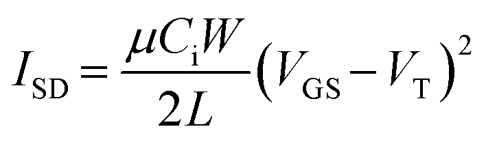 | (1) |
 | (2) |
GIWAXS characterization
Grazing incidence wide angle X-ray scattering (WAXS) data was collected using the Brockhouse X-ray Diffraction and Scattering (BXDS) low energy wiggler beamline (04ID-2).49 04ID-2 employed a Si(111) single side-bounce monochromator crystal to select a photon energy of ∼15.1 keV (wavelength = 0.81931 A). The beamline employs a Huber four-circle diffractometer end-station which was used to select grazing incidence angles of 0.1 and 0.3 degrees. The sample position was oriented using an automated, iterative procedure to scan the sample height and incidence (theta) angle. WAXS data was collected on a Rayonix MX300 CCD detector using a detector distance of ∼474 mm to obtain a Q value of 2. The sample-detector distance and tilt were calibrated using a silver behenate reference material. Samples and reference materials were collected with acquisition times ranging from 0.1 to 30 s. Silver behenate (AgBeh) standards were used to calibrate the data, and the data was analyzed using the GIXSGUI software package in MatLab.Polarized Raman microscopy and angle mapping
Thin films of (F5PhO)2-F16-SiPc were characterized by polarized Raman microscopy (Z(X,X)Z′ and Z(X,Y)Z′) on a Renishaw inVia Quontor confocal Raman microscope, which uses a Leica Microsystems bright field microscope with a DM2700 light source. A 500 mW 532 nm laser with a 2400 l mm−1 grating was used to collect spectra between 550 cm−1 and 1700 cm−1 at 5% laser power (25 mW) and an exposure time of 2 s. Individual spectra were taken every 0.5 μm over a 10 × 10 μm area at ×50L microscope magnification at both polarizations for a total of 441 spectra per polarization. With the objective and laser combination used, the Raman microscope has a spectral resolution of 0.3 cm−1 (FWHM), a theoretical spatial resolution of 640 nm, and a theoretical depth of focus of 3.0 um. Calibration was performed prior to all measurements against the 520 cm−1 silicon reference peak within 0.5 cm−1. The intensity of the Raman peak at 1555 cm−1, the B1g pyrrole stretch, was obtained by Wire 5.6 inVia software for both polarizations (IXX and IXY) was used to calculate the angle of the planar (F5PhO)2-F16-SiPc core using eqn (3).26,39–43 The resulting angles were then mapped on a contour plot using MatLab software. | (3) |
Near-edge X-ray absorption fine structure (NEXAFS)
Samples for near edge X-ray absorption fine structure (NEXAFS) were prepared on custom substrates purchased from NORCADA Inc with two transparent silicon nitride (SiN) membranes (0.10 mm × 0.25 mm, thickness = 50 nm) on a Si frame. The membranes were treated with oxygen plasma and OTS following the same procedure as transistor substrate preparation, followed by the deposition of 50 nm of (F5PhO)2-F16-SiPc, taking care to not damage the delicate membrane. After removal from the evaporator, the membranes were inspected for damage under a bright field microscope before NEXAFS characterization.NEXAFS experiments were conducted using a Research Instruments scanning transmission X-ray microscopy (STXM) apparatus, provided by RI Research Instruments GmbH, Germany, at the HERMES beamline50 at the synchrotron SOLEIL facility. A Fresnel zone plate with a 25 nm outer zone radius was used to focus a monochromatic X-ray beam onto the sample. The sample was attached to a stage capable of raster scanning and polar angle rotation. A photomultiplier tube (PMT) was used to detect the transmitted X-rays. Polarization switching was facilitated by automated adjustments of the undulators, all the while preserving beam alignment and flux. Throughout all measurements, the microscope chamber was held under vacuum at a pressure of 10−4 mbar. Energy data sets comprised of line scans were acquired at the carbon K-edge, from 280 to 310 eV. For each line scan a region of 5 μm length was scanned with step size of 250 nm and a dwell time of 100. The lines scans were repeated at various X-ray incident angles (θ) of 0°, 15°, 30°, 45°, and 60° with respect to the sample surface normal. The set up and rotation of sample has been detailed previously by our group.51
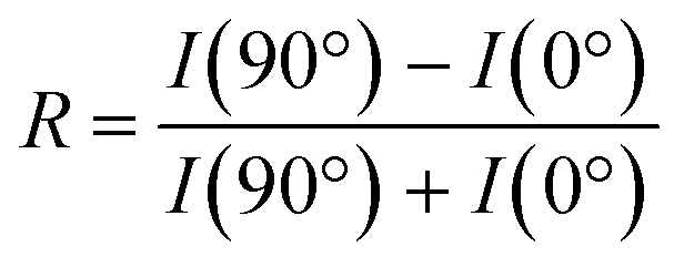
The dichroic ratio, R, was calculated using eqn (4), which is an indication of orientation tendency. I(90°) is determined using the linear fit from the plot of the intensity of the  signal (I285.6) against sin2θ.
 | (4) |
Data availability
The data that support the findings of this study are available from the corresponding author, BHL, upon reasonable request.Conflicts of interest
There are no conflicts to declare.Acknowledgements
This work was supported by NSERC Discovery grant RGPIN 2015-05796 (A. J. S.), 2015-05453 (C. S. H.), and 2020-04079 (B. H. L.), the Canada Research Chairs Program 950-230754 (A. J. S.) and 950-230724 (B. H. L.). Student support was acquired through NSERC PGS-D (H. R. L.) and CGS-D (M. C.). GIWAXS was performed at the Canadian Light Source, a national research facility of the University of Saskatchewan, which is supported by the Canada Foundation for Innovation (CFI), the Natural Sciences and Engineering Research Council (NSERC), the National Research Council (NRC), the Canadian Institutes of Health Research (CIHR), the Government of Saskatchewan, and the University of Saskatchewan. The authors would also like to thank Synchrotron SOLEIL for providing beamtime at the HERMES beamline for the NEXAFS characterization.References
- B. King and B. H. Lessard, Review of Recent Advances and Sensing Mechanisms in Solid-State Organic Thin-Film Transistor (OTFT) Sensors, J. Mater. Chem. C, 2024, 12(16), 5654–5683, 10.1039/D3TC03611A.
- P. Lin, F. Yan, P. Lin and F. Yan, Organic Thin-Film Transistors for Chemical and Biological Sensing, Adv. Mater., 2012, 24(1), 34–51, DOI:10.1002/ADMA.201103334.
- J.-H. Kwon, M.-H. Kim and J.-H. Bae, A Review on Diverse Streams of Interface Engineering for Organic Thin-Film Transistors, J. Mater. Chem. C, 2023, 12(1), 29–49, 10.1039/D3TC02712K.
- C. Sun and T. Wang, Organic Thin-Film Transistors and Related Devices in Life and Health Monitoring, Nano Res., 2024, 17(2), 426–444, DOI:10.1007/s12274-023-5606-1.
- M. Wu, S. Hou, X. Yu and J. Yu, Recent Progress in Chemical Gas Sensors Based on Organic Thin Film Transistors, J. Mater. Chem. C, 2020, 8(39), 13482–13500, 10.1039/D0TC03132A.
- Z. J. Comeau, N. T. Boileau, T. Lee, O. A. Melville, N. A. Rice, Y. Troung, C. S. Harris, B. H. Lessard and A. J. Shuhendler, On-the-Spot Detection and Speciation of Cannabinoids Using Organic Thin-Film Transistors, ACS Sens., 2019, 4(10), 2706–2715, DOI:10.1021/acssensors.9b01150.
- D. I. Abrams, The Therapeutic Effects of Cannabis and Cannabinoids: An Update from the National Academies of Sciences, Engineering and Medicine Report, Eur. J. Intern. Med., 2018, 49, 7–11, DOI:10.1016/J.EJIM.2018.01.003.
- Z. J. Comeau, N. A. Rice, C. S. Harris, A. J. Shuhendler and B. H. Lessard, Organic Thin-Film Transistors as Cannabinoid Sensors: Effect of Analytes on Phthalocyanine Film Crystallization, Adv. Funct. Mater., 2022, 32(7), 2107138, DOI:10.1002/adfm.202107138.
- Z. J. Comeau, R. R. Cranston, H. R. Lamontagne, C. S. Harris, A. J. Shuhendler and B. H. Lessard, Surface Engineering of Zinc Phthalocyanine Organic Thin-Film Transistors Results in Part-per-Billion Sensitivity towards Cannabinoid Vapor, Commun. Chem., 2022, 5(1), 1–8, DOI:10.1038/s42004-022-00797-y.
- H. R. Lamontagne, Z. J. Comeau, R. R. Cranston, N. T. Boileau, C. S. Harris, A. J. Shuhendler and B. H. Lessard, Chloro Aluminum Phthalocyanine-Based Organic Thin-Film Transistors as Cannabinoid Sensors: Engineering the Thin Film Response, Sens. Diagn., 2022, 1(6), 1165–1175, 10.1039/D2SD00071G.
- Z. J. Comeau, G. A. Facey, C. S. Harris, A. J. Shuhendler and B. H. Lessard, Engineering Cannabinoid Sensors through Solution-Based Screening of Phthalocyanines, ACS Appl. Mater. Interfaces, 2020, 12(45), 50692–50702, DOI:10.1021/acsami.0c17146.
- H. R. Lamontagne, R. R. Cranston, Z. J. Comeau, C. S. Harris, A. J. Shuhendler and B. H. Lessard, Axial Phenoxylation of Aluminum Phthalocyanines for Improved Cannabinoid Sensitivity in OTFT Sensors, Adv. Sci., 2024, 11(27), 2305515, DOI:10.1002/advs.202305515.
- B. King, M. C. Vebber, R. Ewenike, M. Dupuy, C. French, J. L. Brusso and B. H. Lessard, Peripherally Fluorinated Silicon Phthalocyanines: How Many Fluorine Groups Are Necessary for Air-Stable Electron Transport in Organic Thin-Film Transistors?, Chem. Mater., 2023, 35(20), 8517–8528, DOI:10.1021/acs.chemmater.3c01342.
- R. R. Cranston, M. C. Vebber, J. F. Berbigier, N. A. Rice, C. Tonnelé, Z. J. Comeau, N. T. Boileau, J. L. Brusso, A. J. Shuhendler, F. Castet, L. Muccioli, T. L. Kelly and B. H. Lessard, Thin-Film Engineering of Solution-Processable n-Type Silicon Phthalocyanines for Organic Thin-Film Transistors, ACS Appl. Mater. Interfaces, 2021, 13(1), 1008–1020, DOI:10.1021/ACSAMI.0C17657.
- R. R. Cranston, B. King, C. Dindault, T. M. Grant, N. A. Rice, C. Tonnelé, L. Muccioli, F. Castet, S. Swaraj and B. H. Lessard, Highlighting the Processing Versatility of a Silicon Phthalocyanine Derivative for Organic Thin-Film Transistors, J. Mater. Chem. C, 2022, 10(2), 485–495, 10.1039/D1TC05238A.
- R. R. Cranston, M. C. Vebber, J. Faleiro Berbigier, J. Brusso, T. L. Kelly and B. H. Lessard, High Performance Solution Processed N-Type OTFTs through Surface Engineered F–F Interactions Using Asymmetric Silicon Phthalocyanines, Adv. Electron. Mater., 2022, 8(12), 2200696, DOI:10.1002/aelm.202200696.
- B. King, A. J. Daszczynski, N. A. Rice, A. J. Peltekoff, N. J. Yutronkie, B. H. Lessard and J. L. Brusso, Cyanophenoxy-Substituted Silicon Phthalocyanines for Low Threshold Voltage n-Type Organic Thin-Film Transistors, ACS Appl. Electron. Mater., 2021, 3(5), 2212–2223, DOI:10.1021/acsaelm.1c00175.
- M.-T. Dang, T. M. Grant, H. Yan, D. S. Seferos, B. H. Lessard and T. P. Bender, Bis(Tri-n-Alkylsilyl Oxide) Silicon Phthalocyanines: A Start to Establishing a Structure Property Relationship as Both Ternary Additives and Non-Fullerene Electron Acceptors in Bulk Heterojunction Organic Photovoltaic Devices, J. Mater. Chem. A, 2017, 5(24), 12168–12182, 10.1039/C6TA10739G.
- T. M. Grant, D. S. Josey, K. L. Sampson, T. Mudigonda, T. P. Bender and B. H. Lessard, Boron Subphthalocyanines and Silicon Phthalocyanines for Use as Active Materials in Organic Photovoltaics, Chem. Rec., 2019, 19(6), 1093–1112, DOI:10.1002/tcr.201800178.
- B. H. Lessard, The Rise of Silicon Phthalocyanine: From Organic Photovoltaics to Organic Thin Film Transistors, ACS Appl. Mater. Interfaces, 2021, 13(27), 31321–31330, DOI:10.1021/ACSAMI.1C06060.
- B. H. Lessard, T. M. Grant, R. White, E. Thibau, Z.-H. Lu and T. P. Bender, The Position and Frequency of Fluorine Atoms Changes the Electron Donor/Acceptor Properties of Fluorophenoxy Silicon Phthalocyanines within Organic Photovoltaic Devices, J. Mater. Chem. A, 2015, 3(48), 24512–24524, 10.1039/C5TA07173A.
- M. C. Vebber, N. A. Rice, J. L. Brusso and B. H. Lessard, Thermodynamic Property–Performance Relationships in Silicon Phthalocyanine-Based Organic Photovoltaics, ACS Appl. Energy Mater., 2022, 5(3), 3426–3435, DOI:10.1021/acsaem.1c04013.
- O. A. Melville, T. M. Grant, K. Lochhead, B. King, R. Ambrose, N. A. Rice, N. T. Boileau, A. J. Peltekoff, M. Tousignant, I. G. Hill and B. H. Lessard, Contact Engineering Using Manganese, Chromium, and Bathocuproine in Group 14 Phthalocyanine Organic Thin-Film Transistors, ACS Appl. Electron. Mater., 2020, 2(5), 1313–1322, DOI:10.1021/acsaelm.0c00104.
- B. King, C. L. Radford, M. C. Vebber, B. Ronnasi and B. H. Lessard, Not Just Surface Energy: The Role of Bis(pentafluorophenoxy) Silicon Phthalocyanine Axial Functionalization and Molecular Orientation on Organic Thin-Film Transistor Performance, ACS Appl. Mater. Interfaces, 2023, 15(11), 14937–14947, DOI:10.1021/acsami.2c22789.
- R. B. Ewenike, B. King, A. M. Battaglia, J. D. Quezada Borja, Z. S. Lin, J. G. Manion, J. L. Brusso, T. L. Kelly, D. S. Seferos and B. H. Lessard, Toward Weak Epitaxial Growth of Silicon Phthalocyanines: How the Choice of the Optimal Templating Layer Differs from Traditional Phthalocyanines, ACS Appl. Electron. Mater., 2023, 5(12), 7023–7033, DOI:10.1021/acsaelm.3c01389.
- R. R. Cranston, T. D. Lanosky, R. Ewenike, S. Mckillop, B. King and B. H. Lessard, Polarized Raman Microscopy to Image Microstructure Changes in Silicon Phthalocyanine Thin-Films, Small Sci., 2024, 4(6), 2300350, DOI:10.1002/smsc.202300350.
- M. C. Vebber, B. King, C. French, M. Tousignant, B. Ronnasi, C. Dindault, G. Wantz, L. Hirsch, J. Brusso and B. H. Lessard, From P-Type to N-Type: Peripheral Fluorination of Axially Substituted Silicon Phthalocyanines Enables Fine Tuning of Charge Transport, Can. J. Chem. Eng., 2023, 101(6), 3019–3031, DOI:10.1002/cjce.24843.
- N. J. Yutronkie, B. King, O. A. Melville, B. H. Lessard and J. L. Brusso, Attaining Air Stability in High Performing N-Type Phthalocyanine Based Organic Semiconductors, J. Mater. Chem. C, 2021, 9(31), 10119–10126, 10.1039/D1TC02275J.
- B. King, O. A. Melville, N. A. Rice, S. Kashani, C. Tonnelé, H. Raboui, S. Swaraj, T. M. Grant, T. McAfee, T. P. Bender, H. Ade, F. Castet, L. Muccioli and B. H. Lessard, Silicon Phthalocyanines for N-Type Organic Thin-Film Transistors: Development of Structure–Property Relationships, ACS Appl. Electron. Mater., 2021, 3(1), 325–336, DOI:10.1021/acsaelm.0c00871.
- R. R. Cranston, M. C. Vebber, N. A. Rice, C. Tonnelé, F. Castet, L. Muccioli, J. L. Brusso and B. H. Lessard, N-Type Solution-Processed Tin versus Silicon Phthalocyanines: A Comparison of Performance in Organic Thin-Film Transistors and in Organic Photovoltaics, ACS Appl. Electron. Mater., 2021, 3(4), 1873–1885, DOI:10.1021/acsaelm.1c00114.
- S. Ganesh Moorthy, B. King, A. Kumar, E. Lesniewska, B. H. Lessard and M. Bouvet, Molecular Engineering of Silicon Phthalocyanine to Improve the Charge Transport and Ammonia Sensing Properties of Organic Heterojunction Gas Sensors, Adv. Sens. Res., 2023, 2(3), 2200030, DOI:10.1002/adsr.202200030.
- C. Dindault, B. King, P. Williams, J. H. Absi, M. D. M. Faure, S. Swaraj and B. H. Lessard, Correlating Morphology, Molecular Orientation, and Transistor Performance of Bis(pentafluorophenoxy)Silicon Phthalocyanine Using Scanning Transmission X-Ray Microscopy, Chem. Mater., 2022, 34(10), 4496–4504, DOI:10.1021/acs.chemmater.2c00277.
- B. King, S. G. Moorthy, E. Lesniewska, R. Meunier-Prest, M. Bouvet and B. H. Lessard, Modulating the Majority Charge Carrier Type and Performance of Organic Heterojunction Ammonia Sensors by Increasing Peripheral Fluorination of the Silicon Phthalocyanine Sublayer, Sens. Actuators, B, 2024, 408, 135507, DOI:10.1016/j.snb.2024.135507.
- A. Salleo, R. J. Kline, D. M. DeLongchamp and M. L. Chabinyc, Microstructural Characterization and Charge Transport in Thin Films of Conjugated Polymers, Adv. Mater., 2010, 22(34), 3812–3838, DOI:10.1002/adma.200903712.
- D. DeLongchamp, E. Lin and D. Fischer, Organic Semiconductor Structure and Chemistry from Near-Edge X-Ray Absorption Fine Structure (NEXAFS) Spectroscopy, in Proc. SPIE 5940, Organic Field-Effect Transistors IV, 59400A, San Diego, California, United States, DOI:10.1117/12.616776.
- T. Schuettfort, L. Thomsen and C. R. McNeill, Observation of a Distinct Surface Molecular Orientation in Films of a High Mobility Conjugated Polymer, J. Am. Chem. Soc., 2013, 135(3), 1092–1101, DOI:10.1021/ja310240q.
- M. G. Samant, J. Stöhr, H. R. Brown, T. P. Russell, J. M. Sands and S. K. Kumar, NEXAFS Studies on the Surface Orientation of Buffed Polyimides, Macromolecules, 1996, 29(26), 8334–8342, DOI:10.1021/ma951820c.
- J. Stöhr, M. G. Samant, J. Lüning, A. C. Callegari, P. Chaudhari, J. P. Doyle, J. A. Lacey, S. A. Lien, S. Purushothaman and J. L. Speidell, Liquid Crystal Alignment on Carbonaceous Surfaces with Orientational Order, Science, 2001, 292(5525), 2299–2302, DOI:10.1126/science.1059866.
- M. Szybowicz and J. Makowiecki, Orientation Study of Iron Phthalocyanine (FePc) Thin Films Deposited on Silicon Substrate Investigated by Atomic Force Microscopy and Micro-Raman Spectroscopy, J. Mater. Sci., 2012, 47(3), 1522–1530, DOI:10.1007/s10853-011-5940-7.
- M. Szybowicz, W. Bała, K. Fabisiak, K. Paprocki and M. Drozdowski, The Molecular Structure Ordering and Orientation of the Metallophthalocyanine CoPc, ZnPc, CuPc, and MgPc Thin Layers Deposited on Silicon Substrate, as Studied by Micro-Raman Spectroscopy, J. Mater. Sci., 2011, 46(20), 6589–6595, DOI:10.1007/s10853-011-5607-4.
- M. Szybowicz, W. Bała, K. Fabisiak, K. Paprocki and M. Drozdowski, Micro-Raman Spectroscopic Investigations of Cobalt Phthalocyanine Thin Films Deposited on Quartz and Diamond Substrates, Cryst. Res. Technol., 2010, 45(12), 1265–1271, DOI:10.1002/crat.201000331.
- M. Szybowicz, W. Bała, S. Dümecke, K. Fabisiak, K. Paprocki and M. Drozdowski, Temperature and Orientation Study of Cobalt Phthalocyanine CoPc Thin Films Deposited on Silicon Substrate as Studied by Micro-Raman Scattering Spectroscopy, Thin Solid Films, 2011, 520(1), 623–627, DOI:10.1016/j.tsf.2011.07.051.
- M. Szybowicz, T. Runka, M. Drozdowski, W. Bała, A. Grodzicki, P. Piszczek and A. Bratkowski, High Temperature Study of FT-IR and Raman Scattering Spectra of Vacuum Deposited CuPc Thin Films, J. Mol. Struct., 2004, 704(1), 107–113, DOI:10.1016/j.molstruc.2004.01.053.
- J. Rivnay, S. C. B. Mannsfeld, C. E. Miller, A. Salleo and M. F. Toney, Quantitative Determination of Organic Semiconductor Microstructure from the Molecular to Device Scale, Chem. Rev., 2012, 112(10), 5488–5519, DOI:10.1021/cr3001109.
- J. Rivnay, R. Steyrleuthner, L. H. Jimison, A. Casadei, Z. Chen, M. F. Toney, A. Facchetti, D. Neher and A. Salleo, Drastic Control of Texture in a High Performance N-Type Polymeric Semiconductor and Implications for Charge Transport, Macromolecules, 2011, 44(13), 5246–5255, DOI:10.1021/ma200864s.
- J. L. Baker, L. H. Jimison, S. Mannsfeld, S. Volkman, S. Yin, V. Subramanian, A. Salleo, A. P. Alivisatos and M. F. Toney, Quantification of Thin Film Crystallographic Orientation Using X-Ray Diffraction with an Area Detector, Langmuir, 2010, 26(11), 9146–9151, DOI:10.1021/la904840q.
- J. C. Fischer, C. Li, S. Hamer, L. Heinke, R. Herges, B. S. Richards and I. A. Howard, GIWAXS Characterization of Metal–Organic Framework Thin Films and Heterostructures: Quantifying Structure and Orientation, Adv. Mater. Interfaces, 2023, 10(11), 2202259, DOI:10.1002/admi.202202259.
- R. T. Boeré, R. T. Oakley and R. W. Reed, Preparation of N,N,N′-Tris(Trimethylsilyl)Amidines; a Convenient Route to Unsubstituted Amidines, J. Organomet. Chem., 1987, 331(2), 161–167, DOI:10.1016/0022-328X(87)80017-7.
- A. F. G. Leontowich, A. Gomez, B. Diaz Moreno, D. Muir, D. Spasyuk, G. King, J. W. Reid, C.-Y. Kim and S. Kycia, The Lower Energy Diffraction and Scattering Side-Bounce Beamline for Materials Science at the Canadian Light Source, J. Synchrotron Radiat., 2021, 28(3), 961–969, DOI:10.1107/S1600577521002496.
- R. Belkhou, S. Stanescu, S. Swaraj, A. Besson, M. Ledoux, M. Hajlaoui and D. Dalle, HERMES: A Soft X-Ray Beamline Dedicated to X-Ray Microscopy, J. Synchrotron Radiat., 2015, 22(4), 968–979, DOI:10.1107/S1600577515007778.
- B. Ronnasi, B. King, S. Brixi, S. Swaraj, J. Niskanen and B. H. Lessard, Electron Donating Functional Polymer Dielectrics to Reduce the Threshold Voltage of N-Type Organic Thin-Film Transistors, Adv. Electron. Mater., 2024, 2300810, DOI:10.1002/aelm.202300810.
- Y. Ma, C. T. Chen, G. Meigs, K. Randall and F. Sette, High-Resolution K-Shell Photoabsorption Measurements of Simple Molecules, Phys. Rev. A: At., Mol., Opt. Phys., 1991, 44(3), 1848–1858, DOI:10.1103/PhysRevA.44.1848.
Footnote |
| † Electronic supplementary information (ESI) available. See DOI: https://doi.org/10.1039/d4lf00147h |
| This journal is © The Royal Society of Chemistry 2024 |