
 Open Access Article
 This Open Access Article is licensed under a
 Creative Commons Attribution 3.0 Unported Licence
Understanding and decoupling the role of wavelength and defects in light-induced degradation of metal-halide perovskites†
Jeremy
Hieulle
 a,
Anurag
Krishna
b,
Ariadni
Boziki
a,
Jean-Nicolas
Audinot
c,
Muhammad Uzair
Farooq
a,
Joana Ferreira
Machado
a,
Marko
Mladenović
d,
Himanshu
Phirke
a,
Ajay
Singh
a,
Tom
Wirtz
c,
Alexandre
Tkatchenko
a,
Michael
Graetzel
e,
Anders
Hagfeldt
bf and
Alex
Redinger
*a
a,
Anurag
Krishna
b,
Ariadni
Boziki
a,
Jean-Nicolas
Audinot
c,
Muhammad Uzair
Farooq
a,
Joana Ferreira
Machado
a,
Marko
Mladenović
d,
Himanshu
Phirke
a,
Ajay
Singh
a,
Tom
Wirtz
c,
Alexandre
Tkatchenko
a,
Michael
Graetzel
e,
Anders
Hagfeldt
bf and
Alex
Redinger
*a
aDepartment of Physics and Materials Science, University of Luxembourg, Luxembourg City L-1511, Luxembourg. E-mail: alex.redinger@uni.lu
bLaboratory of Photomolecular Science, Institute of Chemical Sciences and Engineering, École Polytechnique Fédérale de Lausanne, Lausanne 1015, Switzerland
cLuxembourg Institute of Science and Technology (LIST), Materials Research and Technology (MRT), Advanced Instrumentation for Nano-Analytics (AINA), L-4362 Esch-sur-Alzette, Luxembourg
dIntegrated Systems Laboratory, Department of Information Technology and Electrical Engineering, ETH, Zürich, CH-8092, Zürich, Switzerland
eLaboratory of Photonics and Interfaces, Institute of Chemical Sciences and Engineering, École Polytechnique Fédérale de Lausanne, Lausanne 1015, Switzerland
fDepartment of Chemistry, Ångström Laboratory, Uppsala University, Box 523, 751 20 Uppsala, Sweden
First published on 1st December 2023
Abstract
Light-induced degradation in metal halide perovskites is a major concern that can potentially hamper the commercialization of perovskite optoelectronic devices. The phenomena viz. ion migration, phase segregation, and defect intolerance are believed to be the factors behind the degradation. However, a detailed mechanistic understanding of how and why light reduces the long-term stability of perovskites is still lacking. Here, by combining multiscale characterization techniques and computational studies, we uncover the role of white light in the surface degradation of state-of-the-art FAPbI3-rich perovskite absorbers (reaching up to 22% PCE in solar cells). We unravel the degradation kinetics and found that white light triggers the chemical degradation of perovskite into secondary phases with higher work function and metallic I–V characteristics. Furthermore, we demonstrate that perovskite degradation is triggered by a combined mechanism involving both light and the presence of defects. We employ surface passivation to understand the role of defect intolerance in the degradation process. Moreover, by using filtered light we uncover the wavelength dependency of the light-induced perovskite degradation. Based on our findings, we infer some strategies for material engineering and device design that can expedite the path toward stable perovskite optoelectronic devices.
Broader contextEnergy production is nowadays dominated by coal, natural gas, and oil. The use of such fossil fuels’ energy emits carbon dioxide into the atmosphere and is the origin of the climate change crisis. Global warming is urging human society to seek clean and renewable energies. One of the most abundant energies on Earth comes from the light emitted by the Sun. The conversion of sunlight into usable electricity is achieved using solar panels that are mostly based on silicon material. To date, scientists have been trying to develop new materials to more efficiently harvest the energy that the Sun provides. One of the most promising material candidates is called perovskite, which is foreseen as a cheaper alternative to silicon, reaching comparable efficiency by using a much lower amount of material. In addition, perovskite could be used on a flexible substrate in contrast to silicon which is restricted to a rigid support. Metal-halide perovskites are of high importance for the next generation of thin film and tandem photovoltaic technologies. The commercialization of perovskite-based photovoltaics is currently hampered by its relatively low long-term stability. Ion migration, phase segregation, and vacancy defects have been identified as major bottlenecks that cause rapid deterioration of the performance of perovskite devices. Similarly, prolonged exposure to white light has been shown to trigger the degradation of perovskite absorbers. However, detailed knowledge of how and why light reduces the long-term stability of perovskites is still lacking. Here, by combining multiscale characterization techniques and computational studies, we uncover the role of white light in the surface degradation of state-of-the-art (FAPbI3)0.97(MAPbBr3)0.03 perovskite absorber. We found that white light triggers the chemical degradation of perovskite into PbI2, PbIx with (x < 2), and Pb(0). Such decomposition leads to the appearance of secondary phases with higher work function and metallic I–V characteristics, which could greatly impact a device's long-term stability and performance. Our experimental and theoretical results demonstrate that perovskite degradation is triggered by a combined mechanism involving both light and the presence of defects. Importantly, by using filtered light we uncover the wavelength dependency of the light-induced perovskite degradation. Based on our findings, we infer some strategies for improving long-term stability in perovskites. Rational material engineering is needed to prevent the PbI2 domains from acting as seeds of light-induced degradation. Furthermore, the detrimental part of the solar spectrum that is responsible for material degradation could be selectively removed by using wavelength-specific filters on top of the perovskite cell. |
1 Introduction
Solution-processed metal halide perovskite solar cells are currently under the spotlight due to their high power conversion efficiencies (PCE reaching up to 25.8%),1,2 coupled with relatively simple and low-cost fabrication methods. So far, commercialization has been impeded by deleterious drawbacks such as rapid device degradation and J–V hysteresis.3 Several hypotheses have been formulated in the literature concerning the physical origins of the quick deterioration of the perovskite absorbers, such as the existence of a high number of vacancies,4,5 ion migration,6–13 and phase segregation.14–19Recent reports in the literature endeavor to disentangle the impact of light on the perovskite structure at the nanoscale.20–24 However, up to now, a detailed model at the nanoscale of the light-induced chemical conversion/degradation of the perovskite is still lacking. Such a model could uncover unforeseen chemical processes, responsible for the intrinsic light degradation of the perovskite material and infer worthwhile strategies to mitigate them, which is exactly what we tackled in the present study.
In this work, we used state-of-the-art perovskite absorbers (FAPbI3)0.97(MAPbBr3)0.03 that have been successfully employed in photovoltaic devices with a champion PCE reaching 22% (Fig. S1, ESI†). By combining various high-resolution surface-sensitive techniques such as scanning tunneling microscopy (STM) and spectroscopy (STS), Kelvin probe force (KPFM) and atomic force (AFM) microscopies, electron microscopy (EM), secondary ion mass spectrometry (SIMS), and X-ray photoelectron spectroscopy (XPS), we systematically investigated the effect of light, X-rays, and temperature on the intrinsic stability of the metal-halide perovskite surface.
In contrast to what is usually admitted,25–28 we demonstrate that low-energy white light has a stronger effect on perovskite degradation as compared to high-energy light (X-rays). Importantly, we show that cooling down the sample helps reducing the formation of metallic lead (Pb(0)) and prevents the release of the organic cation and diiodide during sample analysis. Kelvin probe force microscopy measurements at the nanoscale were employed to link the losses of the organic cations and iodine to changes in the work function. EM and SIMS measurements reveal that the light-induced degradation is initiated at the PbI2 rich domains, which act as preferential nucleation sites for the perovskite degradation. Empowered by this knowledge we provide guidelines to engineer perovskite absorbers with better long-term stability by avoiding PbI2 excess during the growth process. Scanning tunneling microscopy and spectroscopy (STM, STS) measurements reveal drastic changes in the spatial distribution of the local density of states at the perovskite surface. We do observe bandgap shrinkage and strong lateral variations after light exposure.
In addition, we demonstrate that the use of bandpass and long-pass filters is an efficient way to reduce the generation of metallic lead, and therefore to improve perovskite stability against light exposure. The experimental findings are supplemented with density functional theory (DFT) calculations to estimate the dissociation energies and decomposition pathways. A model, explaining the energetics, compositional and electronic changes at the surface is presented. In addition to providing useful insights into the intrinsic light-induced degradation of perovskite, our findings also offer useful guidelines for more accurate and non-invasive XPS analyses of this highly sensitive material system.
2 Results and discussion
2.1 Chemical analysis of light-induced degradation: XPS
X-ray photoelectron spectroscopy was used to follow the chemical evolution of a state-of-the-art perovskite (FAPbI3)0.97(MAPbBr3)0.03 samples (hereafter, abbreviated as FAPI) under external stimuli such as light and temperature. All measurements were conducted in ultra-high vacuum (UHV) with a base pressure in the 10−11 mbar range to exclude any cross-reactions with residual gases in the atmosphere.Fig. 1a depicts the Pb4f core level spectra recorded at different intervals of time (0–72 h) for a FAPI sample kept in the dark during X-ray exposure. The spectra are composed of the typical spin–orbit split doublet peaks observed for the 4f orbital of lead (Jtot = s + l: 5/2, 7/2). In addition, two degrees of oxidation were measured for all the spectra with a high degree of oxidation doublet Pb(2+) peaks (highlighted in gray), and a low degree of oxidation doublet Pb(0) peaks (highlighted in orange). The presence of a metallic Pb(0) signal is well reported in the literature and is associated with partial degradation of the perovskite film.29–31 Interestingly, in the dark, the relative amount of Pb(0) with respect to Pb(2+) seems to be constant, even after 76 h of measurements under the X-ray beam, as shown in Fig. 1a.
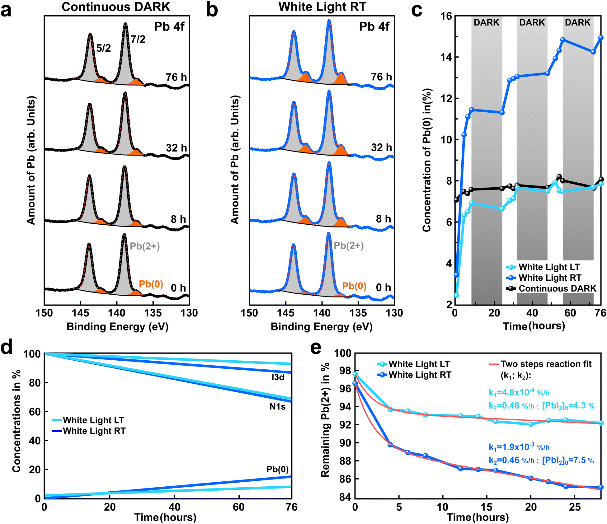 | ||
| Fig. 1 Influence of white light and temperature on the generation of a low degree of oxidation state: Pb(0). (a) and (b) Time evolution of the Pb 4f core-level recorded for (FAPbI3)0.97(MAPbBr3)0.03 perovskite films kept in the dark and exposed to white light, respectively. For better readability, the XPS spectra obtained at distinct times were vertically shifted, while the Pb(0) oxidation state was highlighted in orange. A substantial increase of the Pb(0) signal was observed under white light exposure. (c) Amount of Pb(0) extracted from XPS spectra for the perovskite films kept in the dark (black curve) or exposed to white light but kept at distinct temperatures, either room temperature (blue curve, RT: +30 °C) or low temperature (light-blue curve, LT: −70 °C). The white light was switched ON for 8 hours continuously and then OFF for 16 hours to simulate day and night cycles (highlighted in white/gray, respectively). (d) Evolution of the iodine (two top curves), nitrogen (two middle curves), and Pb(0) content (two bottom curves) for the LT and RT sample depicted in (b) and (c). An increase of Pb(0) is observed with time, light, and temperature. (e) Remaining Pb(2+) vs. time under continuous light exposure for perovskite films kept at RT and LT (blue, and light-blue curves, respectively). The red curves indicate a fit assuming a two steps and first-order chemical reaction: the first step: FAPbI3→PbI2 + FAI; the second step: PbI2→Pb(0) +I2. The speed of the reaction is governed by the limiting reaction, which in our case is the first reaction step (e.g. light generation of PbI2, with k1 as the rate constant). In addition, we assume that PbI2 is continuously transformed into Pb(0), inducing a decay with a k2 rate constant. The fit to the curve is derived from eqn (3). | ||
The ratio of Pb(0) and Pb(2+) oxidation states was also measured at room temperature for a sister FAPI sample exposed to white light for continuous 8 hours followed by 16 h in the dark to mimic day–night cycles. The chemical evolution of the perovskite samples was followed for a total measurement period of 76 h (hereafter labeled as 76 h-light RT), covering a bit more than 3 day/night cycles. In contrast to the sample kept in the dark, a clear increase of the Pb(0) signal was recorded over time for the light-exposed sample (highlighted in orange, Fig. 1b). The X-ray beam power and X-ray time exposure were strictly kept the same for both samples, the only difference comes from the presence or absence of white light. This experiment suggests that white light triggers the formation of metallic lead, as shown by the Pb(0) signal in the XPS spectra (Fig. 1b). The constant amount of Pb(0) recorded for the perovskite sample kept in the dark (Fig. 1a) could be linked to an initial degradation happening before introducing the sample into the XPS vacuum chamber (initial light exposure), or during sample preparation.
The presence of Pb(0) in perovskite film is known to be one of the major bottlenecks that limit a perovskite device's performance and stability. Therefore, it is of great importance to investigate in detail the origin of Pb(0) in perovskite materials and to propose some strategies to mitigate its formation and/or impact. Thereafter, we investigate the impact of the sample temperature on the generation of Pb(0) in FAPI perovskite film. For this purpose we compare the amount of Pb(0) generated over time under white light exposure for two samples, one kept at room temperature (blue curve, Fig. 1c) and one kept at low temperature −70 °C (hereafter: 76 h-light LT, light-blue curve Fig. 1c). As depicted in Fig. 1c, after 76 hours the amount of Pb(0) generated by white light in the perovskite sample kept at room temperature is almost twice as compared to the one for the low-temperature sample (15% instead of 8%), despite comparable Pb(0) before light exposure. This result shows that cooling down the sample reduces Pb(0) generation.
The white and gray shadow overlay in Fig. 1c indicates the 8 h light and 16 h dark conditions that the sample was periodically exposed to in order to simulate day/night cycles. An interesting finding is that the generation of Pb(0) correlates with the days/nights cycles. The generation of metallic lead starts as soon as the white light is switched ON. In contrast, almost no Pb(0) is formed during the night (light is switched OFF). This is even more evident on a sample kept continuously in the dark where the amount of Pb(0) is unchanged during the whole 76 hours experiment (black curve, Fig. 1c). To see this effect better, a comparison of continuous light versus discontinuous light exposure on the generation of Pb(0) is depicted in the ESI† (Fig. S2).
The formation of Pb(0) is accompanied by a loss of iodine and nitrogen (FA molecule), as exemplified in Fig. 1d. The initial and final amounts of iodine, nitrogen, and Pb(0) were determined by XPS for both the 76 h-light RT and LT samples (blue and light-blue curves, respectively). This observation tends to support previous reports in the literature29,32 that suggest the degradation of perovskite is a two steps reaction process, as follows:
 | (1) |
In the first initial step (1), the perovskite material is decomposed into lead iodide and formamidinium iodide. In the present work, we demonstrated that this reaction is triggered by exposure to white light, and not by the X-ray beam (since the power of the X-ray beam is kept low, e.g. low X-ray doses33). This interpretation is supported by earlier reports that have shown tolerance of perovskites against X-rays.34
In the second step (2), the lead iodide with a (2+) oxidation state is transformed into diiodide and metallic lead, leading to the reduction of lead into its 0 oxidation state, as shown by the Pb(0) signal recorded in our XPS measurements.
 | (2) |
For both the LT and RT samples, we have plotted the remaining Pb(2+) versus time for an equivalent of 28 hours of continuous light illumination by omitting the data points acquired during the night cycles (Fig. 1e). To determine the reaction rates of steps (1) and (2), we assumed first-order chemical reactions and then derived an equation for the time evolution of Pb(2+) oxidation state:
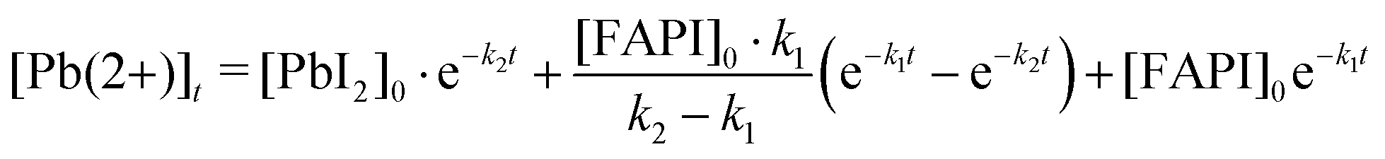 | (3) |
A detailed derivation of eqn (3) is described in the ESI.† The results of the fit are displayed as solid red lines in Fig. 1e. Similar k2 reaction rates are obtained for both the RT and LT light-degraded samples (k2 ≃ 0.5% per h); indicating that temperature does not affect the conversion of PbI2 into Pb(0). In contrast, we found that the k1 reaction rate is reduced by one order of magnitude for the low-temperature sample as compared to the room-temperature sample (Fig. 1e). This suggests that cooling down the sample to −70 °C is preventing reaction (1) from occurring, and that the process is thermally activated, whereas reaction (2) is not thermally activated.
In addition, the high values obtained for k2 as compared to k1 (k2≫100 × k1) showed that reaction (2) is a much faster chemical process than reaction (1), as suggested in earlier reports29,35,36 and as exemplified in Fig. S3 (ESI†). Therefore, we infer that the rapid decay observed during the first 4 hours of light exposure for the LT and RT samples is related to reaction (2) that imposes a quick transformation of the initial PbI2 excess present in the perovskite film as a result of the growth conditions. At room temperature, light triggers new PbI2, while at low temperature this is largely absent.
By comparing these results with the one obtained for the sample kept in the dark, we infer that reactions (1) and (2) are triggered by light. Our two-steps model is able to appropriately describe the time evolution of the Pb(2+) and Pb(0) oxidation states, as depicted in Fig. 1e. However, this model does not fully grasp the time evolution of the volatile FAI and I2 species (see Table S1, ESI†). The discrepancy between the expected amount of I and FA from our model and the higher content measured in the XPS, could be related to ion migrating from the bulk to the surface (XPS probes the topmost 10 nm of the perovskite film). This ion migration might be triggered by the concentration gradient of I and FA at the surface of the perovskite due to light degradation.
2.2 Light-induced topographic and work function changes: AFM, KPFM
To gain further insights into the light-induced degradation of the perovskite surface, we performed atomic force microscopy (AFM) and Kelvin probe force microscopy (KPFM). Fig. 2a–c show the AFM topographic images of a sample kept in the dark (namely control), as well as the 76 h-light degraded LT and RT samples described earlier.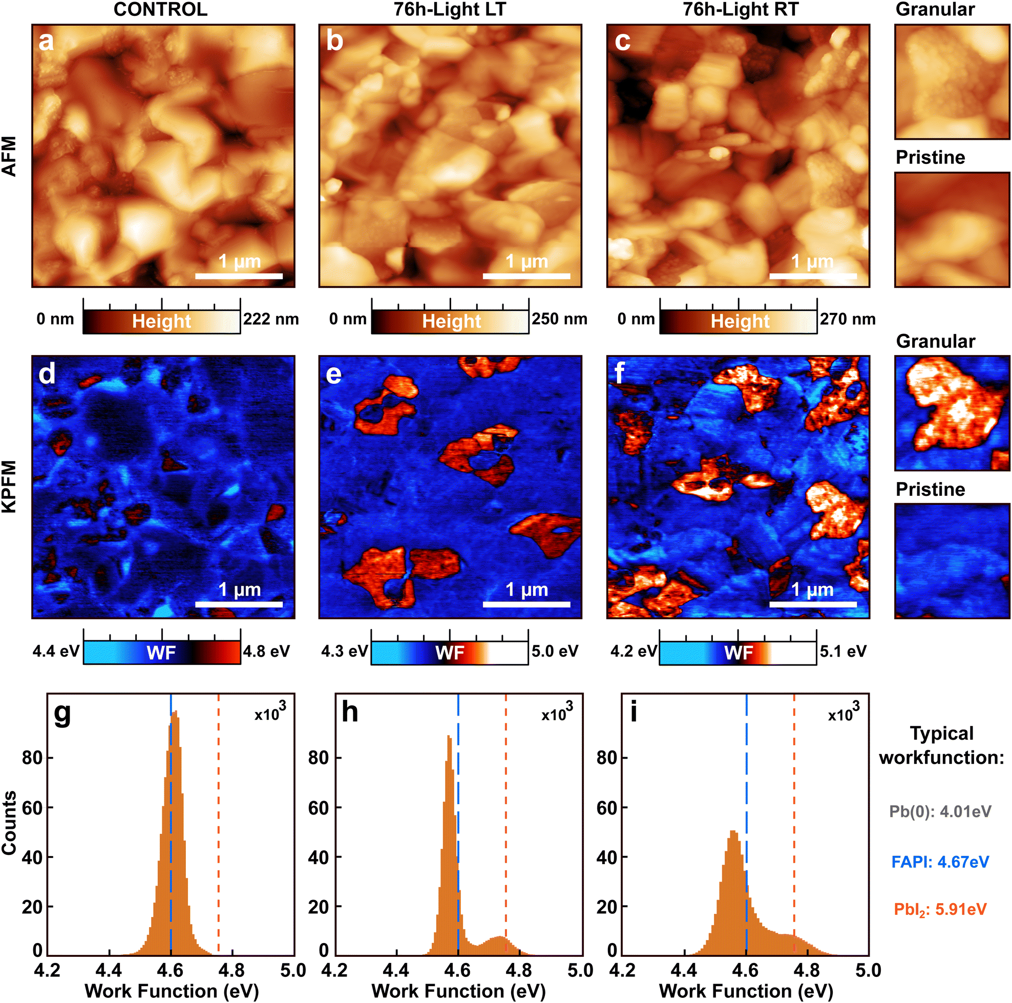 | ||
| Fig. 2 Light-induced topographic and work function modifications. (a)–(c) Topographic images measured by AFM for (FAPbI3)0.97(MAPbBr3)0.03 samples kept respectively in the dark (labeled as control), under white light for 76 h at a temperature of −70 °C (labeled as 76 h-light LT), and under white light for 76 h at room temperature (labeled as: 76 h-light RT). (d)–(f) Work function maps recorded by KPFM on the same areas as the corresponding AFM images in (a)–(c). A higher work function correlates with the presence of granular domains in the topographic image. The images were acquired by using single-pass frequency modulation AFM/KPFM. Insets in c and f depicted the enlarged AFM and KPFM image for pristine and granular domains coexisting at the surface of the 76 h-light RT sample (inset-image size: 800 × 800 nm2). (g)–(i) Histograms of the work function values recorded for the three samples in (d)–(f). Higher and dispersed work function values are observed on the light-degraded samples, as compared to the control. | ||
The morphology of the three samples is composed of smooth and well-oriented grains of an average size of approximately 200 to 250 nm. Some of those grains appear highly textured with additional small granular structures in their interior. Despite those similarities, a relative increase in the amount of the small granular structures is observed for the light-exposed samples with respect to the control sample. This observation is corroborated by an increase in the mean roughness (MR) of the light-exposed samples (MR ≃ 30 nm and MR ≃ 32 nm for LT and RT, respectively) as compared to the control (MR ≃ 29 nm). The 76 h-light RT sample has the highest mean roughness and hosts the highest number of granular structures. We associate those granular structures with the light-induced degradation of the perovskite films.
Work function maps were recorded on the same microscopic areas by KPFM (Fig. 2d–f). In the KPFM maps, blue stands for low work function while red corresponds to higher work function values. Stronger variations were found in the spatial distributions of the work function of light-degraded RT and LT samples, as compared to the control FAPI perovskite film.
The KPFM map of the control sample is uniform with very few domains of high work function. In contrast, the KPFM maps of the 76 h-light degraded LT and RT samples present two distinct phases one with a low work function and one with a higher work function. The KPFM maps depicted in Fig. 2d–f were measured in ultra-high vacuum (UHV) since this method provides higher accuracy on the work function values compared to measurements done under ambient or N2.37 However, recording large-scale images is very demanding in UHV due to the slower scanning speed. Therefore to obtain statistics on the surface coverage of the two work function phases, large-scale KPFM measurements were performed in a N2 environment on a distinct microscope. We estimated that the surface of the control sample is covered by 5.9% of high work function domains, while the 76 h-light LT and RT samples consist of 10.8% and 15.2% of high work function domains, respectively (Fig. S4, ESI†).
Interestingly, we observe a clear correlation between the presence of granular domains in the topographic AFM images and the high work function domains displayed in the KPFM maps. Therefore, those high work function domains must originate from the light-induced degradation process (reaction step (1) or (2)).
The work function changes can be better resolved in the work function distributions of each sample (Fig. 2g–i) extracted from the KPFM maps. Fig. 2g shows that the work function distribution of the control FAPI sample is composed of a single sharp Gaussian peak centered around 4.6 eV (blue dashed line). In contrast, the light-degraded LT and RT samples display two main peaks in their work function distributions centered at 4.55 and 4.75 eV. In addition, a clear broadening is observed for the work function distribution of the 76 h-light RT sample as compared to the LT sample, exemplifying further that cooling down the sample helped reduce the light-degradation process and therefore the appearance of high work function domains at the surface of the perovskite film (reaction step (1)).
From the literature we know the typical work function values that are expected for FAPI perovskite (WF(FAPI) = 4.67 eV), as well as for pure lead (WF(Pb) = 4.01 eV), and PbI2 film (WF(PbI2) = 5.91 eV).38–40 By comparing those tabulated values with the measured work functions at the surface of our FAPI perovskite films, we conclude that the high work function/granular domains might be composed of PbI2 or by a closely related compound with slightly lower work function values such as PbIx, with x < 2. The single Gaussian peak recorded for the control sample at 4.6 eV is very similar to previously reported values for FAPI.38 We attribute the slight downward shift of the main peak of the work function distribution observed for the light-degraded samples with respect to the control (blue dashed line) to the generation of pure metallic lead Pb(0), (reaction step (2)).
2.3 Light-induced chemical composition variations at sub-micrometer-scale: EM, SIMS
To identify the true chemical origin of those high work function/granular domains we performed high-resolution EM and SIMS measurements (Fig. 3) for both a control sample kept in the dark and the 76 h-light RT degraded sample. In agreement with our AFM measurements, the granular domains were found only on the light-degraded sample (Fig. S5, ESI†). In addition, small domains with high brightness contrast are observed in the EM images of both the control and 76 h-light RT samples. It has been shown in previous reports41,42 that the contrast in EM could be affected by the material's work function. Therefore, we attribute these high brightness regions to high work function PbI2 domains. To facilitate the reading of the EM and SIMS data, we have marked with white/yellow contours the high WF domains (PbI2) and granular structures in Fig. 3. The raw EM and SIMS maps without marked regions can be found in the ESI† (Fig. S6).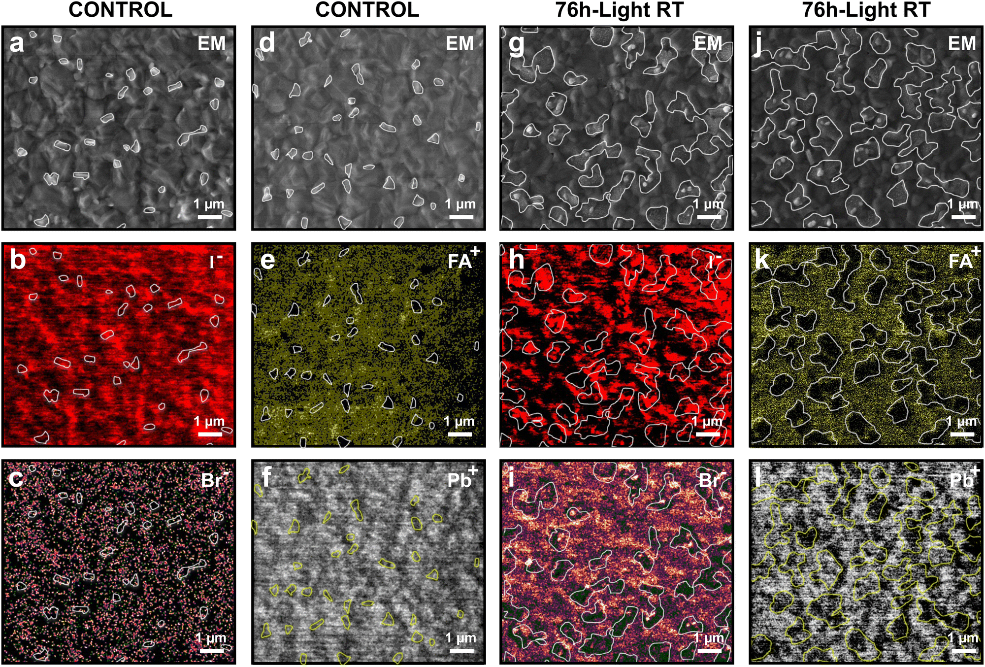 | ||
| Fig. 3 Submicrometric variation of the morphology and chemical composition after light-induced degradation. (a)–(c) EM image of a non-degraded (FAPbI3)0.97(MAPbBr3)0.03 sample kept in the dark (namely, control) and the corresponding SIMS maps for iodine (I−) and bromine (Br−) obtained for negative polarity. (d)–(f) EM image and SIMS maps (FA+ and Pb+) of the same control sample on a different macroscopic location for positive polarity. (g)–(i) EM image of a perovskite sample degraded under white light for 76 hours at room temperature (namely, 76 h-light RT) and the corresponding SIMS maps for iodine (I−) and bromine (Br−). (j)–(l) EM image and SIMS maps (FA+ and Pb+) of the same 76 h-light RT degraded sample on a different macroscopic location. The overlay white/yellow contours correspond to the regions with higher brightness in the EM images (associated with higher work function contrast, due to the presence of PbI2). Correlations can be observed between those regions and a lower amount of organic compounds (FA+), as well as a lower amount of bromine (Br−). | ||
Fig. 3a–f depicts the EM images and the corresponding SIMS maps measured on the control sample for the following ions: iodine (127I−), bromine (79Br−), FA (mass 43, CH3N2), and lead (208Pb+). A first interesting finding is that the high WF domains with high brightness in EM images correspond to regions with low FA and Br contents, supporting our interpretation that those regions are PbI2 domains.
Fig. 3g–l depict the EM and SIMS maps recorded for the 76 h-light RT degraded sample. Surprisingly, the granular structures appear to be all located around high work function PbI2 regions, indicating that the light-degradation is first initiated at those locations (Fig. 3g and j). Therefore, care needs to be taken when designing perovskite films with a PbI2 rich content. PbI2 acts as nucleation points for the light-induced degradation of the material. In addition, the SIMS maps of the 76 h-light RT degraded sample reveal that the granular structures correspond to regions with a reduced amount of FA and Br content (Fig. 3i and k). In contrast, no correlation was found between the granular structure and the Pb or I content (Fig. 3h and l). Therefore, we conclude that the chemical composition of the granular structures is indeed PbIx rich domains (with x < 2), corroborating the high work function measured by KPFM on those domains (Fig. 2).
The SIMS maps for oxygen and C−N organic compound were also measured for both the control and 76 h-light RT degraded sample (Fig. S7, ESI†). After slight exposure to ambient conditions, we observed that the oxygen signal is mainly localized at the position of the PbI2 rich regions of the perovskite. These results further highlight the key role that plays PbI2 domains in the light- and oxygen-degradation of the perovskite film.
The surface chemical modification depicted in Fig. 1–3 would certainly have deleterious effects on a perovskite photovoltaic device's performance and stability. In addition, the presence of I2− vacancies in the granular PbIx defective domains could also contribute to the rapid deterioration of the material by favoring ion motion.
2.4 Energetics of perovskite degradation under light excitation: DFT calculations
To gain some insights on the atomistic origin of the degradation of (FAPbI3)0.97(MAPbBr3)0.03, perovskite we performed Density Functional Theory (DFT) calculations.43,44 We used the generalized gradient approximation (GGA) in the PBE formulation45 capitalizing on the well-known fortuitous error cancellation of spin–orbit coupling (SOC) and many-body effects observed in 3D lead halide perovskites.46 However, we also conducted additional calculations employing PBE0 exchange–correlation functional47 augmented with long-range van der Waals (vdW) corrections based on the many body dispersion (MBD) NL48 method including SOC, known for its higher level of accuracy. Due to the substantial computational cost, we were unable to exclusively rely on the latter protocol for all calculations. Consequently, we present results from both methods, demonstrating that qualitatively, the outcomes align using both protocols. In our theoretical approach, we focus on pure FAPbI3, a choice that can be justified by the small percentage of MAPbBr3. To simulate the effect of light, we performed calculations where we introduced either an extra hole or an extra electron. This approach has already been employed on pristine MAPbI3 perovskite and has shown great potential to predict the impact of light exposure on material properties.49 Initially, we aimed at identifying if the degradation of FAPbI3 is more probable in the ground state or while a charge is introduced to simulate excited states. Hence, we calculated the dissociation enthalpy (DE) of FAPbI3 with respect to the precursor phases (PbI2 and FAI) considering both the pristine and charged systems. Reaction (4) represents the ground state while reactions (5) and (6) correspond to charged states (e.g. excited states). The dissociation enthalpy for FAPbI3 is defined in (7).| FAPbI3 → PbI2 + FAI | (4) |
| FAPbI3+→PbI2+ + FAI | (5) |
| FAPbI3−→PbI2− + FAI | (6) |
| DE(FAPbI3) = E(PbI2) + E(FAI) − E(FAPbI3) | (7) |
Several types of defects have been reported so far, some of them have a detrimental impact on the power conversion efficiency and stability of halide perovskites. For example, a Vk center is a defect in which a hole is shared by two neighboring halogen ions, I2−. This defect is formed of a metal bringing I2− dimer upon the trapping of a hole.50 The formation of a Vk center does not involve adding an additional ion or creating a vacancy. In a similar spirit, an H center is a defect that is formed by the interaction of an interstitial ion and a lattice halide ion.51 In addition, the formation of interstitial iodine accompanied by a vacancy-site defect under hole-rich conditions is called an iodine Frenkel defect.52 By vacancy, we refer to the case where an ion is not present at its lattice site.
Aiming at studying the formation of I2− dimer as a potential mechanism for the degradation of FAPbI3, we focus on the thermodynamics of hole trapping through the formation of Vk center defects. We perform two types of calculations. First, we initially introduce an extra hole and relax the structure. Secondly, we also move two iodine atoms close to each other at a distance of 3.2 Å, (an equilibrium distance of I2− dimer) creating a Vk center and relaxing the structure in the presence of an extra hole while constraining the distance between the two iodine ions during the calculation. For the former, the hole is found to be delocalized over the whole perovskite crystal structure (Fig. 4a). However, for the latter, the extra hole is localized on the dimer thus favoring hole trapping (Fig. 4b). We then calculated the I–I defect formation energy which is 0.25 eV, thus indicating that the dimer formation is disfavored.
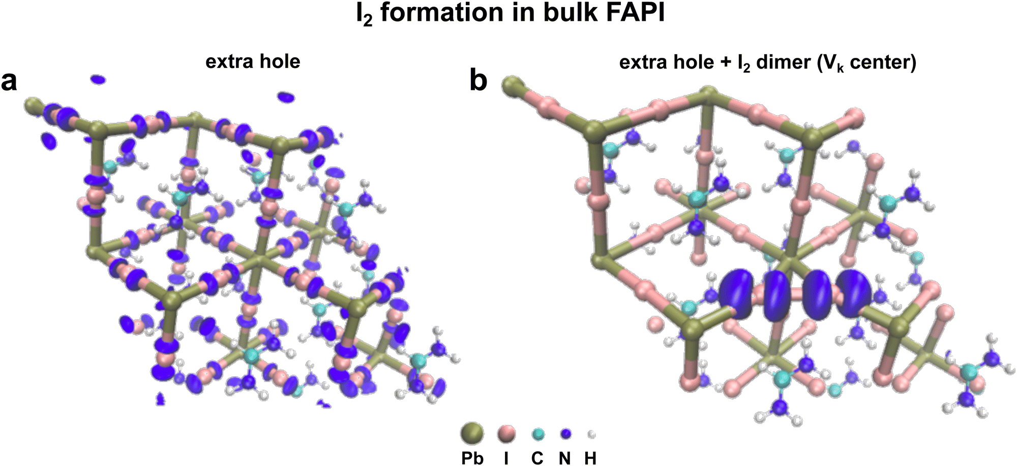 | ||
| Fig. 4 Charge densities representing the valence band maximum (VBM) of bulk FAPbI3. (a) Charge density in the presence of an extra hole while no defect has been introduced in the structure. The charge density is delocalized. (b) Charge density in the presence of an extra hole and a Vk center. The Vk defect center was formed by moving two iodine ions close to each other. The distance separating the two iodine ions is kept constant during the calculation. The charge density is localized on the area of the defect. | ||
This phenomenon described here has also been reported for bulk MAPbI3.49 Here, from our calculations, we show that hole-trapping as well as I2− dimer defects are unlikely to be formed spontaneously. However, if the Vk center defect has already been created, then the hole can localize on it. A similar analysis has been performed in the case of PbI2 (ESI,† Fig. S8). Spontaneous hole-trapping has not been observed, but I2− dimer would trap a hole if it is already present in the system. Several reports in the literature suggested that perovskite instantaneous device efficiency is barely affected by the presence of defects,53–55 however, our experimental results as well as our DFT calculations suggest that defects such as Vk centers (I2− dimer), play a key role in the long-term degradation mechanism of perovskite absorbers under light exposure (e.g. with extra hole). In fact, the light-induced chemical degradation processes of perovskite appear to be rather a defect-intolerant phenomenon. From our outcomes, it is evident that the presence of defects such as I2− dimers will trigger perovskite degradation once the material is exposed to light. We infer that those I2− dimers are more likely to appear in defective PbIx granular structures (as the one seen in the experiment), where the perovskite crystal structure might undergo slight deformation due to the strain imposed by the iodine vacancies. Therefore the generation of PbIx granular structures might promote perovskite degradation under light exposure by facilitating the formation of Vk center defects.
2.5 Light-induced bandgap variations at the nanometer-scale: STM, STS
To further study the impact of PbIx (x < 2), and PbI2 domains on the electronic properties of the perovskite film, we performed scanning tunneling microscopy and spectroscopy (STM, STS) on the 76 h-light RT degraded sample (Fig. 5). STS allows for the determination of the local density of states of the sample with nanometer-scale lateral resolution. This is achieved by sweeping the voltage applied in the tunneling junction meanwhile recording its conductance characteristic (I/V). For semiconductors, this allows for evaluating the positions of the valence and conduction bands onsets (VB, CB) by recording electron transfer from/to the filled/empty states near the Fermi level.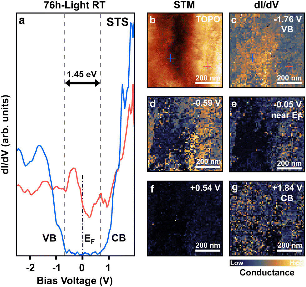 | ||
| Fig. 5 Bandgap variation at the nanoscale on pristine and light-degraded perovskite domains. (a) Scanning tunneling spectroscopy (STS) recorded on pristine (blue curve) and granular (red curve) domains as indicated with blue/red crosses in the topographic image and dI/dV maps, in b and c respectively. Both domains are present at the surface of the 76 h-light RT degraded (FAPbI3)0.97(MAPbBr3)0.03 perovskite film. (b) Topographic STM image of the 76 h-light RT degraded sample. (c)–(g) Corresponding dI/dV (conductance) maps recorded at distinct sample voltages (energies). Typical lock-in parameters are as follows: Vmod = 20 mV; frequency = 965 Hz; sensitivity = 500 mV; and time constant = 10 ms. Tunneling parameters are It = 0.1 nA; bias = −1.5 V. Conductance maps are depicted in arbitrary units. The scale bar indicates the color code for low and high conductance. | ||
To improve the signal-to-noise ratio, the lock-in detection technique was employed which allows a direct measurement of the sample's local density of state by recording the derivative of the conductance (dI/dV). Fig. 5a, shows the STS spectra obtained for the 76 h-light RT degraded sample. The blue and red curves correspond to the spectra recorded at the location marked with blue/red crosses in the topographic STM image in b. Stringent differences in electronic behavior can be noticed between these two sample locations. The spectra taken at the position of the blue cross present typical VB and CB onsets separated by a 1.45 eV bandgap, as is expected for a semiconductor material such as FAPI56 perovskite (Fig. 5a). Therefore, we attribute this characteristic to non-degraded FAPI perovskite.
In contrast, the spectra recorded at the red-cross location presents a completely different behavior, with a non-zero conductance signal that crosses the Fermi level before a sudden drop. This behavior is expected for metallic materials, and we associate it with light-induced metallic lead Pb(0) embedded in PbIx granular domains. This I/V characteristic is correlated to the granular-like appearance of the domain where the red spectrum was measured.
Conductance maps (dI/dV) recorded on the same area as the topographic image in b are depicted in Fig. 5c–g, for distinct bias voltage (e.g. energies). The dI/dV map at −1.76 V shows a higher conductance on the domain on the left of Fig. 5c which corresponds to electron transfer from the VB of the non-degraded FAPI perovskite domain towards the probe tip. However, almost no conductance is measured on the right granular domain (light-degraded area).
Inversely, at low bias voltage (Fig. 5d and e) near the Fermi level, the conductance is higher on the granular light-degraded domains due to its metallic behavior, while no conductance is observed in the pristine FAPI domain. Those modifications of the surface electronic properties can be observed over well-defined domains of about 200 to 300 nm in size. Similar electronic behaviors were observed for the 76 h-light LT degraded sample (Fig. S9, ESI†).
Local bandgap variations are detrimental to device performance. The presence of metallic domains with no bandgap will undoubtedly impact the charge extraction at the perovskite interface. In addition, compositional changes at the perovskite surface have been shown to strongly modify the interaction at the interface between the perovskite and charge transport layer.57 Preventing the light-induced conversion of FAPI into PbI2 and PbIx granular structures is a must to obtain high performance and long-term stability in perovskite solar cells.
2.6 Beneficial effect of passivation and wavelength selective filters on perovskite stability against light
Thereafter, we investigate the impact of surface passivation and wavelength selective filters on the perovskite stability under light excitation (Fig. 6). First, the effect of surface passivation was determined by tracking the time evolution of the Pb(0) signal in XPS for a (FAPbI3)0.97(MAPbBr3)0.03 perovskite film treated with an organic biphenyl-4,4-dithiol layer (labeled as Pa). Fig. 6a, presents a comparison of the amount of light-generated Pb(0) with and without the Pa passivation layer (blue vs. purple curve). The XPS results show a clear reduction of the Pb(0) signal after 76 h of light exposure for the passivated sample (8.5%) as compared to the pristine perovskite film (15%). In particular, during the first initial 8 h of light exposure, the amount of Pb(0) generated is reduced by half, demonstrating a much higher stability of the passivated perovskite samples.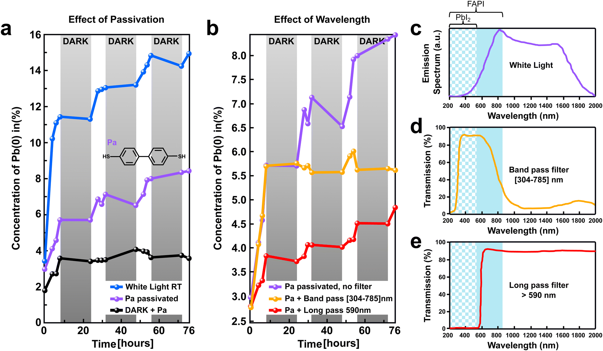 | ||
| Fig. 6 Effect of passivation and wavelength selective filters on perovskite stability against light. (a) Time evolution of the Pb(0) signal obtained on unpassivated (FAPbI3)0.97(MAPbBr3)0.03 perovskite (blue curve) and passivated perovskite film with a Pa organic layer (purple curve). Both samples were periodically exposed to white light to simulate day and night cycles (highlighted with white and gray background). The black curve corresponds to the Pb(0) time evolution recorded on a passivated perovskite film kept continuously in the dark. Inset: The chemical structure of the Pa organic molecule used for passivation. (b) Time evolution of the Pb(0) signal obtained on passivated (FAPbI3)0.97(MAPbBr3)0.03 perovskite films with a band pass filter (304 ≤ λ ≤ 785 nm, orange curve); with long pass filter (λ ≥ 590 nm, red curve); and without filter (purple curve, same as in (a)). (c) Schematic representation of the emission spectrum of the white light used for excitation. The absorption range of FAPI perovskite and PbI2 are highlighted with a blue solid and chessboard background, respectively. (d) and (e) Transmission spectra of the band pass and long pass filters used in b. The bandpass filter allows absorption of light by both FAPI and PbI2 domains, while it is blocking the infrared light. In contrast, the long pass filter allows absorption only by the FAPI domains, while the whole sample is irradiated by infrared light. | ||
In addition, we found that the stability of the perovskite film could be further improved by using wavelength-selective filters by allowing only a specific energy range of the light to reach the sample. Fig. 6b, depicted the light-generated Pb(0) signal as a function of time for Pa-passivated perovskite films without (purple curve) and with wavelength selective filters (orange and red curves). Substantial reduction of Pb(0) signal was observed for the perovskite film exposed to filtered light as compared to non-filtered white light with a broad emission spectrum (Fig. 6b). The reduction of the Pb(0) signal for the samples exposed to filtered light is corroborated with a decrease in the losses of iodine and FA (Table S2, ESI†).
To better understand the origin of the increased stability recorded for the perovskite film exposed to filtered light, it is important to look at the specifications of the light source and wavelength selective filters used (Fig. 6c–e). The white light source used has a broad emission spectrum between 400 to 2000 nm wavelengths (Fig. 6c) with an irradiance of 16 mW cm−2, e.g. 0.16 sun equivalent. It is important to notice that our perovskite films have a 1.45 eV bandgap, which means that they absorb light with wavelengths of 856 nm and below (highlighted with a blue background, λ ≤ 856 nm). Two types of filters were used, a bandpass and a long pass filter. The bandpass filter allows transmission of the light with a specific wavelength within the range 304 ≤ λ ≤ 785 nm, as depicted in Fig. 6d. This range corresponds to light that can be absorbed by both the FAPI and PbI2 domains, as highlighted by the blue solid and chessboard background in Fig. 6d. Importantly, our bandpass filters do not allow light in the infrared region to irradiate the perovskite film. In contrast, the long pass filter used allows for transmission of light with a wavelength above 590 nm (λ ≥ 590 nm). This corresponds to the light that can be absorbed by the FAPI domains only (solid blue background, Fig. 6e). Moreover, the infrared light is allowed to irradiate the perovskite film by our long-pass filter.
A similar Pb(0) increase was observed during the first 8 h for both the samples without filter and with band pass filter (purple and orange curve, Fig. 6b). As demonstrated earlier, the rapid initial increase of Pb(0) recorded during the first 8 hours of light exposure is mainly governed by the conversion of PbI2 excess (from the growth conditions) into metallic lead. Therefore, we infer that allowing the light with wavelengths in the absorption range of PbI2 domains to irradiate the sample (λ ≤ 515 nm) promotes a faster conversion of PbI2 into metallic lead. In contrast, preventing the light with a wavelength in the absorption range of PbI2 domains to reach the sample, allows for a substantial reduction of the initial increase of Pb(0) during the first 8 h (e.g. slow down the PbI2 → Pb(0) + I2 reaction), as exemplified for the perovskite film with a long pass filter (red curve, Fig. 6b).
Interestingly, for the sample with a bandpass filter, after the first initial increase, we observe stabilization of the Pb(0) amount around a plateau at 6%. In contrast, for the sample without a filter as well as for the sample with a long-pass filter, a slow but steady increase of the Pb(0) amount is observed between 8 h and 76 h (purple and red curves, Fig. 6b). Because the bandpass filter does not allow the infrared light to penetrate the perovskite film while both the long pass filter and the white light does, we infer that the infrared light is responsible for the slow increase of Pb(0) recorded between 8 h and 76 h.
These findings could have substantial implications for the long-term stability of the perovskite film. For stable perovskite film, we propose that PbI2 excess must be avoided to prevent the initial degradation of the material. In addition, bandpass filters should be used to protect the perovskite film from infrared light in order to improve long-term stability.
3 Conclusions
In this study, we employed multiscale characterization tools to investigate the impact of light on the chemical degradation of state-of-the-art (FAPbI3)0.97(MAPbBr3)0.03 perovskite film. By XPS, SIMS, and EM we demonstrated that white light triggers the generation of metallic lead (Pb (0)) and defective PbIx granular domains at the perovskite surface. KPFM and STM showed that these degraded areas have higher work function and metallic I–V characteristics which are detrimental to the long-term performance of perovskite devices. Our DFT calculations suggest that Vk center defects, as expected in perovskites with PbIx and PbI2-rich domains, would promote light-induced degradation of perovskite absorbers. We employed an organic molecule for surface passivation which slows down the degradation. Furthermore, we demonstrated that light degradation is a wavelength-dependent phenomenon in perovskite material. We employed dedicated bandpass and long-pass filters that enabled us to reduce by half the amount of metallic lead generated under light exposure. Overall, our results show that light-induced degradation is a both defect-assisted and light wavelength-dependent phenomenon. Based on the outcome of these findings, we can develop innovative strategies to mitigate light-induced degradation of perovskite film. In particular, bandpass, and long-pass filters could be employed for filtering out the detrimental infrared radiation that triggers the long-term degradation of the perovskite material. In addition, the use of perovskite films with a high density of defects and with PbI2-rich domains should be avoided since they can act as seeds for light-induced degradation. Finally, our results reveal that special care needs to be taken when analyzing the stability of fully processed perovskite solar cells. According to our nanoscale analysis, the amount of infrared light in the solar spectrum will greatly change the long-term stability of the perovskite device. This can be traced back to the intrinsic stability of the perovskite layer, but also to the stability of the extraction layers, which may be damaged/modified at different rates because of varying amounts of iodine and organic fragments that leave the perovskite. Future studies need to focus on pinpointing the exact wavelength that promotes decomposition to filter out this contribution. This will be especially important for tandem applications, where the amount of infrared light passing through the perovskite top cell is often maximized. Our results show that this may lead to a reduction in long-term stability.Author contributions
J. H. performed the XPS, AFM/KPFM, and STM/STS measurements in an ultra-high vacuum. A. B. performed the DFT calculations with the help and supervision of A. T.; the growth and optimization of the (FAPbI3)0.97(MAPbBr3)0.03 perovskite films were made by A. K., while J. F. M. grew the PbI2 films. J.-N. A. performed the EM and SIMS measurements. M. U. F. carried out the wide range AFM/KPFM measurements in a N2 environment. A. R. conceptualized the experiments, and supervised the project. All authors participated in the data analysis and in the manuscript writing.Conflicts of interest
There are no conflicts to declare.Acknowledgements
This research was funded by the Luxembourg National Research Fund (FNR), grant references [11244141,11696002,12246511,13390539,14735144,14757355]. In addition, funding within the DFG priority program SPP 2196 is acknowledged. A. K. acknowledges funding from the European Unions Horizon 2020 Research and Innovation program under the Marie Skłodowska-Curie Grant Agreement No. 843453. A. B. and A. K. thank the HPC platform of the University of Luxembourg for computer resources.References
- National Renewable Energy Laboratory NREL Chart, https://www.nrel.gov/pv/cell-efficiency.html, 2023.
- M. A. Green, E. D. Dunlop, G. Siefer, M. Yoshita, N. Kopidakis, K. Bothe and X. Hao, Prog. Photovoltaics, 2023, 31, 3–16 Search PubMed.
- P. Wang, Y. Wu, B. Cai, Q. Ma, X. Zheng and W.-H. Zhang, Adv. Funct. Mater., 2019, 29, 1807661 CrossRef CAS.
- C. Stecker, K. Liu, J. Hieulle, R. Ohmann, Z. Liu, L. K. Ono, G. Wang and Y. Qi, ACS Nano, 2019, 13, 12127–12136 CrossRef CAS PubMed.
- A. Jamshaid, Z. Guo, J. Hieulle, C. Stecker, R. Ohmann, L. K. Ono, L. Qiu, G. Tong, W. Yin and Y. Qi, Energy Environ. Sci., 2021, 14, 4541 RSC.
- X. Xiao, J. Dai, Y. Fang, J. Zhao, X. Zheng, S. Tang, P. N. Rudd, X. C. Zeng and J. Huang, ACS Energy Lett., 2018, 3, 684–688 CrossRef CAS.
- B. Rivkin, P. Fassl, Q. Sun, A. D. Taylor, Z. Chen and Y. Vaynzof, ACS Omega, 2018, 3, 10042–10047 CrossRef CAS PubMed.
- D. Wei, F. Ma, R. Wang, S. Dou, P. Cui, H. Huang, J. Ji, E. Jia, X. Jia, S. Sajid, A. M. Elseman, L. Chu, Y. Li, B. Jiang, J. Qiao, Y. Yuan and M. Li, Adv. Mater., 2018, 30, 1707583 CrossRef PubMed.
- Y. Lin, Y. Bai, Y. Fang, Q. Wang, Y. Deng and J. Huang, ACS Energy Lett., 2017, 2, 1571–1572 CrossRef CAS.
- H. Yuan, E. Debroye, K. Janssen, H. Naiki, C. Steuwe, G. Lu, M. Moris, E. Orgiu, H. Uji-i, F. D. Schryver, P. Samorì, J. Hofkens and M. Roeffaers, J. Phys. Chem. Lett., 2016, 7, 561–566 CrossRef CAS PubMed.
- J. S. Yun, J. Seidel, J. Kim, A. M. Soufiani, S. Huang, J. Lau, N. J. Jeon, S. I. Seok, M. A. Green and A. Ho-Baillie, Adv. Energy Mater., 2016, 6, 1600330 CrossRef.
- Y. Shao, Y. Fang, T. Li, Q. Wang, Q. Dong, Y. Deng, Y. Yuan, H. Wei, M. Wang, A. Gruverman, J. Shield and J. Huang, Energy Environ. Sci., 2016, 9, 1752–1759 RSC.
- B. Chen, M. Yang, X. Zheng, C. Wu, W. Li, Y. Yan, J. Bisquert, G. Garcia-Belmonte, K. Zhu and S. Priya, J. Phys. Chem. Lett., 2015, 6, 4693–4700 CrossRef CAS PubMed.
- S. G. Motti, J. B. Patel, R. D. Oliver, H. J. Snaith, M. B. Johnston and L. M. Herz, Nat. Commun., 2021, 12, 1–9 CrossRef PubMed.
- P. V. Kamat and M. Kuno, Acc. Chem. Res., 2021, 54, 520–531 CrossRef CAS PubMed.
- D. Lan, Prog. Photovoltaics Res. Appl., 2020, 28, 533–537 CrossRef CAS.
- W. Zhou, J. Gu, Z. Yang, M. Wang and Q. Zhao, J. Phys. D: Appl. Phys., 2020, 54, 063001 CrossRef.
- T. Zhang, C. Hu and S. Yang, Small Methods, 2020, 4, 1900552 CrossRef CAS.
- S. Kim, S. Bae, S.-W. Lee, K. Cho, K. D. Lee, H. Kim, S. Park, G. Kwon, S.-W. Ahn, H.-M. Lee, Y. Kang, H.-S. Lee and D. Kim, Sci. Rep., 2017, 7, 1–5 CrossRef PubMed.
- M. Miyazaki, Y. Sugawara and Y. J. Li, Beilstein J. Nanotechnol., 2022, 13, 712–720 CrossRef CAS PubMed.
- S. Wieghold, E. M. Cope, G. Moller, N. Shirato, B. Guzelturk, V. Rose and L. Nienhaus, ACS Energy Lett., 2022, 2211–2218 CrossRef CAS.
- S. Wieghold, N. Shirato and V. Rose, J. Appl. Phys., 2020, 128, 125303 CrossRef CAS.
- H.-C. Hsu, B.-C. Huang, S.-C. Chin, C.-R. Hsing, D.-L. Nguyen, M. Schnedler, R. Sankar, R. E. Dunin-Borkowski, C.-M. Wei, C.-W. Chen, P. Ebert and Y.-P. Chiu, ACS Nano, 2019, 13, 4402–4409 CrossRef CAS PubMed.
- M. C. Shih, S. S. Li, C. H. Hsieh, Y. C. Wang, H. D. Yang, Y. P. Chiu, C. S. Chang and C. W. Chen, Nano Lett., 2017, 17, 1154–1160 CrossRef CAS PubMed.
- S. Svanström, A. G. Fernández, T. Sloboda, T. J. Jacobsson, H. Rensmo and U. B. Cappel, Phys. Chem. Chem. Phys., 2021, 23, 12479–12489 RSC.
- W. C. Lin, W. C. Lo, J. X. Li, Y. K. Wang, J. F. Tang and Z. Y. Fong, npj Mater. Degrad., 2021, 5, 1–6 CrossRef.
- M. E. Stuckelberger, T. Nietzold, B. M. West, Y. Luo, X. Li, J. Werner, B. Niesen, C. Ballif, V. Rose, D. P. Fenning and M. I. Bertoni, J. Phys. Chem. C, 2020, 124, 17949–17956 CrossRef CAS.
- K. Motoki, Y. Miyazawa, D. Kobayashi, M. Ikegami, T. Miyasaka, T. Yamamoto and K. Hirose, J. Appl. Phys., 2017, 121, 085501 CrossRef.
- E. J. Juarez-Perez, L. K. Ono, M. Maeda, Y. Jiang, Z. Hawash and Y. Qi, J. Mater. Chem. A, 2018, 6, 9604–9612 RSC.
- J. Hieulle, X. Wang, C. Stecker, D.-Y. Son, L. Qiu, R. Ohmann, L. K. Ono, A. Mugarza, Y. Yan and Y. Qi, J. Am. Chem. Soc., 2019, 141, 3515–3523 CrossRef CAS PubMed.
- J. Hieulle, S. Luo, D. Y. Son, A. Jamshaid, C. Stecker, Z. Liu, G. Na, D. Yang, R. Ohmann, L. K. Ono, L. Zhang and Y. Qi, J. Phys. Chem. Lett., 2020, 11, 818–823 CrossRef CAS PubMed.
- P. Gratia, G. Grancini, J.-N. Audinot, X. Jeanbourquin, E. Mosconi, I. Zimmermann, D. Dowsett, Y. Lee, M. Grätzel, F. De Angelis, K. Sivula, T. Wirtz and M. K. Nazeeruddin, J. Am. Chem. Soc., 2016, 138, 15821–15824 CrossRef CAS PubMed.
- L. Pan, S. Shrestha, N. Taylor, W. Nie and L. R. Cao, Nat. Commun., 2021, 12, 1–9 CrossRef PubMed.
- A. R. Kirmani, A. E. Mansour, C. Yang, R. Munir, A. M. El-Zohry, O. F. Mohammed and A. Amassian, PLoS One, 2020, 15, 1–16 CrossRef PubMed.
- B. Roose, K. Dey, Y. H. Chiang, R. H. Friend and S. D. Stranks, J. Phys. Chem. Lett., 2020, 11, 6505–6512 CrossRef CAS PubMed.
- G. Tumen-Ulzii, C. Qin, D. Klotz, M. R. Leyden, P. Wang, M. Auffray, T. Fujihara, T. Matsushima, J. W. Lee, S. J. Lee, Y. Yang and C. Adachi, Adv. Mater., 2020, 32, 1–7 CrossRef PubMed.
- E. M. Lanzoni, T. Gallet, C. Spindler, O. Ramírez, C. K. Boumenou, S. Siebentritt and A. Redinger, Nano Energy, 2021, 88, 106270 CrossRef CAS.
- C. Ma, B. Kim, D. H. Kang, S. W. Kim and N. G. Park, ACS Energy Lett., 2021, 6, 2817–2824 CrossRef CAS.
- P. A. Anderson and A. L. Hunt, Phys. Rev., 1956, 102, 367–368 CrossRef CAS.
- H. Chen, H. Yan and Y. Cai, Chem. Mater., 2022, 34, 1020–1029 CrossRef CAS.
- J. Cazaux, Ultramicroscopy, 2010, 110, 242–253 CrossRef CAS PubMed.
- Y. Zhou, D. S. Fox, P. Maguire, R. O'Connell, R. Masters, C. Rodenburg, H. Wu, M. Dapor, Y. Chen and H. Zhang, Sci. Rep., 2016, 6, 1–8 CrossRef PubMed.
- P. Hohenberg and W. Kohn, Phys. Rev., 1964, 136, B864–B871 CrossRef.
- W. Kohn and L. J. Sham, Phys. Rev., 1965, 140, A1133–A1138 CrossRef.
- J. P. Perdew, K. Burke and Y. Wang, Phys. Rev. B: Condens. Matter Mater. Phys., 1996, 54, 16533–16539 CrossRef CAS PubMed.
- J. Even, L. Pedesseau, J.-M. Jancu and C. Katan, J. Phys. Chem. Lett., 2013, 4, 2999–3005 CrossRef CAS.
- J. P. Perdew, M. Ernzerhof and K. Burke, J. Chem. Phys., 1996, 105, 9982–9985 CrossRef CAS.
- J. Hermann and A. Tkatchenko, Phys. Rev. Lett., 2020, 124, 146401 CrossRef CAS PubMed.
- F. Ambrosio, E. Mosconi, A. A. Alasmari, F. A. S. Alasmary, D. Meggiolaro and F. D. Angelis, Chem. Mater., 2020, 32, 6916–6924 CrossRef CAS.
- A. Popov, E. Kotomin and J. Maier, Solid State Ionics, 2017, 302, 3–6 CrossRef CAS.
- R. Williams and K. Song, J. Phys. Chem. Solids, 1990, 51, 679–716 CrossRef CAS.
- S. H. Kim and D. Lee, J. Phys. Chem. C, 2019, 123, 9629–9633 CrossRef CAS.
- J. Kang and L.-W. Wang, J. Phys. Chem. Lett., 2017, 8, 489–493 CrossRef CAS PubMed.
- H. Huang, M. I. Bodnarchuk, S. V. Kershaw, M. V. Kovalenko and A. L. Rogach, ACS Energy Lett., 2017, 2, 2071–2083 CrossRef CAS PubMed.
- I. du Fossé, J. T. Mulder, G. Almeida, A. G. M. Spruit, I. Infante, F. C. Grozema and A. J. Houtepen, J. Am. Chem. Soc., 2022, 144, 11059–11063 CrossRef PubMed.
- F. F. Targhi, Y. S. Jalili and F. Kanjouri, Results Phys., 2018, 10, 616–627 CrossRef.
- C. Stecker, Z. Liu, J. Hieulle, S. Zhang, L. K. Ono, G. Wang and Y. Qi, ACS Nano, 2021, 15, 14813–14821 CrossRef CAS PubMed.
Footnote |
| † Electronic supplementary information (ESI) available. See DOI: https://doi.org/10.1039/d3ee03511e |
| This journal is © The Royal Society of Chemistry 2024 |