
Triboelectric junction: a model for dynamic metal–semiconductor contacts†
Xiaote
Xu
 ab,
Zhong Lin
Wang
*cd and
Zhengbao
Yang
*ab
ab,
Zhong Lin
Wang
*cd and
Zhengbao
Yang
*ab
aDepartment of Mechanical and Aerospace Engineering, Hong Kong University of Science and Technology, Clear Water Bay, Hong Kong, China. E-mail: zbyang@ust.hk
bDepartment of Mechanical Engineering, City University of Hong Kong, Hong Kong, China
cBeijing Institute of Nanoenergy and Nanosystems, Chinese Academy of Sciences, Beijing, 101400, People's Republic of China. E-mail: zhong.wang@mse.gatech.edu
dSchool of Materials Science and Engineering, Georgia Institute of Technology, Atlanta, GA 30332, USA
First published on 15th November 2023
Abstract
Static metal–semiconductor contacts are classified into Ohmic contacts and Schottky contacts. As for dynamic metal–semiconductor contacts, the in-depth mechanism remains to be studied. We here define a “triboelectric junction” model for analyzing dynamic metal–semiconductor contacts, where a space charge region induced by the triboelectric effect dominates the electron–hole separation process. Through theoretical analysis and experiments, we conclude that the triboelectric junction influences the electric output in two aspects: (1) the junction direction determines the output polarity; (2) the junction strength determines the output magnitude. Both the junction direction and junction strength are closely related to the electron-affinity difference between the contact metal and semiconductor.
Broader contextHarnessing green energy is an effective solution for addressing the energy crisis. Semiconductor materials have played a significant role in advancing green energy, exemplified by the well-established photovoltaic effect and the emerging tribovoltaic effect. Solar cells, renowned for their remarkable commercial success in the energy sector, employ semiconductors to efficiently convert solar energy into electrical energy through the photovoltaic effect. Similarly, dynamic semiconductor generators harvest mechanical energy through the tribovoltaic effect. However, further investigation is needed to understand the underlying mechanism of the tribovoltaic effect. While many studies have explained this effect based on static junction theories like Schottky junction and PN junction, the effect of triboelectric charge at the contact interface calls for further investigation. To address this issue, we have defined a novel “triboelectric junction” model specifically for analyzing dynamic metal–semiconductor contacts. This work provides a fresh perspective on the mechanism of dynamic metal–semiconductor contacts, paving the way for further fundamental discoveries and potential applications. |
Introduction
Metal–semiconductor contacts, including Ohmic contacts and Schottky contacts, are fundamental for modern electronics.1 Ohmic contacts exhibit linear current–voltage curves, presenting non-rectifying characteristics. Ohmic contacts are usually desirable for effective charge conduction between semiconductors and external circuitry, such as source/drain–semiconductor contacts in transistors.2,3 On the other hand, Schottky contacts form Schottky barriers at metal–semiconductor interfaces, demonstrating rectifying characteristics.4 Schottky contacts find applications in various scenarios, such as rectification in diodes5 and electron–hole separation in solar cells.6 Overall, metal–semiconductor contacts significantly contribute to the advancement of both the electronic and energy industries.The classical metal–semiconductor contacts discussed above are static contacts. Recently, dynamic metal–semiconductor contacts have started to gain attention in the energy-harvesting field.7–11 However, dark clouds are hanging over the mechanism of dynamic metal–semiconductor contacts.12,13 Schottky junction theory, established for static contacts, is widely adopted for explaining dynamic metal–semiconductor contacts.12,13 However, some specific output characteristics cannot be sufficiently explained by the Schottky junction theory (see Fig. S1e and f, ESI†). These discrepancies suggest that the influence of the triboelectric charge at the contact interface must be further investigated. Previous studies have also demonstrated that the interfacial triboelectric field dominates the electron–hole separation process in dynamic semiconductor–semiconductor contacts.14–16 In classical semiconductor physics, surface states are important factors in analyzing contact issues,17 not to mention the unavoidable triboelectric charge induced by dynamic contacts. Thus, there is a necessity for a novel model that considers the influence of the triboelectric charge to better interpret dynamic metal–semiconductor contacts.
Herein, we define a novel “triboelectric junction” model to analyze the in-depth mechanism of dynamic metal–semiconductor contacts. We demonstrate that the triboelectric junction dominates the electron–hole separation process in dynamic contacts. We present a theoretical analysis of the triboelectric junction, elucidating the electric field and electric potential distributions. We develop a material's figure-of-merit, based on the electron-affinity difference, to characterize both the output polarity and magnitude. This work provides a new perspective on the mechanism of dynamic metal–semiconductor contacts, which opens up avenues for further fundamental discoveries and potential applications.
Results
Theory of the triboelectric junction
Let's start by learning about the photovoltaic effect, which involves the use of semiconductors to convert solar energy into electricity. As a mature technology, solar cells operate based on a well-established working mechanism.1,18 This mechanism can be interpreted through the following steps (see Fig. 1a): (1) a PN junction or Schottky junction occurs at the contact interface due to the alignment of Fermi levels; (2) non-equilibrium electron–hole generation is induced by incident photons with energy exceeding the semiconductor bandgap; (3) the PN junction or Schottky junction drives the electron–hole separation, leading to direct-current generation. Note that the junction region, also known as the space charge region or depletion region, is composed of immobile positive and negative ions. This region serves as the electric field that drives the electron–hole separation. | ||
| Fig. 1 Theory of the triboelectric junction. (a) A PN junction or Schottky junction (static contact) drives the electron–hole separation in a solar cell; (b) a triboelectric junction (dynamic contact) dominates the electron–hole separation process in a dynamic semiconductor generator; (c) the electron-cloud-potential-well model of the triboelectric effect in a dynamic Al–Si contact, including the electron transfer process between the contact materials and the related energy release; (d) triboelectric junction, a space charge region induced by the triboelectric effect (electron transfer at the contact interface); (e) non-equilibrium electron–hole generation in semiconductor, excited by the released energy from the triboelectric effect; (f) electron–hole separation driven by the triboelectric junction ETJ. | ||
Analogous to the PN junction or Schottky junction in static contacts, we introduce a triboelectric junction for interpreting the electric response in dynamic contacts (see Fig. 1b). We define the triboelectric junction as a space charge region induced by the triboelectric effect, which only exists in dynamic contacts. To illustrate this concept, the dynamic contact between aluminium (Al) and silicon (Si) is adopted as an example (electron affinity: Al < Si). During the dynamic contact, Al tends to donate electrons while Si tends to accept electrons (see Fig. 1c). This results in the accumulation of positive ions on the Al surface and negative ions on the Si surface. Consequently, a triboelectric junction (ETJ) is formed, with an electric field direction from Al to Si (see Fig. 1d). Note that the space charge region in metals is extremely thin, almost negligible. Ions in metals are included in the schematic diagram for easier comprehension.
The overall working mechanism of a dynamic semiconductor generator is summarized as follows: (1) during a dynamic contact, two essential processes occur simultaneously, respectively the formation of the triboelectric junction at the contact interface (see Fig. 1d) and the generation of non-equilibrium electron–hole pairs in the semiconductor (see Fig. 1e); (2) the non-equilibrium electron–hole pairs are subsequently separated by the triboelectric junction (see Fig. 1f), leading to the direct-current generation. The triboelectric effect plays a crucial role in two aspects: (1) enabling the formation of the triboelectric junction through electron transfer at the interface; (2) inducing the generation of non-equilibrium electron–hole pairs through electron excitation in the semiconductor.11,13 A detailed comparison of the working mechanism between a solar cell and a dynamic semiconductor generator is shown in Fig. S2 (ESI†).
Formulaic analysis of the triboelectric junction
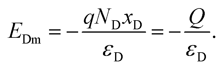
A triboelectric junction is a space charge region induced by the triboelectric effect, exhibiting characteristics similar to an abrupt heterojunction. In an abrupt heterojunction, the ion types in the space charge region change abruptly from positive ions to negative ions across the contact interface. Similarly, in a triboelectric junction, one material donates electrons while the other material accepts electrons, which also presents an abrupt change in ion type. Therefore, the analysis of a triboelectric junction can be analogous to the abrupt heterojunction.1,19,20 To simplify the analysis, we will discuss the triboelectric junction under a thermal equilibrium condition. Under this condition, the junction voltage represents the theoretical maximum junction voltage. In a triboelectric junction, the material that accepts (donates) electrons forms a negative (positive) ion zone with an ion concentration of NA (ND) (see Fig. 2a). The widths of the negative and positive ion zone are defined as xA and xD, respectively. The contact interface between the negative and positive ion zones is defined as x = 0. Thus, we obtain the charge density distribution, as shown in Fig. 2b: | (1) |
| qNAxA = qNDxD = Q, | (2) |
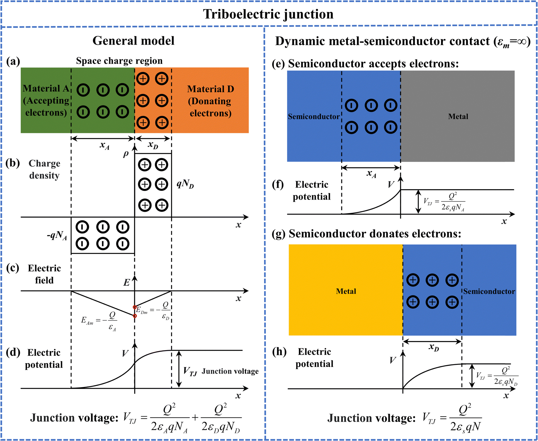 | ||
| Fig. 2 Formulaic analysis of the triboelectric junction. (a) The general model of the triboelectric junction; and the corresponding (b) charge density distribution; (c) electric field distribution (in a case that εA < εD); (d) electric potential distribution; (e) model and (f) electric potential distribution of dynamic metal–semiconductor contacts where the semiconductor accepts electrons; (g) model and (h) electric potential distribution of dynamic metal–semiconductor contacts where the semiconductor donates electrons. | ||
According to the Poisson equation,1,19,20 we obtain
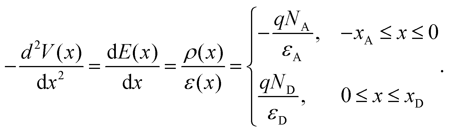 | (3) |
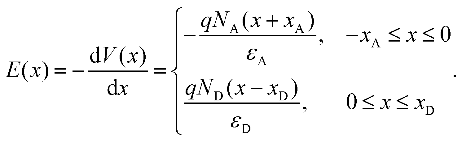 | (4) |
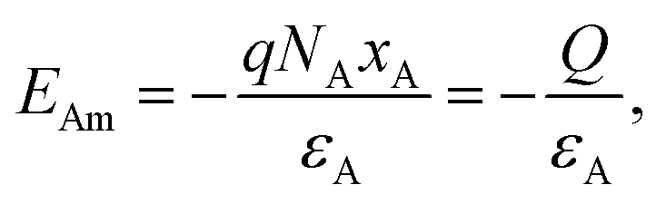 | (5) |
 | (6) |
Integrating eqn (4), we obtain the electric potential distribution, as shown in Fig. 2d:
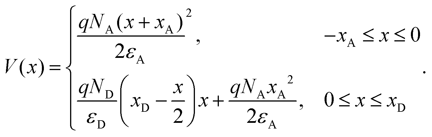 | (7) |
 | (8) |
The formulaic analysis provided above represents the general model of the triboelectric junction, including both dynamic semiconductor–semiconductor contacts and metal–semiconductor contacts. In dynamic semiconductor–semiconductor contacts with different contact materials, different dielectric-permittivity values are adopted, similar to abrupt heterojunctions. In dynamic semiconductor–semiconductor contacts using the same contact material but with different Fermi levels, the same dielectric-permittivity value is employed, similar to abrupt PN junctions. In dynamic metal–semiconductor contacts, the junction region is considered to exist solely within the semiconductor due to the infinite dielectric permittivity of metals (εm = ∞), similar to one-sided abrupt PN junctions (P+N junctions or PN+ junctions). In dynamic metal–metal contacts, the junction strength is considered negligible (εm = ∞). Dynamic contacts involving insulators are not discussed in the triboelectric junction model.
In dynamic metal–semiconductor contacts, the triboelectric junction can be divided into two categories and further simplified: (1) The semiconductor accepts electrons (see Fig. 2e, f, and Fig. S3, ESI†); and (2) The semiconductor donates electrons (see Fig. 2g, h and Fig. S3, ESI†). Eqn (8) can be reduced to
 | (9) |
Material's figure-of-merit of the triboelectric junction in metal–semiconductor contacts
The junction voltage is influenced by the parameters Q, εs, and N (see eqn (9)). To investigate the effect of a single parameter, the control variable method should be employed. In the case of studying the effect of Q, we can apply this method by using different metal materials to dynamically contact the same semiconductor material. This approach allows us to keep the values of εs and N constant, thereby isolating Q as the sole variable in the equation. If not specified, the subsequent discussion regarding the effect of Q is based on the aforementioned control variable method.Based on eqn (5), (6) and (9), we know that both the junction strength and junction voltage are positively correlated with Q (the triboelectric charge density). The triboelectric effect is a complex phenomenon21 that, so far, no equation can accurately express the generation of triboelectric charge. However, we can conclude that Q is related to the contact materials22,23 (kM), mechanical input14 (kI), and environmental factor24,25 (kE). Thus, we obtain
| Q = f(kM, kI, kE). | (10) |
Theoretically, the tendency of donating or accepting electrons in the triboelectric effect is determined by the electron affinity of the contact materials.26–29 The electron-affinity values of metals and semiconductors contribute to understanding the triboelectric junction. Electron affinity has also been studied in chemistry and semiconductor physics. However, the electron-affinity values in chemistry and semiconductor physics are characterized in a gaseous state and at a semiconductor–vacuum interface, respectively, and cannot be directly applied to the triboelectric effect in a solid–solid contact. The interatomic forces in a solid–solid contact are much stronger than those in a gaseous state or semiconductor–vacuum interface.
In electrochemistry, a metal reactivity series is established using the standard electrode potential30 to analyze the tendency of donating or accepting electrons between metals and other metal ions in solution (see Fig. S4 and Table S1, ESI†). In our experiments, we have found that the standard electrode potential can serve as a reference for electron affinity in analyzing the triboelectric junction. For example, in the semiconductor industry, the electrochemical displacement plating of metals like copper (Cu), silver (Ag), platinum (Pt), and gold (Au) on Si is commonly employed for junction depth examination, also known as junction delineation. In the junction delineation process, Si donates electrons, while metal ions in solution accept electrons,31,32 which is consistent with our experiment results that Si donates electrons and metals (Cu, Ag, Pt, and Au) accept electrons during dynamic contact. The possible reason is attributed to the chemical reactions that occur during tribology, known as mechanochemistry.33–37 The relative relationship of electron affinity between various metals and Si is also verified by experiments (see Fig. S5, ESI†). Therefore, we use the well-established standard electrode potential as a reference for the electron affinity when analyzing the dynamic metal–semiconductor contacts.
We introduce a material's figure-of-merit:38
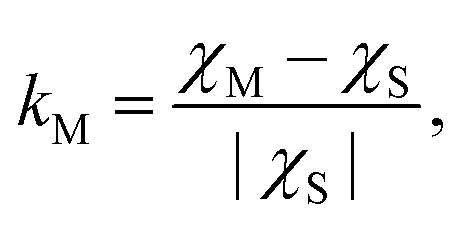 | (11) |
The junction direction determines the output polarity
The total junction at a dynamic interface has two components: one is the dominant triboelectric junction; the other is contributed by the intrinsic Fermi levels of the two contact materials. The triboelectric junction is a space charge region that dominates the electron–hole separation process. The junction direction determines the output polarity; the junction strength determines the output magnitude. Note that the term “output” in this work refers to the open-circuit voltage for convenience. Dynamic metal–Si contacts were utilized for verification, offering several advantages: (1) both metal and Si are single-element materials, whose electron-affinity values can refer to the standard electron potential; (2) the triboelectric junction is considered to exist solely within the Si region, as the dielectric permittivity of metal is infinite (εm = ∞); (3) non-equilibrium electron–hole generation only occurs in Si.The influence of junction direction on output polarity was investigated using various metal–Si contacts. When metals with electron-affinity values smaller than Si, such as magnesium (Mg), aluminum (Al), zinc (Zn), and tin (Sn), were used for dynamic metal–Si contact, the resulting outputs were negative. Conversely, when metals with electron-affinity values larger than Si, such as Cu, Ag, Pt, and Au, were involved in the dynamic metal–Si contact, positive outputs were observed (see Fig. 3a and Fig. S6, ESI†). From the perspective of kM, the output polarity is negative when χM− χS < 0, while it is positive when χM− χS > 0.
 | ||
| Fig. 3 The junction direction determines the output polarity. (a) The sign of χM− χS indicates both the junction direction and the resulting output polarity; (b) schematic diagram of the electron-cloud-potential-well model and (c) the triboelectric junction in a dynamic Al–Si contact; (d) dynamic Al–Si contacts generate negative outputs; (e) schematic diagram of the electron-cloud-potential-well model and (f) the triboelectric junction in a dynamic Cu–Si contact; (g) dynamic Cu–Si contacts generate positive outputs. | ||
We conducted further verification of the triboelectric junction using three representative materials (electron affinity: Al < Si < Cu, see Fig. 3b, c, e and f). Remarkably, we observed consistent output polarity when sliding the same metal material on Si wafers with different Fermi levels (see Fig. 3d and g). These Si wafers included heavily doped N-type Si wafer (N+ Si), N-type Si wafer (N Si), intrinsic Si wafer (I Si), P-type Si wafer (P Si) and heavily doped P-type Si wafer (P+ Si). This observation serves as strong evidence that the triboelectric junction dominates the electron–hole separation process. For Si wafers, the variation in Fermi levels was achieved through doping processes with different dopant types and concentrations.39–41 Note that the doping concentration in Si wafers is typically very low, even when they are heavily doped. In the context of Si wafers, a dopant concentration exceeding 0.1% is considered heavily doped. Therefore, the primary atoms that come into contact at the interface are still Si atoms and metal atoms. Hence, the triboelectric junction demonstrates its dominant role irrespective of the Fermi level of the Si wafers. Furthermore, we have confirmed the existence of the triboelectric junction not only in dynamic metal–semiconductor contacts but also in dynamic semiconductor–semiconductor contacts (see Fig. S7, ESI†). The working mechanism of three representative dynamic semiconductor-based contacts is shown in Fig. S8 (ESI†).
The junction strength determines the output magnitude
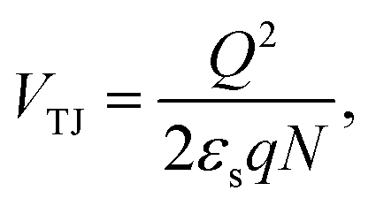
By referring to eqn (5) and (6), we can conclude the maximum junction strength as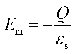 | (12) |
From eqn (12), we know that a larger Q results in a larger maximum junction strength. The junction voltage is the integral of the electric field across the junction region. Consequently, a larger Q will result in a larger junction voltage, as described in eqn (9). To directly investigate the effect of junction strength on the junction voltage, we can substitute eqn (12) into eqn (9), thereby establishing a relationship between the junction voltage and the maximum junction strength:
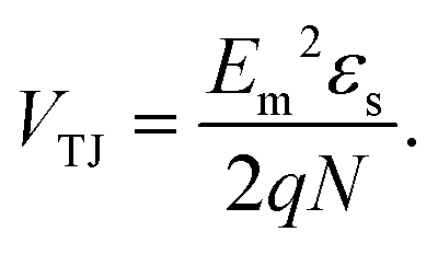 | (13) |
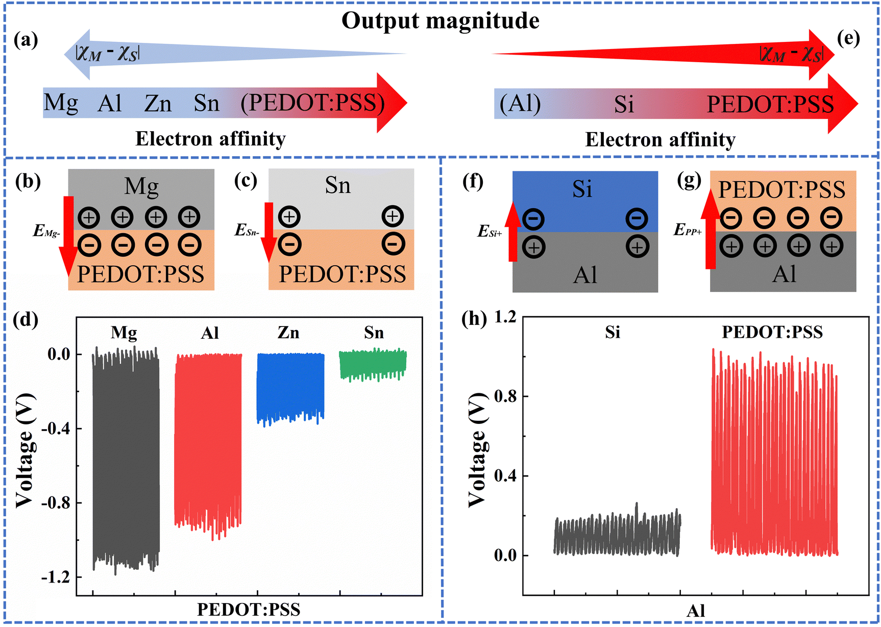 | ||
| Fig. 4 The junction strength determines the output magnitude. (a) For the negative output, a larger value of |χM− χS| contributes to a greater output magnitude; (b) the junction strength of the dynamic Mg-PEDOT:PSS contact is larger than that of (c) the dynamic Sn-PEDOT:PSS contact; (d) output magnitudes (negative) for dynamic metal-PEDOT:PSS contacts (|VMg−| > |VAl−| > |VZn−| > |VSn−|); (e) for the positive output, a larger value of |χM− χS| also contributes to a greater output magnitude; (f) the junction strength of the dynamic Si–Al contact is smaller than that of (d) the dynamic PEDOT:PSS-Al contact; (h) output magnitudes (positive) for dynamic semiconductor–Al contacts (VPP+ > VSi+). | ||
For negative output, when dynamically contacting with poly (3,4-ethylenedioxythiophene):poly (styrene sulfonate) (PEDOT:PSS), Mg exhibits a higher tendency to donate electrons compared to Sn. As a result, the dynamic Mg-PEDOT:PSS contact exhibits a higher junction strength than the dynamic Sn-PEDOT:PSS contact (junction strength: EMg− > ESn−, see Fig. 4b and c). Consequently, the output magnitude of the dynamic Mg-PEDOT:PSS contact exceeds that of the dynamic Sn-PEDOT:PSS contact. Further comparing different metals, we observe the following regularity of output magnitude: |VMg−| > |VAl−| > |VZn−| > |VSn−| (see Fig. 4d).
Similarly, for positive output, PEDOT:PSS demonstrates a greater propensity to accept electrons compared to Si when in dynamic contact with Al. This leads to a higher junction strength in the dynamic PEDOT:PSS-Al contact compared to the dynamic Si–Al contact (junction strength: EPP+ > ESi+, see Fig. 4f and g). Consequently, the output magnitude of the dynamic PEDOT:PSS-Al contact surpasses that of the dynamic Si–Al contact (see Fig. 4h). In the dynamic semiconductor–Al contacts (see Fig. 4h), the Al components are grounded. Note that the dynamic semiconductor–Al contacts shown in Fig. 4e–h deviate from strict adherence to the control variable method. The values of εs and N may vary when different semiconductor materials are used. However, it is worth mentioning that the output magnitude still exhibits a positive relationship with |χM− χS|. This implies that the electron affinity may have a more pronounced impact on determining the output magnitude compared to the influence of εs and N in this case. Theoretically, the effect of junction strength on the output magnitude is independent of polarity. In other words, irrespective of whether the polarity is negative or positive, a larger value of |χM− χS| contributes to a greater output magnitude.
Discussion
We successfully demonstrated that the triboelectric junction dominates the electron–hole separation process in dynamic metal–semiconductor contacts. Both the Schottky junction and the triboelectric junction involve a space charge region for electron–hole separation. However, they differ in their formation mechanisms. The Schottky junction is governed by the alignment of Fermi levels, while the triboelectric junction is induced by the much stronger triboelectric effect.14–16 Furthermore, the presence of a triboelectric junction also disrupts the dynamic equilibrium of charge movement necessary for maintaining an intrinsic Schottky junction or Ohmic contact, that is, the triboelectric charge induced by sliding affects the structure of the energy-band diagram.13 From the perspective of the “triboelectric junction” model, the complex coupling effect can be simplified as the influence of the Fermi level on the triboelectric junction. We have conducted a preliminary qualitative analysis of this coupling effect (see Fig. S9, ESI†). However, further investigation is necessary to develop a comprehensive theoretical model that fully considers this coupling effect. Additionally, the contribution of other effects, such as surface state,17,46 image force,47,48 tunneling,49 friction debris, and even mechanochemistry,33–37 can be further studied to optimize the model.The tribovoltaic effect has been extensively studied using various materials, including first-generation semiconductors (such as Si24), second-generation semiconductors (such as GaAs50), third-generation semiconductors (such as GaN14–16 and SiC51), organic polymers (such as PEDOT:PSS9,10 and polypyrrole11), and 2D materials (such as graphene,50 MoS2,8,52 Ta4C352 and Ti2C3Tx53), etc. Note that the derivation of the theoretical model is specially based on conventional inorganic semiconductor materials. However, we can infer that the concept of the triboelectric junction exists in most of the cases mentioned above. This inference is drawn from the definition that the triboelectric junction refers to the space charge region induced by the triboelectric effect, which is universal among almost all dynamic contacts. Nevertheless, whether the triboelectric junction plays a dominant role in the electron–hole separation process requires a detailed analysis of specific situations. For instance, in the case of 2D materials, further study is needed as some unique physical properties may exist at the atomically thin level.54,55
Materials and methods
Device fabrication and electrical characterization
All single-polished Si wafers (Zhejiang Lijing Silicon Material Co., Ltd, China) have the same crystal plane orientation [100] and thickness (500 μm). The resistivities of N+/P+ Si, N/P Si, and I Si are 0.001–0.005, 1–20, and >5000 Ω cm, respectively. A gold film is sputtered on the unpolished side of the Si wafer as a bottom electrode. The Si wafer was tailored into a rectangle (20 mm × 30 mm) for device fabrication. The rectangular Si, with an outgoing line on the bottom gold electrode, is attached to a PVC substrate. Different metal foils (Mg, Al, Zn, Sn, Cu, Ag, Pt, and Au) were tailored into a square (5 mm × 5 mm). Each metal foil is equipped with an outgoing line on the back side and then attached to PVC substrates. The PEDOT:PSS solution (Shanghai Ouyi Organic Photoelectric Material, OE-001) is drop-casted into a cleanroom wiper (20 mm ×![[thin space (1/6-em)]](https://www.rsc.org/images/entities/char_2009.gif) 30 mm) to form a PEDOT:PSS-textile composite. The composite is then dried in a 70 °C oven for 60 min. The PEDOT:PSS-textile composite was attached to a copper bottom electrode (Benyida Company, thickness 50 μm) on a PVC substrate. The open-circuit voltage was characterized by an oscilloscope (Rohde and Schwarzrte, RTE1024) under a normal force of 2 N. If not specified, the semiconductor component is grounded, except for the testing depicted in Fig. 4h. The output voltage of the intrinsic Si-based device was further processed to eliminate the baseline (usually tens of millivolts) induced by the photovoltaic effect (see Fig. S10, ESI†).
30 mm) to form a PEDOT:PSS-textile composite. The composite is then dried in a 70 °C oven for 60 min. The PEDOT:PSS-textile composite was attached to a copper bottom electrode (Benyida Company, thickness 50 μm) on a PVC substrate. The open-circuit voltage was characterized by an oscilloscope (Rohde and Schwarzrte, RTE1024) under a normal force of 2 N. If not specified, the semiconductor component is grounded, except for the testing depicted in Fig. 4h. The output voltage of the intrinsic Si-based device was further processed to eliminate the baseline (usually tens of millivolts) induced by the photovoltaic effect (see Fig. S10, ESI†).
Data availability
All data needed to evaluate the conclusions in this paper are present in the paper and/or the ESI.† Additional data and raw data are available upon request from the authors.Author contributions
ZY and XX conceived the project and designed the studies. XX performed experiments and analyzed the experimental data. ZY and XX wrote the manuscript. ZY and ZLW supervised the project.Conflicts of interest
The authors declare no competing interests.Acknowledgements
The work described in this paper was supported by General Research Grant (Project No. 11212021; 11210822) from the Research Grants Council of the Hong Kong Special Administrative Region.References
- S. M. Sze and K. K. Ng, Physics of Semiconductor Devices, Wiley, 2021 Search PubMed.
- Y. Wang, J. C. Kim, R. J. Wu, J. Martinez, X. Song, J. Yang, F. Zhao, A. Mkhoyan, H. Y. Jeong and M. Chhowalla, Nature, 2019, 568, 70–74 CrossRef CAS.
- P. C. Shen, C. Su, Y. Lin, A. S. Chou, C. C. Cheng, J. H. Park, M. H. Chiu, A. Y. Lu, H. L. Tang, M. M. Tavakoli, G. Pitner, X. Ji, Z. Cai, N. Mao, J. Wang, V. Tung, J. Li, J. Bokor, A. Zettl, C. I. Wu, T. Palacios, L. J. Li and J. Kong, Nature, 2021, 593, 211–217 CrossRef CAS.
- W. Schottky, Naturwissenschaften, 1938, 26, 843 CrossRef CAS.
- T. Harada, S. Ito and A. Tsukazaki, Sci. Adv., 2019, 5, eaax5733 CrossRef CAS PubMed.
- C. M. Went, J. Wong, P. R. Jahelka, M. Kelzenberg, S. Biswas, M. S. Hunt, A. Carbone and H. A. Atwater, Sci. Adv., 2019, 5, eaax6061 CrossRef CAS.
- Z. Zhang, D. Jiang, J. Zhao, G. Liu, T. Bu, C. Zhang and Z. L. Wang, Adv. Energy Mater., 2020, 10, 1903713 CrossRef CAS.
- J. Liu, A. Goswami, K. Jiang, F. Khan, S. Kim, R. McGee, Z. Li, Z. Hu, J. Lee and T. Thundat, Nat. Nanotechnol., 2018, 13, 112–116 CrossRef CAS.
- R. Yang, M. Benner, Z. Guo, C. Zhou and J. Liu, Adv. Funct. Mater., 2021, 31, 2103132 CrossRef CAS.
- J. Meng, Z. H. Guo, C. Pan, L. Wang, C. Chang, L. Li, X. Pu and Z. L. Wang, ACS Energy Lett., 2021, 6, 2442–2450 CrossRef CAS.
- J. Meng, C. Pan, L. Li, Z. H. Guo, F. Xu, L. Jia, Z. L. Wang and X. Pu, Energy Environ. Sci., 2022, 15, 5159–5167 RSC.
- R. Yang, R. Xu, W. Dou, M. Benner, Q. Zhang and J. Liu, Nano Energy, 2021, 83, 105849 CrossRef CAS.
- S. Lin and Z. L. Wang, Mater. Today, 2023, 62, 111–128 CrossRef CAS.
- Y. Chen, Z. Zhang, Z. Wang, T. Bu, S. Dong, W. Wei, Z. Chen, Y. Lin, Y. Lv, H. Zhou, W. Sun and C. Zhang, ACS Appl. Mater. Interfaces, 2022, 14, 24020–24027 CrossRef CAS PubMed.
- Z. Zhang, Z. Wang, Y. Chen, Y. Feng, S. Dong, H. Zhou, Z. L. Wang and C. Zhang, Adv. Mater., 2022, 34, 2200146 CrossRef CAS.
- Z. Wang, Z. Zhang, Y. Chen, L. Gong, S. Dong, H. Zhou, Y. Lin, Y. Lv, G. Liu and C. Zhang, Energy Environ. Sci., 2022, 15, 2366–2373 RSC.
- A. M. Cowley and S. M. Sze, J. Appl. Phys., 1965, 36, 3212–3220 CrossRef CAS.
- P. T. Landsberg, Solid-State Electron., 1975, 18, 1043–1052 CrossRef.
- W. Shockley, Bell Syst. Tech. J., 1949, 28, 435–489 CrossRef.
- E. Liu, B. Zhu and J. Luo, Semiconductor Physics, Publishing House of Electronics Industry, 2011 Search PubMed.
- Z. L. Wang and A. C. Wang, Mater. Today, 2019, 30, 34–51 CrossRef CAS.
- H. Zou, Y. Zhang, L. Guo, P. Wang, X. He, G. Dai, H. Zheng, C. Chen, A. C. Wang, C. Xu and Z. L. Wang, Nat. Commun., 2019, 10, 1427 CrossRef.
- H. Zou, L. Guo, H. Xue, Y. Zhang, X. Shen, X. Liu, P. Wang, X. He, G. Dai, P. Jiang, H. Zheng, B. Zhang, C. Xu and Z. L. Wang, Nat. Commun., 2020, 11, 2093 CrossRef CAS PubMed.
- Z. Wang, L. Gong, S. Dong, B. Fan, Y. Feng, Z. Zhang and C. Zhang, J. Mater. Chem. A, 2022, 10, 25230–25237 RSC.
- C. Xu, A. C. Wang, H. Zou, B. Zhang, C. Zhang, Y. Zi, L. Pan, P. Wang, P. Feng, Z. Lin and Z. L. Wang, Adv. Mater., 2018, 30, 1803968 CrossRef.
- G. Chen, C. Au and J. Chen, Trends Biotechnol., 2021, 39, 1078–1092 CrossRef CAS.
- X. Xiao, G. Chen, A. Libanori and J. Chen, Trends Chem., 2021, 3, 279–290 CrossRef CAS.
- A. Chen, C. Zhang, G. Zhu and Z. L. Wang, Adv. Sci., 2020, 7, 2000186 CrossRef CAS.
- R. Xu, Q. Zhang, J. Y. Wang, D. Liu, J. Wang and Z. L. Wang, Nano Energy, 2019, 66, 104185 CrossRef CAS.
- S. G. Bratsch, J. Phys. Chem. Ref. Data, 1989, 18, 1–21 CrossRef CAS.
- D. R. Turner, J. Electrochem. Soc., 1959, 106, 701 CrossRef CAS.
- N. Vivet, M. Diogo, A. Aubert, T. Moinet, F. Allanic, R. Perdreau and J.-P. Rebrassé, Mater. Sci. Appl., 2016, 07, 326–347 CAS.
- J. J. Gilman, Science, 1996, 274, 65 CrossRef CAS.
- Y. S. Zholdassov, L. Yuan, S. R. Garcia, R. W. Kwok, R. W. Carpick and A. B. Braunschweig, Science, 2023, 1058, 1053–1058 CrossRef PubMed.
- S. Wang, Y. Hu, T. B. Kouznetsova, L. Sapir, D. Chen, A. Herzog-arbeitman, J. A. Johnson, M. Rubinstein and S. L. Craig, Science, 2023, 1252, 1248–1252 CrossRef.
- T. Friščić, C. Mottillo and H. M. Titi, Angew. Chem., 2020, 132, 1030–1041 CrossRef.
- S. L. James and T. Frišcic, Chem. Soc. Rev., 2013, 42, 7494–7496 RSC.
- Y. Zi, S. Niu, J. Wang, Z. Wen, W. Tang and Z. L. Wang, Nat. Commun., 2015, 6, 8376 CrossRef CAS.
- T. I. Jeon and D. Grischkowsky, Phys. Rev. Lett., 1997, 78, 1106–1109 CrossRef CAS.
- E. Fourmond, M. Forster, R. Einhaus, H. Lauvray, J. Kraiem and M. Lemiti, Energy Procedia, 2011, 8, 349–354 CrossRef CAS.
- P. Kozodoy, H. Xing, S. P. DenBaars, U. K. Mishra, A. Saxler, R. Perrin, S. Elhamri and W. C. Mitchel, J. Appl. Phys., 2000, 87, 1832–1835 CrossRef CAS.
- Z. He, C. Zhong, X. Huang, W. Y. Wong, H. Wu, L. Chen, S. Su and Y. Cao, Adv. Mater., 2011, 23, 4636–4643 CrossRef CAS PubMed.
- J. Luo, H. Wu, C. He, A. Li, W. Yang and Y. Cao, Appl. Phys. Lett., 2009, 95, 043301 CrossRef.
- B. Qi and J. Wang, J. Mater. Chem., 2012, 22, 24315–24325 RSC.
- N. K. Elumalai and A. Uddin, Energy Environ. Sci., 2016, 9, 391–410 RSC.
- S. Lin, R. Shen, T. Yao, Y. Lu, S. Feng, Z. Hao, H. Zheng, Y. Yan and E. Li, Adv. Sci., 2019, 6, 1901925 CrossRef CAS.
- C. R. Crowell and S. M. Sze, Solid-State Electron., 1966, 9, 1035–1048 CrossRef CAS.
- C. Y. Chang and S. M. Sze, Solid-State Electron., 1970, 13, 727–740 CrossRef.
- V. L. Rideoutt, Solid-State Electron., 1970, 13, 993–1009 CrossRef.
- S. Lin, Y. Lu, S. Feng, Z. Hao and Y. Yan, Adv. Mater., 2019, 31, 1804398 CrossRef PubMed.
- J. Xia, X. Luo, J. Li, L. Zhu and Z. L. Wang, ACS Appl. Mater. Interfaces, 2022, 14, 55192–55200 CrossRef CAS.
- B. Fan, Z. Wang, G. Liu, Z. Wang, X. Fu, L. Gong and C. Zhang, Adv. Funct. Mater., 2023, 33, 2301821 CrossRef CAS.
- X. Luo, L. Liu, Y. C. Wang, J. Li, A. Berbille, L. Zhu and Z. L. Wang, Adv. Funct. Mater., 2022, 32, 2113149 CrossRef CAS.
- K. F. Mak, C. Lee, J. Hone, J. Shan and T. F. Heinz, Phys. Rev. Lett., 2010, 105, 136805 CrossRef PubMed.
- Y. Xuan, H. Chen, Y. Chen, H. Zheng, Y. Lu and S. Lin, Research, 2020, 2020, 3850389 CrossRef CAS PubMed.
Footnote |
| † Electronic supplementary information (ESI) available. See DOI: https://doi.org/10.1039/d3ee02870d |
| This journal is © The Royal Society of Chemistry 2024 |