Rare three-valence-band convergence leading to ultrahigh thermoelectric performance in all-scale hierarchical cubic SnTe†
Received
30th July 2023
, Accepted 7th November 2023
First published on 9th November 2023
Abstract
Band convergence is an important approach for improving the thermoelectric performance, as it can significantly increase the Seebeck coefficient without obviously sacrificing the electrical conductivity. Herein, we report a rare three-valence-band convergence achieved in doped p-type cubic SnTe to enhance the power factor and obtain a record-high ZT. Ternary MnCdTe2 alloying activates the lower-energy-lying Λ valence band (with a large degeneracy of Nv = 8), and additional Ge doping promotes energy alignment between the Λ and L bands, leading to a rare three-valence-band (i.e., L, Σ and Λ) convergence that pronouncedly enhances the power factor (PF = 29.3 μW cm−1 K−2 at 900 K). Ge doping also greatly enhances the solid solubility of MnCdTe2 in the SnTe matrix and effectively tunes the precipitate size, producing all-scale hierarchical structures, which generate a full spectrum of phonon scattering, especially low-frequency acoustic–optical scattering, leading to an ultralow lattice thermal conductivity (κL = 0.26 W m−1 K−1 at 670 K). Collectively, this gives a record-high ZT of 1.97 at 900 K and an average ZTave of 0.8 in the temperature range of 300 to 900 K for 8% MnCdTe2-doped SnTe with 3.2% Ge. Furthermore, a single-leg TE module based on (SnTe)0.92(MnCd0.6Ge0.4Te2)0.08 outputs a power density of 800 mW cm−2 for a ΔT of 446 K, which is competitive with those of devices based on state-of-the-art mid-temperature materials (600–900 K) within the same ΔT, demonstrating great potential for future applications.
Broader context
Thermoelectric (TE) devices, which can directly convert exhaust heat into useful electrical energy, have been considered an alternative renewable energy resource to relieve the deterioration of the environment. Historically, tin telluride (SnTe) has underperformed its chalcogenide analogues GeTe/PbTe in TE performance due to its less favourable band structure and relatively high lattice thermal conductivity. However, SnTe is a promising alternative to both GeTe and PbTe due to its earth-abundant and environmentally friendly characteristics. Herein, we demonstrate a synergistic strategy that can simultaneously decouple the transport of carriers and phonons through dual incorporation of MnCdTe2 and Ge, eventually yielding a record-high peak ZT of 1.97 with a high average ZTave of 0.8 in the temperature range from 300 to 900 K. This significant advance is realized by three-valence-band charge transport enabled by MnCdTe2 alloying and all-scale phonon scattering centre construction via further Ge incorporation. Beyond the two-band convergence paradigm, we demonstrate that a third Λ valence band with a degeneracy Nv of ∼8 could be activated through the addition of MnCdTe2 into the SnTe matrix, contributing to a three-band (L, Σ and Λ valence band) transport behaviour. Moreover, the incorporation of Ge improves the solid solubility of Mn and Cd simultaneously, which can effectively refine the MnCdTe2 precipitate size, induce significant strain and then provide additional κlat attenuation. Both theoretical and experimental results reveal that the produced artificially hierarchical structures and intensified acoustic–optical phonon scattering provide full-spectrum phonon scattering, leading to an ultralow lattice thermal conductivity of 0.26 W m−1 K−1 at 676 K. The fabricated single-leg TE device based on (SnTe)0.92(MnCd0.6Ge0.4Te2)0.08 shows a promising output power density of 800 mW cm−2 for a temperature difference of 446 K, showing promising potential for mid-high-temperature heat harvesting.
|
1. Introduction
Thermoelectric (TE) materials, which can enable direct conversion between heat and electricity, have drawn wide scientific attention.1 Generally, the TE performance is determined by the dimensionless figure of merit ZT = S2σT/(κe + κL), where S, σ, T, κe, and κL denote the Seebeck coefficient, electrical conductivity, absolute temperature, electronic thermal conductivity and lattice thermal conductivity, respectively.2 In practice, a superior ZT is demanded to simultaneously achieve a high power factor (PF) and low thermal conductivity κT,3 which are strongly interrelated by the carrier concentration (nH) and electronic structure. Any optimization regarding a single parameter is always accompanied by a suppression effect on the other two parameters.4 Benefiting from the relatively independent correlations of the valley degeneracy (Nv) and carrier mobility (μ), convergence of separate valleys can increase S without substantially degrading σ (limited intervalley scattering).5 As each pocket contributes to the PF in roughly an additive manner, inducing an energy approach of isolated band extrema at different symmetry points in the Brillouin zone can contribute to a very high PF. To improve the material TE performance, effective strategies are typified by the enlargement of PF through band structure manipulation5 and nH dynamic optimization6 as well as by the suppression of κL through the introduction of defects.7 These strategies have been successfully implemented in Bi2Te3,8 IV–VI compounds,9 filled skutterudites,10 Zintl phases,11etc. Moreover, remarkable success was also achieved in exploring and synthesizing novel high-performance TE compounds, such as CsAg5Te3,12 CsCu5Se313 and KCu5Se3.14
Tin telluride, SnTe, with a rock-salt crystal structure has been regarded as a potential mid-temperature alternative to the state-of-the-art compounds PbTe and GeTe due to its nontoxic and earth-abundant characteristics.15 However, the abundant vacancies in pristine SnTe induce an extremely high hole density on the order of 1020–1021 cm−3, resulting in high κE, low S and consequently inferior ZT.16 In addition, the large energy offset (ΔEV ≈ 0.3 eV) between the light L and heavy Σ valence bands limits the full contribution of the heavy Σ valence band, which further inhibits the achievement of high S.17–19 Thermally, SnTe possesses a small bandgap (0.18 eV), which induces severe bipolar conduction at the temperatures of interest (700–900 K). The key approaches for further enhancing the electrical transport performance of SnTe-based materials mainly rely on valence band convergence,20 which can be achieved by reducing the energy offset between light and heavy valence bands through alloying with various substitutions.21–25 For instance, alloying selenide with SnTe can increase the energy of the Σ valence band relative to the primary L valence band.21 In contrast, cation-site alloying with monotellurides, such as MnTe,22 MgTe,23 SrTe,24 HgTe16 and PbTe,25 can effectively decrease the energy of the L valence band relative to the secondary Σ valence band. In fact, engineering orbital interactions to obtain high Nv has been a critical strategy for seeking promising ZT not only in tin and lead chalcogenides, but also in skutterudites, Zintl phases, GeTe, etc. Thus, converging additional valence bands with the L and Σ bands is rationally expected to achieve further ZT improvement in SnTe. However, constricted by the excessive band energy offset and limited dopant solubility, extra transport band activation is extremely challenging. Furthermore, because the room-temperature κL (3 W m−1 K−1) of SnTe is well above its amorphous limit (0.4 W m−1 K−1),26 strenuous efforts have been made to enhance ZT by minimizing κL. Construction of different scale defects, such as second-phase nanoprecipitates,20 interstitial atoms,27 entropy engineering,28 cation vacancies29 and nanoscale planar gaps,30 has been proven to be effective strategies for suppressing the κL in SnTe. Generally, due to the negative correlation between the precipitate size and surface-to-volume ratio in multicomponent systems, small precipitates have a higher phonon scattering efficiency for reducing κL than large precipitates. However, few studies have achieved κL engineering through precipitate size manipulation, although it is an effective scheme to regulate lattice thermal transport. Therefore, elaborately designing the microstructure is critical for synergistic enhancement of the TE properties by integrating the abovementioned electrical transport optimization strategy.
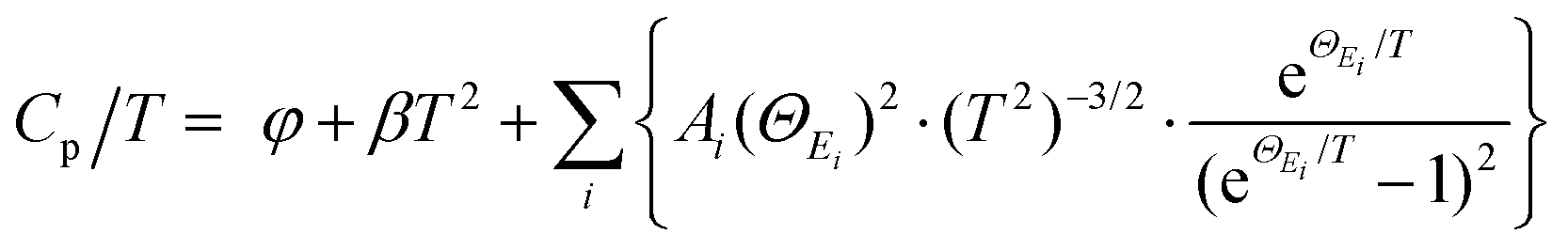
Applying Mn or Cd substitution at Sn sites has been demonstrated to be the most effective approach for minimizing the valence band offset in SnTe-based materials. In particular, Cd can significantly reduce the energy separation to 0.12 eV at only a 3% doping concentration.20 Additionally, both Mn and Cd possess an eminent ability to nanostructure the SnTe matrix, contributing to optimized κL.20,21 However, due to their limited solubility (∼9% for Mn and ∼3% for Cd), a single agent is insufficient for completely converging the valence bands. This motivates the current study to explore synergistic alloying strategies to fully optimize the charge transport properties. In this work, an effective strategy was shown to activate a more degenerate Λ valence band (Nv = 8) by alloying MnCdTe2 in a SnTe matrix, leading to rare three-band (L, Σ and Λ valence band) transport behaviour for the first time in the SnTe-based materials. The ternary MnCdTe2 activates the Λ valence band, as shown in Fig. 1a. The additional Ge doping at the Cd site promotes energy alignment between the Λ and L bands, contributing to an enhanced S ∼ 62 μV K−1 at room temperature. Consequently, complete three-band convergence is realized in (SnTe)0.92(MnCd0.6Ge0.4Te2)0.08. Furthermore, Ge doping moderately enhances the solubility of ternary MnCdTe2 in the SnTe matrix; as a result, the size of the precipitates is effectively tuned, producing an all-scale artificially hierarchical structure, which enables full-spectrum phonon scattering (Fig. 1b). Moreover, the calculated phonon dispersions demonstrate that MnCdTe2 alloying induces intensified acoustic–optical phonon scattering, which intrinsically decreases the phonon relaxation time. All these factors contribute to an ultralow κL of 0.26 W m−1 K−1 at 676 K. This simultaneous optimization of μW and κL significantly increases μW/κL (Fig. 1c) and then the material quality factor B (Fig. 1d). Consequently, a record-high ZT of ∼1.97 is realized at 900 K. Furthermore, a single-leg TE device based on (SnTe)0.92(MnCd0.6Ge0.4Te2)0.08 outputs a promising output power density of 800 mW cm−2 for a temperature difference (ΔT) of 446 K, which is superior to that of similar modules based on state-of-the-art mid-temperature materials with the same ΔT, demonstrating promising potential for applications.
 |
| | Fig. 1 (a) Schematic diagram of the multivalence band evolution in SnTe as the dopant concentration varies. The Nv values of the L band, Λ band and Σ band are 4, 8 and 12, respectively. (b) Schematic hierarchical structures in (SnTe)0.92(MnCd0.6Ge0.4Te2)0.08. (c) Composition dependence of μW/κL at 300 K and 900 K, and obtained minimum κL. (d) Maximum ZT and optimal η versus material quality factor B, revealing the optimal doping level. | |
2. Results and discussion
2.1 Design and synthesis of the (SnTe)0.92(MnCd0.6Ge0.4Te2)0.08 material
Based on the Hume–Rothery rule, the impurity solubility is dominated by the atomic radius difference and electronegativity difference of the solute and solvent.31 Compared to CdTe or MnTe, the cationic size and electronegativity of MnCdTe2 are closer to those of SnTe, which is beneficial for forming a continuous solid solution. Hence, we adopted the ternary compound MnCdTe2 as an alloying candidate. Specifically, a series of (SnTe)1−x(MnCdTe2)x samples were synthesized to engineer the TE performance. A nominal concentration range of MnCdTe2 (0–10%) was introduced into the SnTe matrix (Fig. S1, ESI†) until the optimal fraction (8%) was confirmed (Fig. S2, ESI†). When Cd exceeds its solubility limit (3%), coarse Cd-containing precipitates tend to form in spinodal decomposition processes, which may lead to disturbance of carrier transport and thermal shorting, ultimately destroying the composite performance.16,21 Hence, to realize effective κL reduction, the size distribution and growth process of precipitates must be refined and regulated. According to previous literature,32,33 the solubilities of Mn and Cd in the SnTe matrix can both be improved by the introduction of Ge. Therefore, the synergistic codoping element Ge was rationally incorporated at the Cd site, which was expected to further refine the MnCdTe2 precipitate size and provide additional κL attenuation (Fig. S3 and S4, ESI†).
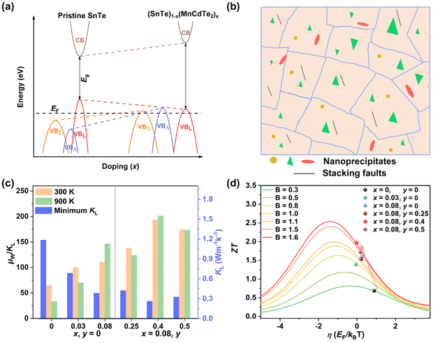
Details of the synthesis, characterization, TE property measurements, and density functional theory (DFT) calculations are given in the ESI.†Fig. 2a shows the room-temperature powder X-ray diffraction (PXRD) patterns taken for the (SnTe)1−x(MnCd1−yGeyTe2)x samples, where the major reflection peaks can be well indexed to the single rock-salt SnTe phase with a space group of Fm![[3 with combining macron]](https://www.rsc.org/images/entities/char_0033_0304.gif) m. Several impurity diffraction peaks corresponding to the secondary MnCdTe2 phase appear at 23 and 39 degrees. The lattice parameter linearly decreases with increasing x for x ≤ 0.08, suggesting successful incorporation of MnCdTe2 into the SnTe matrix (Fig. 2b).33,34 The reduction in the lattice parameter originates from the smaller ionic size of Mn2+ (∼0.66 Å) compared with those of Cd2+ (∼0.97 Å) and Sn2+ (∼0.93 Å). The precipitation process of the secondary phase could be accelerated by increasing x, as shown in Fig. S1 (ESI†). With an increase in y, the compositional dependence of the lattice parameter deviates upwards from the linear relationship. This deviation suggests that the decreasing rate of the lattice parameter slows with the introduction of Ge, indicating an increase in Cd dissolution. As Fig. S3 (ESI†) shows, the intensity of the impurity reflection peak at 23 degrees decreases with increasing y, suggesting the dissolution of MnCdTe2 upon Ge doping. The stability of the (SnTe)0.92(MnCd0.6Ge0.4Te2)0.08 sample was confirmed by temperature-dependent XRD measurements over the temperature range of 300 to 933 K (Fig. S5, ESI†). The precipitation phase composition and morphology were studied by scanning electron microscopy (SEM). Taking (SnTe)0.92(MnCd0.6Ge0.4Te2)0.08 as an example, the backscattered electron (BSE) image of a polished surface shown in Fig. 2c reveals a high density of unique triangle-shaped nanoscale precipitates embedded in mesoscale grains, and stripe precipitates are segregated at the grain boundaries. The energy-dispersive spectroscopy (EDS) maps depicting the elemental distribution in Fig. S6 (ESI†) clearly show the segregation behaviour of Mn and Cd, with the EDS compositions of the matrix and precipitates given in Fig. S7 (ESI†). In contrast, the Ge-free sample (x = 0.08, y = 0) exhibits much larger MnCdTe2 precipitates (Fig. S8, ESI†). A specific comparative analysis of the microstructures of the Ge-free and Ge-included samples is shown in Fig. S9 (ESI†), which indicates significant precipitate refinement induced by Ge incorporation. Specifically, the statistical average size of the precipitates dramatically decreases from 2.82 μm for the Ge-free sample to 0.22 μm for the Ge-included sample (Fig. S10, ESI†). Moreover, BSE imaging was conducted on several different regions of the (SnTe)0.92(MnCd0.6Ge0.4Te2)0.08 sample (Fig. S11, ESI†), revealing widely distributed nanoprecipitates. All these results indicate that the solubility limit of Cd in the SnTe matrix was promoted by Ge doping, in agreement with a previous report.33 To further investigate the microstructure, electron backscatter diffraction (EBSD) was applied to determine the grain size and grain boundary distribution. The EBSD crystal-orientation map (Fig. 2d) and grain boundary map (Fig. S12a, ESI†) reveal a mixed microstructure and a multiple-scale grain size distribution. As displayed in Fig. S12b and d (ESI†), the statistical average grain sizes of (SnTe)0.92(MnCd0.6Ge0.4Te2)0.08 and (SnTe)0.92(MnCdTe2)0.08 estimated by the circular approximation are 5.8 μm and 7.0 μm, respectively. Moreover, the crystal-orientation map (Fig. 2d) enables direct observation of the precipitated MnCdTe2 phase distribution at the boundary region.
m. Several impurity diffraction peaks corresponding to the secondary MnCdTe2 phase appear at 23 and 39 degrees. The lattice parameter linearly decreases with increasing x for x ≤ 0.08, suggesting successful incorporation of MnCdTe2 into the SnTe matrix (Fig. 2b).33,34 The reduction in the lattice parameter originates from the smaller ionic size of Mn2+ (∼0.66 Å) compared with those of Cd2+ (∼0.97 Å) and Sn2+ (∼0.93 Å). The precipitation process of the secondary phase could be accelerated by increasing x, as shown in Fig. S1 (ESI†). With an increase in y, the compositional dependence of the lattice parameter deviates upwards from the linear relationship. This deviation suggests that the decreasing rate of the lattice parameter slows with the introduction of Ge, indicating an increase in Cd dissolution. As Fig. S3 (ESI†) shows, the intensity of the impurity reflection peak at 23 degrees decreases with increasing y, suggesting the dissolution of MnCdTe2 upon Ge doping. The stability of the (SnTe)0.92(MnCd0.6Ge0.4Te2)0.08 sample was confirmed by temperature-dependent XRD measurements over the temperature range of 300 to 933 K (Fig. S5, ESI†). The precipitation phase composition and morphology were studied by scanning electron microscopy (SEM). Taking (SnTe)0.92(MnCd0.6Ge0.4Te2)0.08 as an example, the backscattered electron (BSE) image of a polished surface shown in Fig. 2c reveals a high density of unique triangle-shaped nanoscale precipitates embedded in mesoscale grains, and stripe precipitates are segregated at the grain boundaries. The energy-dispersive spectroscopy (EDS) maps depicting the elemental distribution in Fig. S6 (ESI†) clearly show the segregation behaviour of Mn and Cd, with the EDS compositions of the matrix and precipitates given in Fig. S7 (ESI†). In contrast, the Ge-free sample (x = 0.08, y = 0) exhibits much larger MnCdTe2 precipitates (Fig. S8, ESI†). A specific comparative analysis of the microstructures of the Ge-free and Ge-included samples is shown in Fig. S9 (ESI†), which indicates significant precipitate refinement induced by Ge incorporation. Specifically, the statistical average size of the precipitates dramatically decreases from 2.82 μm for the Ge-free sample to 0.22 μm for the Ge-included sample (Fig. S10, ESI†). Moreover, BSE imaging was conducted on several different regions of the (SnTe)0.92(MnCd0.6Ge0.4Te2)0.08 sample (Fig. S11, ESI†), revealing widely distributed nanoprecipitates. All these results indicate that the solubility limit of Cd in the SnTe matrix was promoted by Ge doping, in agreement with a previous report.33 To further investigate the microstructure, electron backscatter diffraction (EBSD) was applied to determine the grain size and grain boundary distribution. The EBSD crystal-orientation map (Fig. 2d) and grain boundary map (Fig. S12a, ESI†) reveal a mixed microstructure and a multiple-scale grain size distribution. As displayed in Fig. S12b and d (ESI†), the statistical average grain sizes of (SnTe)0.92(MnCd0.6Ge0.4Te2)0.08 and (SnTe)0.92(MnCdTe2)0.08 estimated by the circular approximation are 5.8 μm and 7.0 μm, respectively. Moreover, the crystal-orientation map (Fig. 2d) enables direct observation of the precipitated MnCdTe2 phase distribution at the boundary region.
 |
| | Fig. 2 (a) XRD patterns and (b) lattice parameter for (SnTe)1−x(Mn1−yCdyTe2)x samples, with a comparison to those of Sn1−xCdxTe33 and Sn1−xMnxTe.34 (c) BSE image and (d) EBSD crystal-orientation map for the high-performance (SnTe)0.92(MnCd0.6Ge0.4Te2)0.08 sample. | |
2.2. TE performance
To uncover the effects of MnCdTe2 alloying and Ge doping on the TE properties, the TE performance of the (SnTe)1−x(MnCd1−yGeyTe2)x samples was measured (Fig. 3 and Fig. S4, ESI†). σ exhibits a decreasing tendency with increasing T, indicating degenerate semiconducting behaviour (Fig. 3a). With the incorporation of MnCdTe2 and Ge, σ is significantly suppressed. For instance, the room-temperature σ of pristine SnTe is 8037 S cm−1, which significantly decreases to 2635 S cm−1 in the (SnTe)0.92(MnCd0.6Ge0.4Te2)0.08 sample. Considering the enhanced nH, this σ decrease is reasonably attributed to the large μH reduction, as shown in Fig. S14a (ESI†). Meanwhile, the DFT calculations reveal that the Sn vacancy formation energy presents a decreasing tendency with increasing concentrations of MnCdTe2 and Ge, which accounts for the nH increment (Fig. S14b, ESI†). As displayed in Fig. 3b, S is significantly improved over the entire temperature range with the incorporation of MnCdTe2 and Ge. Typically, the room-temperature S is dramatically increased from 19 μV K−1 in pristine SnTe to 62 μV K−1 in (SnTe)0.92(MnCd0.6Ge0.4Te2)0.08 despite the simultaneous nH increment. S increases up to 206 μV K−1 at 900 K in the (SnTe)0.92(MnCd0.6Ge0.4Te2)0.08 sample, with no obvious intrinsic excitation occurring. Both MnCdTe2 alloying and Ge doping provide benefits for enhancing S, with essentially different mechanisms; MnCdTe2 alloying particularly activates the low-lying Λ band, leading to an increase in Nv and eventually  , whereas Ge doping contributes to further alignment of the L, Λ and Σ valence bands. Detailed discussions will be given below. Benefiting from the S enhancement and the retainment of a moderate σ, the PF values of (SnTe)1−x(MnCd1−yGeyTe2)x are obviously improved over the whole temperature range, with a maximum of 29.3 μW cm−1 K−2 at 900 K realized by the (SnTe)0.92(MnCd0.6Ge0.4Te2)0.08 sample, which is enhanced by approximately 45% compared with that of pristine SnTe (Fig. 3c). This PF value is strongly competitive with that of all the reported Mn/Cd-containing SnTe-based materials (Fig. S15, ESI†). Furthermore, anomalies in transport properties are observed in samples containing Ge around 600–700 K. These anomalies can be reasonably attributed to decreased contributions from the heavy valence bands, which occur as a result of carrier redistribution at elevated temperatures.32 The temperature-dependent total thermal conductivity (κT) of the (SnTe)1−x(MnCd1−yGeyTe2)x samples is shown in Fig. 3d. κL is calculated by subtracting the electronic component κe from κT, where κe is estimated by the Wiedemann–Franz equation, κe = LσT, with the Lorenz number (L) determined by the single parabolic band (SPB) model with acoustic phonon scattering, and κe remarkably decreases upon doping due to the significant σ reduction (Fig. S16a, ESI†). Similarly, MnCdTe2 alloying and Ge doping also substantially suppress κT and κL. For instance, the room-temperature κT decreases from 6.5 W m−1 K−1 in SnTe to 2.65 W m−1 K−1 in (SnTe)0.92(MnCd0.6Ge0.4Te2)0.08, and the room-temperature κL declines from 2.87 to 0.99 W m−1 K−1. On the other hand, κL initially decreases and then gradually increases with increasing Ge content, reaching its minimum values at y = 0.4. This indicates that there is an optimal volume fraction of precipitates for the most effective phonon scattering.7 Details are provided in Fig. S16b (ESI†). Owing to the PF enhancement and the significant κT suppression, ZT obviously improves over the whole temperature range and peaks at 900 K for (SnTe)0.92(MnCd0.6Ge0.4Te2)0.08 with a value of 1.97 (Fig. 3f). This impressive TE performance is highly reproducible (Fig. S17, ESI†), with outstanding cycling stability (Fig. S18, ESI†) that is comparable to that of the state-of-the-art PbTe-based materials.5
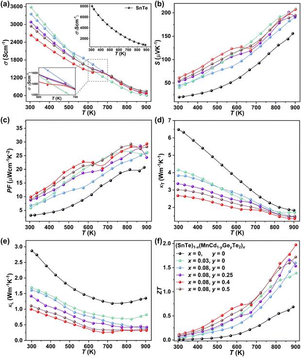 |
| | Fig. 3 Temperature dependence of (a) σ, (b) S, (c) PF, (d) κT, (e) κL and (f) ZT for the (SnTe)1−x(MnCd1−yGeyTe2)x samples. | |
2.3. Electronic structures of (SnTe)1−x(MnCd1−yGeyTe2)x
To further reveal the underlying reasons for the S enhancement and maintenance of a decent σ, the electronic band structures and density of states (DOS) of (SnTe)1−x(MnCd1−yGeyTe2)x were investigated by DFT calculations. (More details are provided in the ESI.†) As Fig. 4a illustrates, pristine SnTe presents an energy offset of 0.29 eV between the L and Σ points and a direct bandgap of 0.1 eV at the L point, in accordance with previous reports.35 In sharp contrast, Sn23Mn2CdGeTe27 exhibits an energy reduction of the L band but an elevation of the Σ band that leads to a nearly vanishing energy offset (ΔE1–2), giving rise to a strong band convergence between the L and Σ bands. Beyond the conventional two-band convergence between the L and Σ bands22 or the Λ and Σ bands,28 the lower-lying Λ valence band (labelled as 3 in Fig. 4a) is also activated and aligns well with both the L and Σ bands, indicating a highly desired yet rare three-band convergence. This additional involvement of the highly degenerate Λ band for charge carrier transport enables a large DOS effective mass  without obviously damaging the carrier mobility, which explains the S and PF enhancement observed in Fig. 3. The generation of an extra valence band leads to obvious DOS enlargement near the valence band edge, which is an indicator of
  increment (Fig. S19, ESI†). This enlargement is very different from the DOS modifications previously observed in PbTe and GeTe, which derived largely from DOS distortion.36,37 Furthermore, band structure studies also show bandgap enlargement and valence band flattening (Fig. 4a and b) since the incorporation of Mn2+, Cd2+ and Ge2+ cations at the Sn2+ site is expected to increase the ionicity of the material, which in turn enlarges the bandgap and flattens the band dispersion. Typically, with the incorporation of MnCdTe2 and Ge, the bandgap widens from 0.1 eV in SnTe to 0.2 eV in Sn23Mn2CdGeTe27 (Fig. 4b), which is consistent with the experimental trend (Fig. S20, ESI†). Generally, bandgap widening can effectively suppress the bipolar effect in charge transport and improve S. In addition, the L valence band flattening (Fig. 4a) can be well understood when the relationship between Eg and the effective mass near the band edge
  is considered.
  is associated with the Eg variation under the plane-wave approximation, expressed by eqn (1):
| | 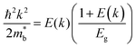 | (1) |
where k is the wave vector and E(k) represents the electron dispersion. Thus, the widening Eg implies an increase in  .
.  can also be defined by eqn (2):
| | 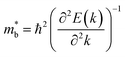 | (2) |
 |
| | Fig. 4 (a) Band structures of Sn27Te27 and Sn23Mn2CdGeTe27 with inclusion of spin–orbit coupling (SOC). The three-valence band-convergence related bands at L, Σ and Λ are labelled as 1, 2 and 3, respectively. And the degeneracy of some black bands are Nv(Σ) = 12, Nv(Λ) = 8, and Nv(L) = 4. (b) Calculated energies of VBL, VBΣ, VBΛ, CBL and Eg as a function of the alloying content. Temperature-dependent RH (c) and Pisarenko relationship of S (d), Pisarenko relationship of μH (e) and component-dependent md* (f) at 302 and 772 K for the (SnTe)1−x(MnCd1−yGeyTe2)x samples. | |
Eqn (2) shows that an increased  portends band edge flattening. Thus, Eg widening eventually flattens the valence band. As illustrated in Fig. 4b and Fig. S21 (ESI†), 3.85% MnCdTe2 alloying in SnTe (i.e., Sn25MnCdTe27) has a prominent effect of raising the Λ band in comparison with MnTe alloying with a higher concentration (Sn25Mn2Te27). To get close to experimental practice, Sn24Mn2CdTe27 and Sn23Mn2CdGeTe27 were also calculated for contrast. Fig. 4b presents the dynamic evolution of the multivalence bands, revealing complete three-band convergence induced by the dual alloying of MnCdTe2 and Ge. In particular, Ge doping slightly reduces the band offset (ΔE3–1) between the L and Λ bands (Fig. 4a) and improves the room-temperature S (Fig. 3b).
Qualitative insights into the atomic-level contributions were revealed by the orbital-projected band structures of Sn23Mn2CdGeTe27 (Fig. S22, ESI†). In agreement with the previous statements based on tight binding (TB) calculations,38–41 Sn23Mn2CdGeTe27 exhibits an atypical metavalent bonding (MVB) feature, the valence band maximum (VBM) of which is mainly dominated by the bonding interactions of Sn-p and Te-p along with the antibonding interaction between Sn-s and Te-p (Fig. S22a, ESI†). As seen, Mn-d is responsible for the modulation of the Λ valence band (Fig. S22b, ESI†), which was also observed in Sn0.75Ge0.05Mn0.2Te(Cu2Te)0.05.28 Specifically, Pei et al. demonstrated that with the assistance of 5% GeTe, a two-band convergence between the Λ and Σ bands can be realized in SnTe by high concentration (20%) MnTe alloying; unfortunately, the energy of the L band was decreased too much to provide transport anymore.28 The composition-dependent valence band edge positions were measured by ultraviolet photoelectron spectroscopy (UPS). As shown in Fig. S23 (ESI†), the valence band edge moves deeper from 4.02 eV in SnTe to 4.27 eV in (SnTe)0.92(MnCd0.6Ge0.4Te2)0.08, which agrees well with the DFT calculation results shown in Fig. 4b.
To experimentally confirm this valence band evolution, the temperature-dependent Hall coefficients (RH) were measured (Fig. 4c). Pristine SnTe presents an obvious RH peak at 770 K, which is a typical sign of the multiband character in rock-salt chalcogenides,34 indicating carrier redistribution between the light and heavy valence bands. With the introduction of MnCdTe2 (x = 0.03, 0.08), the RH temperature dependences are significantly weakened. Together with Ge doping (x = 0.08, y = 0.4, 0.5), RH is nearly constant until 600 K, indicating single-band transport behaviour. This is in accordance with the DFT band structure featuring a rare three-valence-band convergence, which exhibits transport behaviour similar to that for an effective single band. The obvious RH peak reduction is rationally attributed to the decrease in the mobility ratio between the light and heavy valence bands associated with L band flattening (Fig. 4a) as well as to the  increase. Furthermore, the dominant scattering mechanism in all the (SnTe)1−x(MnCd1−yGeyTe2)x samples still obeys acoustic phonon scattering, as the temperature-dependent μH curves reveal (Fig. S24 and S25, ESI†).
The Pisarenko curves based on the SPB model are shown in Fig. 4d and e to present the electronic transport properties of the (SnTe)1−x(MnCd1−yGeyTe2)x samples. Note that the validity of the SPB approximation is guaranteed by the highly converged three valence bands and the dominant acoustic phonon scattering. A similar SPB approximation was also adopted for some other multiple-band chalcogenides, such as GeTe,37 AgSbTe242 and SnSe.43Fig. 4d presents the S–nH curves, on which the experimental data at 302 K and 772 K are marked. From (x = 0, y = 0) to (x = 0.08, y = 0.4), the upward tendency of the S–nH curves strongly indicates md* enhancement upon dual x, y doping since the S–nH curve is mainly influenced by md* within the SPB model.44 Correspondingly, the md* variations are given in Fig. 4f and present a dramatic md* enhancement at 302 K from 0.2 me with (x = 0, y = 0) to 1.9 me with (x = 0.08, y = 0.4). These md* values are much higher than those of SnTe materials with a single dopant, such as Cd,33 Mn,32 Mg,23 and Ca.45 Due to the md* and nH enhancement, the μH–nH curves present a downward trend (Fig. 4e). In addition, introducing MnCdTe2 (x) has a significant influence on nH at lower temperatures (Fig. S14, ESI†) in this work, suggesting the multiple band activation character. In contrast, further Ge doping only slightly regulates the energy of the L band, which shows a relatively weak influence on nH. The weighted mobility (μW) can well evaluate the electronic quality in terms of the band structure that is closely related to  and
and  . As shown in Fig. S26 (ESI†), the μW values of the (SnTe)1−x(MnCd1−yGeyTe2)x samples are superior to that of the pristine SnTe sample in the whole temperature range, which could help explain the overall PF enhancement. The obviously improved μW is an indicator of electronic structure evolution in this work. To explicitly proclaim such an evolution, the nH-dependent S and μH are plotted in Fig. S27 (ESI†), in which the theoretically calculated two-band model results as well as the available data reported for the related SnTe-based materials are also presented for comparison. The S values of our (SnTe)1−x(MnCd1−yGeyTe2)x samples are obviously higher than the two-band model values, suggesting a modified valence band structure and an increased
  . Further inspection reveals that our samples also present larger S values than those of the SnTe samples doped by a single element (i.e., Ge, Cd, Mn22,31,33), a dual element (i.e., Ge/Cd33), or a simple alloy (GeMnTe2,46 CdSe47) at a specific nH value. Moreover, our (SnTe)1−x(MnCd1−yGeyTe2)x samples have μH values higher than those under the two-band transport conditions at a given nH, indicating increased electronic conduction channels, further supporting the multiple-valence-band convergence character (Fig. S27b, ESI†).
2.4. DFT phonon calculations
To investigate the fundamentals related to lattice dynamics, DFT phonon dispersion calculations were conducted. The phonon dispersions of pristine SnTe and MnCdTe2-alloyed SnTe were calculated based on the supercell models of Sn8Te8 and Sn6MnCdTe8, respectively. As shown in Fig. 5a, the resonant bonding characteristic derived from the long-range interaction associated with the intrinsic polarization in the octahedrally coordinated rock-salt-type structure makes the low-frequency transverse optical (TO) phonons soften at the Γ point and then leads to acoustic phonon scattering by the TO mode, which mainly moderates κL.48 The corresponding projected phonon density of states (PDOS) in Fig. 5d illustrates that in pristine SnTe, Sn or Te dominates the low-frequency or high-frequency phonons, respectively, with the lowest-frequency peak located at 1.51 THz. In contrast, in the ternary MnCdTe2-alloyed SnTe, extra low-lying optical phonons overlap with the acoustic phonon branches, enhancing the optical–acoustic phonon scattering and leading to a stronger lattice anharmonicity. Clearly, this kind of low-frequency region shift of the optical modes suggests strong optical–acoustic coupling; for instance, the lowest-frequency TO branch is significantly reduced from 1.1 to 0.75 THz (Fig. 5a vs. b), with a shift of the lowest-frequency peak from 1.51 to 1.26 THz (Fig. 5d vs. e) from Sn8Te8 to Sn6MnCdTe8, respectively. To reveal the origin of additional optical modes in Sn6MnCdTe8, the atomic vibrations around the Γ point of the lowest-frequency optical mode (optical #1, marked in Fig. 5b) are visualized in Fig. 5c, which clearly demonstrates that Cd with a remarkably large displacement from its equilibrium position gives rise to a strong Cd vibration that perturbs the Te atoms, leading to a Te-octahedron distortion, which in turn produces the additional low-frequency optical modes. These analyses are in good agreement with the PDOS results (Fig. 5e), indicating that Cd contributes to the low-frequency region, whereas Mn contributes mainly to the high-frequency region.
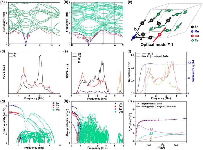 |
| | Fig. 5 DFT phonon dispersions for (a) Sn8Te8 and (b) Sn6MnCdTe8. (c) Atomic vibrations in the primitive cell for low-frequency optical mode #1 of Sn6MnCdTe8. PDOS of Sn8Te8 (d) and Sn6MnCdTe8 (e). (f) Normalized total DOS and frequency dependence of the cumulative lattice thermal conductivity. Calculated phonon group velocity (ν) for (g) Sn8Te8 and (h) Sn6MnCdTe8. (i) Measured CP/T as a function of T2 for (SnTe)0.92(MnCd0.6Ge0.4Te2)0.08. | |
In addition to the phonon anharmonicity enhancement induced by optical–acoustic scattering, the available three-phonon scattering phase space is another decisive factor for the phonon lifetimes. Generally, three-phonon scattering dominates the thermal resistance for acoustic (a) and optical (o) phonons in bulk materials, with the most important scattering channels involving three acoustic phonons (aaa), one acoustic phonon combined with two optical phonons (aoo) and two acoustic phonons combined with one optical phonon (aao). The phase-space volume in IV–VI compounds has been well demonstrated to be dominated by (aoo) and (aao) processes.48 Considering the momentum and energy conservation requirements in the scattering process, the optical mode downshift widens the (aoo) scattering channel and provides more chances for scattering of the low-frequency acoustic modes. Note that the downshift of optical modes decreases the Debye frequency (the maximum frequency of the acoustic modes) from 1.45 to 1.35 THz (Fig. 5a vs. b) and then flattens the acoustic branches, giving a phonon group velocity (ν) reduction. As shown in Fig. 5g and h, MnCdTe2 alloying reduces ν, which is in accordance with the experimental observation of the sound velocity (Fig. S30, ESI†). Moreover, compared with Sn8Te8, Sn6MnCdTe8 presents a remarkable redshift in the phonon DOS (Fig. 5f), manifesting a significant phonon softening effect. The representative frequency of 1.0 THz in SnTe is responsible for 90% of the cumulative κL, indicating that the low-frequency phonon in SnTe dominates the thermal transport. This scenario further demonstrates that the Cd-induced low-frequency optical phonons and phonon softening significantly contribute to κL reduction, and a similar phenomenon has also been observed in other TE compounds, such as InTe,49 CsCu4Se3,50 and YbFe4Sb12,51 exhibiting ultralow lattice thermal conductivity.
Generally, the extra optical modes give rise to specific heat in excess of the Debye contribution at low temperatures, which can be experimentally probed through the low-temperature heat capacity and analysed by the Debye–Einstein model (eqn (3)):52
| |  | (3) |
where
φ and
β represent the electronic term and Debye term, respectively, and the last summation term signifies the contribution of the localized Einstein oscillator modes that represent the low-frequency phonon modes. Taking the high-performance sample (SnTe)
0.92(MnCd
0.6Ge
0.4Te
2)
0.08 as a typical example, the measured
Cp data can be sufficiently described by neither the single Debye mode nor the Debye + 1 Einstein mode (Fig. S30, ESI
†) but by one Debye mode and two Einstein oscillators (
Fig. 5i) in the full temperature range from 2 to 19 K (fitting parameters are given in Table S2, ESI
†). Further observations reveal that the Einstein modes contribute more than half of the total
Cp, whereas the Debye mode starts to dominate in the relatively high-temperature region, which strongly corroborates the existence of extra low-frequency phonons that play a key role in the heat transport of (SnTe)
0.92(MnCd
0.6Ge
0.4Te
2)
0.08.
2.5. Novel microstructures in (SnTe)0.92(MnCd0.6Ge0.4Te2)0.08
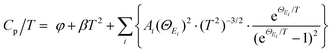
To further reveal the structural origin of the suppressed κL obtained in the optimized (SnTe)0.92(MnCd0.6Ge0.4Te2)0.08 sample, transmission electron microscopy (TEM) studies were performed to investigate the microstructures. As expected from the existing phase diagram and our design principle, low-magnification dark-field TEM images reveal numerous multiscale nanoprecipitates (indicated by red arrows) within each grain of the SnTe matrix (Fig. 6a). The precipitates appear as triangles (Fig. 6a) and circles (Fig. S31 and S32, ESI†) with a size distribution range of 50 to 300 nm. EDS indicates that the precipitates are enriched in Mn and Cd and severely deficient in Sn, suggestive of a MnCdTe2 phase (Fig. 6d1–d5). Meanwhile, slight deficiency of Te and enrichment of Mn and Ge in the core region of the precipitates can be observed, indicating inhomogeneous heterostructures of the precipitates. The medium-magnification TEM images in Fig. 6e present one typical nanoprecipitate with bright contrast embedded in the SnTe matrix. According to the electron diffraction contrast, several different regions can be discovered in the sample, that is, the SnTe matrix, the principal part of the precipitate, the transition interface (∼30 nm) between the matrix and precipitate and the core region phase. The indexing of the fast Fourier transform (FFT) pattern from the precipitate further confirms its cubic MnCdTe2 structure, as shown in the bottom left of Fig. 6e. As shown in Fig. 6g, the selected area electron diffraction (SAED) pattern along [001] obtained from the matrix verifies its rock-salt structure. The SAED patterns taken along [001] from the SnTe matrix and the areas with precipitates are given in Fig. 6h. Clearly, slight diffraction spot splitting can be observed far from the central transmission beam, which can be attributed to the similar crystal structures and lattice parameters of SnTe (Fmm, a = 6.32 Å) and MnCdTe2 (Fm![[4 with combining macron]](https://www.rsc.org/images/entities/char_0034_0304.gif) m, a = 6.41 Å). Furthermore, the lattice mismatch between the SnTe matrix and MnCdTe2 precipitate can be identified as 3% by analysing the SAED patterns. Therefore, corresponding interfacial complexation between the matrix and precipitates is expected to form to compensate for the lattice distortion.53 To gain further insights, we conducted atomic-resolution aberration-corrected STEM to visualize the atomic arrangement and additional details in the interface region. As shown in Fig. 6b, a clean coherent interface without any complexation along the [1
m, a = 6.41 Å). Furthermore, the lattice mismatch between the SnTe matrix and MnCdTe2 precipitate can be identified as 3% by analysing the SAED patterns. Therefore, corresponding interfacial complexation between the matrix and precipitates is expected to form to compensate for the lattice distortion.53 To gain further insights, we conducted atomic-resolution aberration-corrected STEM to visualize the atomic arrangement and additional details in the interface region. As shown in Fig. 6b, a clean coherent interface without any complexation along the [1![[1 with combining macron]](https://www.rsc.org/images/entities/char_0031_0304.gif) 2] direction between SnTe(110) and MnCdTe2(110) is formed because of the similar lattice parameters and compatible atom arrangement. However, high εxy strain centred around the corresponding interface can still be spatially captured by geometric phase analysis (GPA), as shown in Fig. 6c. This can be understood by the heterogeneous chemical bonds between the SnTe matrix and MnCdTe2 precipitate. Specifically, SnTe adopts MVB; however, MnCdTe2 presents covalent bonding, resulting in diverse physical properties, such as the Born effective charge, effective coordination number and force constant.39,54–56 These discrepancies will lead to high local strain around the heterointerfaces.9 In addition to the local interfacial strain, dispersed lattice strains can also be observed within the whole MnCdTe2 precipitate (Fig. 6c and Fig. S33, ESI†), and a possible mechanism can be attributed to the generation of nanoscale twins and stacking faults (discussed later). This is very different from conventional nanocomposites, in which strain centres usually gather around phase boundaries rather than distributing throughout the whole grain.21,57–59 These widely distributed lattice strains can effectively suppress phonon propagation, leading to a significant κL reduction. Moreover, semicoherent interfaces along the [12] direction between SnTe(110) and MnCdTe2(110) are formed due to enlarged atomic mismatch (Fig. 6j). Correspondingly, nanoscale twins and twin boundaries are formed in the MnCdTe2 boundary region due to the need to reduce the interfacial energy. Compared to the significant discontinuity that could arise, nanoscale twins only result in a very small variation in the structure, and the extra energy on the junction plane is not significantly different from that on any other plane within the crystal.60 Therefore, these twins can be easily formed and remain stable in the sample. The twin boundaries are distributed at the atomic scale (<1 nm) and could thus provide effective scattering for high-frequency phonons. According to previous reports, Cd tended to precipitate out from the matrix and form coarse precipitates when exceeding its solid solubility limit, which was widely observed in the PbTe/SnTe–CdTe system.16,21,47,61 Usually, such large precipitates are inefficient at scattering heat-carrying phonons due to the low surface-to-volume ratio.16,57 As discussed above, Ge incorporation obviously refines the precipitate size due to the improved solid solubility degree, contributing to more effective phonon scattering. Moreover, obvious stacking faults (indicated by yellow arrows) can be found in the MnCdTe2 precipitate region (Fig. 6(f)) and the transition interface region (inset in Fig. 6(e)). Enlarged views of the stacking faults in regions k and l are presented in Fig. 6k and l, respectively. The stretched linear stripes existing in the FFT patterns precisely reflect the structural features of the disarranged regions of the stacking sequence. In fact, these stacking faults are several nanometres in width and tens of nanometres in length and could thus significantly scatter phonons from medium to short wavelengths while having a relatively weak influence on charge transport. Notably, such stacking faults are widely present in the triangular precipitates in different bulk regions of the (SnTe)0.92(MnCd0.6Ge0.4Te2)0.08 sample (Fig. S34, ESI†). Apart from these nanoscale features, the abovementioned SEM-BSE and EBSD images exhibit the presence of uniformly distributed micron-sized precipitates and mesoscale grain boundaries throughout the bulk matrix. Therefore, all-scale artificially hierarchical architectures are formed in the (SnTe)0.92(MnCd0.6Ge0.4Te2)0.08 sample, which can effectively scatter phonons at all length scales in SnTe-based materials.
2] direction between SnTe(110) and MnCdTe2(110) is formed because of the similar lattice parameters and compatible atom arrangement. However, high εxy strain centred around the corresponding interface can still be spatially captured by geometric phase analysis (GPA), as shown in Fig. 6c. This can be understood by the heterogeneous chemical bonds between the SnTe matrix and MnCdTe2 precipitate. Specifically, SnTe adopts MVB; however, MnCdTe2 presents covalent bonding, resulting in diverse physical properties, such as the Born effective charge, effective coordination number and force constant.39,54–56 These discrepancies will lead to high local strain around the heterointerfaces.9 In addition to the local interfacial strain, dispersed lattice strains can also be observed within the whole MnCdTe2 precipitate (Fig. 6c and Fig. S33, ESI†), and a possible mechanism can be attributed to the generation of nanoscale twins and stacking faults (discussed later). This is very different from conventional nanocomposites, in which strain centres usually gather around phase boundaries rather than distributing throughout the whole grain.21,57–59 These widely distributed lattice strains can effectively suppress phonon propagation, leading to a significant κL reduction. Moreover, semicoherent interfaces along the [12] direction between SnTe(110) and MnCdTe2(110) are formed due to enlarged atomic mismatch (Fig. 6j). Correspondingly, nanoscale twins and twin boundaries are formed in the MnCdTe2 boundary region due to the need to reduce the interfacial energy. Compared to the significant discontinuity that could arise, nanoscale twins only result in a very small variation in the structure, and the extra energy on the junction plane is not significantly different from that on any other plane within the crystal.60 Therefore, these twins can be easily formed and remain stable in the sample. The twin boundaries are distributed at the atomic scale (<1 nm) and could thus provide effective scattering for high-frequency phonons. According to previous reports, Cd tended to precipitate out from the matrix and form coarse precipitates when exceeding its solid solubility limit, which was widely observed in the PbTe/SnTe–CdTe system.16,21,47,61 Usually, such large precipitates are inefficient at scattering heat-carrying phonons due to the low surface-to-volume ratio.16,57 As discussed above, Ge incorporation obviously refines the precipitate size due to the improved solid solubility degree, contributing to more effective phonon scattering. Moreover, obvious stacking faults (indicated by yellow arrows) can be found in the MnCdTe2 precipitate region (Fig. 6(f)) and the transition interface region (inset in Fig. 6(e)). Enlarged views of the stacking faults in regions k and l are presented in Fig. 6k and l, respectively. The stretched linear stripes existing in the FFT patterns precisely reflect the structural features of the disarranged regions of the stacking sequence. In fact, these stacking faults are several nanometres in width and tens of nanometres in length and could thus significantly scatter phonons from medium to short wavelengths while having a relatively weak influence on charge transport. Notably, such stacking faults are widely present in the triangular precipitates in different bulk regions of the (SnTe)0.92(MnCd0.6Ge0.4Te2)0.08 sample (Fig. S34, ESI†). Apart from these nanoscale features, the abovementioned SEM-BSE and EBSD images exhibit the presence of uniformly distributed micron-sized precipitates and mesoscale grain boundaries throughout the bulk matrix. Therefore, all-scale artificially hierarchical architectures are formed in the (SnTe)0.92(MnCd0.6Ge0.4Te2)0.08 sample, which can effectively scatter phonons at all length scales in SnTe-based materials.
 |
| | Fig. 6 Precipitates and planar defects in the (SnTe)0.92(MnCd0.6Ge0.4Te2)0.08 sample. (a) Low-magnification dark-field TEM image with red arrows marking the triangular precipitates. (b) Atomic-scale structure of the interface between SnTe(100) and MnCdTe2(100). (c) GPA of the region in (b). (d1)–(d5) Corresponding EDS mappings of region d. (e) Medium-magnification TEM images of a typical triangular precipitate. The insets present enlarged views of region i. (f) HRTEM image of region (e) with yellow arrows marking the stacking faults. SAED patterns along [001] taken from the local matrix region without precipitates (g) and a relatively larger region that includes precipitates (h). (j) Atomic-scale structure of region j in (e); the inset shows the inverse fast Fourier transform (IFFT) of the box region. (k) Enlarged view of region k in (f), and (l) enlarged view of region l in (f); the insets present the corresponding FFT images that confirm the presence of stacking faults. | |
2.6. Thermal transport properties and TE device
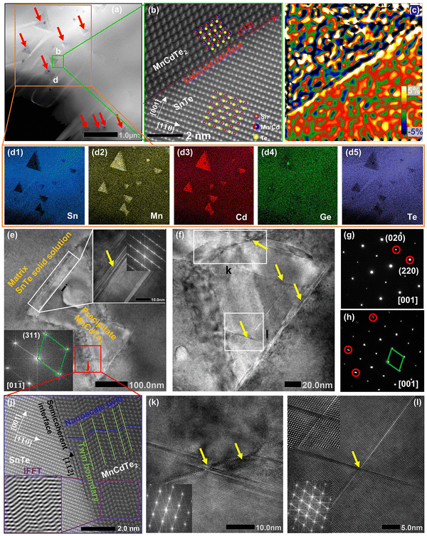
To further clarify the mechanism underlying the largely suppressed κL, quantitative analyses were conducted to reveal the phonon scattering sources. Generally, the sound velocity (ν) in a solid material, which is directly determined by the chemical bond strength, can well reflect the propagation speed of the lattice vibrations.29 The composition dependences of the average sound velocity (νa) and the Grüneisen parameter (γ) are given in Fig. 7a, all of which were estimated from the experimental longitudinal and transverse sound velocities measured at room temperature (Fig. S30 and Table S2, ESI†). As the MnCdTe2 alloying concentration increases, νa presents an obvious downwards trend, and γ rapidly increases, showing good agreement with the DFT phonon calculations. This trend indicates apparent lattice softening, which enhances the Umklapp process and lattice anharmonicity. Meanwhile, for both the Umklapp and normal processes, the phonon scattering rates are proportional to γ2, and the γ increase indicates enhancement of the anharmonic phonon–phonon interactions. νa and γ slightly change with Ge codoping, suggesting that the Ge dopant introduces another mechanism that also contributes to the κL reduction. According to kinetic theory, κL in a solid is closely related to the heat capacity (CV), sound velocity (ν) and phonon lifetime (τ) via κL = 1/3CVνa2τ; thus, the κL reduction should originate from the decrease in the phonon lifetime, which in turn confirms the efficacy of abundant hierarchical structures in suppressing κL.
 |
| | Fig. 7 (a) Composition-dependent average sound velocity (νa) and Grüneisen parameter (γ). (b) Spectral lattice thermal conductivity κS of the (SnTe)0.92(MnCd0.6Ge0.4Te2)0.08 sample at 302 K. (c) Calculated κL as a function of temperature involving various phonon scattering mechanisms. The symbols represent the experimental κL, and the solid line represents the Callaway model results. (d) Comparison between the minimum κL obtained in this work and the literature results.15,16,20–23,30,32,67 The dashed line represents the theoretical minimum κL of SnTe predicted by the Born–von Karman periodic boundary condition.68 (e) Temperature-dependent ZT values for (SnTe)0.92(MnCd0.6Ge0.4Te2)0.08 in comparison with those of some high-performance SnTe alloys in previous reports.15,20–22,25,26,29,32,69–71 (f) Output power density (Pout, solid symbols) and output voltage (Vout, hollow symbols) as a function of the current under different temperature differences (ΔT) for a single-leg (SnTe)0.92(MnCd0.6Ge0.4Te2)0.08 device. | |
To qualitatively evaluate how the optical–acoustic phonon scattering and micro/nanohierarchical structures influence the heat transport in the high-performance (SnTe)0.92(MnCd0.6Ge0.4Te2)0.08 sample, a phenomenological Debye–Callaway model was employed, according to which κL in a crystalline solid can be expressed by eqn (4):62,63
| | 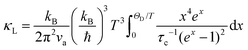 | (4) |
where
ħ is the reduced Planck constant,
kB is the Boltzmann constant,
ΘD is the Debye temperature,
νa is the average sound velocity,
x is the reduced phonon energy and can be expressed as
ħω/
kBT, and
τc is a frequency-dependent phonon scattering relaxation time determined by the addition of the participating phonon scattering processes. Accordingly, we consider the phonon–phonon Umklapp scattering (U),
τU, grain boundary scattering (B),
τB, normal process (N),
τN, point defect scattering (PD),
τPD, nanoprecipitate phonon scattering (NP),
τNP, stacking fault scattering (SF),
τSF, and acoustic–optical phonon scattering (AO),
τAO, as the main scattering sources. According to Matthiessen's rule, the total relaxation time can be expressed as
eqn (5):
64,65| | | τc−1 = τU−1 + τN−1 + τB−1 + τPD−1 + τNP−1 + τSF−1 + τAO−1 | (5) |
The detailed calculations and associated parameters are given in Table S3 (ESI†). Applying the specified τc (eqn (6)) and taking the obtained optimal fitting parameters, κL was calculated based on the seven different scattering mechanisms, among which the U + N-estimated κL for SnTe and the U + N + B + PD + NP + SF + AO-estimated κL for (SnTe)0.92(MnCd0.6Ge0.4Te2)0.08 illustrate good agreement with the corresponding experimentally observed values (Fig. 7c). Correspondingly, the domain between two adjacent lines symbolizes the κL reduction magnitude caused by introducing an additional scattering process. As seen, a sharp κL reduction is induced by the incorporation of NP and SF and should be a major cause for the obviously suppressed κL. Moreover, AO also makes a considerable contribution to the κL reduction and significantly pushes the κL of (SnTe)0.92(MnCd0.6Ge0.4Te2)0.08 to ultralow values. The integrand spectral lattice thermal conductivity (κS) can be expressed as eqn (6),65
| | 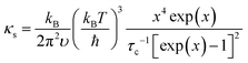 | (6) |
which reveals the contribution of various scattering sources to
κL at various phonon frequencies (
Fig. 7b). As shown, NP and SF strongly scatter the high-frequency phonons, while AO is effective for phonons at middle frequencies, and grain boundaries are the main scattering source for low-frequency phonons. Additionally, point defects are responsible for high-frequency phonon scattering. As a result of phonon scattering at all length scales, an ultralow
κL of 0.26 W m
−1 K
−1 is achieved at 670 K.
As illustrated in Fig. 7d, the minimum κL achieved here is one of the lowest values compared to the related literature results of SnTe-based compounds involving Ge/Mn/Cd components,15,16,23,30,66,67 for instance, 0.56 W m−1 K−1 at 823 K in SnCd0.03Te(CdS)0.02,20 0.43 W m−1 K−1 at 572 K in Sn0.83Mn0.17Te,22 0.36 W m−1 K−1 at 900 K in Sn0.83Ge0.05Mn0.2Te(Cu2Te)0.0532 and 0.36 W m−1 K−1 at 873 K in SnAg0.05Te(CdSe)0.1.21 These results strongly manifest that sufficient κL reduction can be realized in the solid solution of (SnTe)1−x(MnCd1−yGeyTe2)x by introducing abundant hierarchical nano/mesostructures and low-frequency optical modes to scatter phonons at all scales. ZT is proportional to the quality factor (B), which can be calculated with eqn (7):49
| | 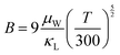 | (7) |
where
μW is an
nH-independent quantity, which can essentially quantify the number and mobility parameter (
μ0) of conduction channels for charge carrier transport.
68 Consequently, the decoupling effect (
i.e., net increment) of the dual incorporation of MnCdTe
2 and Ge in SnTe can be rationally evaluated by the ratio
μW/
κL. As shown in
Fig. 1c, the
μW/
κL value significantly increases from 33.5 for SnTe to 201.3 for (SnTe)
0.92(MnCd
0.6Ge
0.4Te
2)
0.08, which indicates that the band evolution and artificially hierarchical structures in this work can effectively impede thermal conduction and concurrently optimize charge transport. Benefiting from the alignment of activated multiple valence bands and significantly suppressed thermal conductivity, the achieved peak
ZT of 1.97 (
Fig. 7e) is a record for all the reported SnTe-based TEs and highly competitive with that of lead chalcogenides.
15,20–22,25,26,29,32,69–71 Moreover, to evaluate the expected TE device efficiency of (SnTe)
0.92(MnCd
0.6Ge
0.4Te
2)
0.08, the average
ZT (
ZTavg) was estimated by
eqn (8):
| | 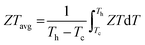 | (8) |
As shown in Fig. S35 (ESI
†), a largely improved
ZTavg of 0.8 is obtained between 300 and 900 K. To further explore the power generation ability, we prepared a single-leg TE device with Ni as the metal electrode (
Fig. 8). The device power generation properties were tested and are given in
Fig. 7f. As shown, the good linearity of the current (
I)
versus output voltage (
V) indicates good ohmic contact. A promising output power density (
Pout) of 800 mW cm
−2 is obtained at a
Th of 570 K and a Δ
T of 446 K for a single-leg device made of (SnTe)
0.92(MnCd
0.6Ge
0.4Te
2)
0.08. Additionally, compared with the literature data of other typical mid-temperature TE modules (SnTe,
28 GeTe,
72 and PbTe
73), the obtained
Pmax of 800 mW cm
−2 is competitive, showing promising potential for mid-high-temperature heat harvesting (Fig. S36, ESI
†).
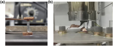 |
| | Fig. 8 (a) Photograph of the single leg device. (b) Experimental setup for the device performance measurement. | |
3. Conclusion
In summary, we reveal a rare three-valence-band convergence in the dual-doped p-type cubic SnTe material (with MnCdTe2 ternary and Ge elements) that synergistically decouples the carrier and phonon transport. The DFT electronic band structure analyses reveal that the MnCdTe2 alloying effectively activates the Λ valence band with a large degeneracy Nv = 8 and that the Ge doping promotes energy alignment between the Λ and L bands, which together lead to the three-band convergence associated with a pronounced valence band flattening and bandgap enlargement. This optimized band structure enhances the weighted mobility, significantly enlarges S, and eventually results in a superior PF = 29.3 μW cm−1 K−2. In addition, the phonon dispersion curves reveal strong coupling between the low-frequency optical modes and the heat-carrying acoustic modes, which effectively enhances the phonon scattering phase space volume and reduces the phonon lifetime. Additionally, such unique dual incorporation of MnCdTe2 ternary and Ge elements produces novel all-scale hierarchical structures leading to an ultralow κL = 0.26 W m−1 K−1 at 670 K. Consequently, (SnTe)0.92(MnCd0.6Ge0.4Te2)0.08 realizes a record high ZT = 1.97 at 900 K and a ZTave = 0.8 in the temperature range of 300 to 900 K. Moreover, a single-leg TE module based on this material outputs a power density of 800 mW cm−2 for a ΔT of 446 K, which is strongly competitive with those of devices based on typical mid-temperature (600–900 K) TE materials within the same ΔT, demonstrating great potential for future applications.
Conflicts of interest
The authors declare no competing financial interest.
Acknowledgements
This research was supported by the National Key R&D Program of China (2022YFB3803902) and the National Natural Science Foundation of China under projects 21975032 and 52172128. The authors would like to thank Mrs. Yang Zhang for her support in transmission electron microscopy from the Instrumental Analysis Center of Xi’an Jiaotong University.
References
- G. J. Snyder and E. S. Toberer, Nat. Mater., 2008, 7, 105–114 CrossRef CAS PubMed.
- J. He and T. M. Tritt, Science, 2017, 357, 1360–1369 CrossRef.
- L.-D. Zhao, V. P. Dravid and M. G. Kanatzidis, Energy Environ. Sci., 2014, 7, 251–268 RSC.
- R. Moshwan, L. Yang, J. Zou and Z.-G. Chen, Adv. Funct. Mater., 2017, 27, 1703278 CrossRef.
- Y. Z. Pei, X. Y. Shi, A. LaLonde, H. Wang, L. D. Chen and G. J. Snyder, Nature, 2011, 473, 66–69 CrossRef CAS PubMed.
- Y. Xiao, Y. Wu, P. Nan, H. Dong, Z. Chen, Z. Chen, H. Gu, B. Ge, W. Li and Y. Pei, Chem, 2020, 6, 523–537 CAS.
- J. R. Sootsman, R. J. Pcionek, H. J. Kong, C. Uher and M. G. Kanatzidis, Chem. Mater., 2006, 18, 4993–4995 CrossRef CAS.
- Y. Pan, Y. Qiu, I. Witting, L. G. Zhang, C. G. Fu, J. W. Li, Y. Huang, F. H. Sun, J. Q. He, G. J. Snyder, C. Felser and J. F. Li, Energy Environ. Sci., 2019, 12, 624–630 RSC.
- K. Biswas, J. He, I. D. Blum, C.-I. Wu, T. P. Hogan, D. N. Seidman, V. P. Dravid and M. G. Kanatzidis, Nature, 2012, 489, 414–418 CrossRef CAS PubMed.
- Y. Tang, Z. M. Gibbs, L. A. Agapito, G. Li, H. S. Kim, M. B. Nardelli, S. Curtarolo and G. J. Snyder, Nat. Mater., 2015, 14, 1223–1228 CrossRef CAS.
- J. Shuai, B. Ge, J. Mao, S. Song, Y. Wang and Z. Ren, J. Am. Chem. Soc., 2018, 140, 1910–1915 CrossRef CAS.
- H. Lin, G. Tan, J. Shen, S. Hao, L. Wu, N. Calta, C. Malliakas, S. Wang, C. Uher, C. Wolverton and M. Kanatzidis, Angew. Chem., Int. Ed., 2016, 55, 11431–11436 CrossRef CAS.
- N. Ma, Y.-Y. Li, L. Cheng and L.-M. Wu, J. Am. Chem. Soc., 2020, 142, 5293–5303 CrossRef CAS PubMed.
- F. Li, X. Liu, N. Ma, Y. C. Yang, J. P. Yin, L. Chen and L.-M. Wu, J. Am. Chem. Soc., 2023, 145, 14981–14993 CrossRef CAS PubMed.
- W. Li, L. Zheng, B. Ge, S. Lin, X. Zhang, Z. Chen, Y. Chang and Y. Pei, Adv. Mater., 2017, 29, 1605887 CrossRef.
- G. Tan, F. Shi, J. W. Doak, H. Sun, L.-D. Zhao, P. Wang, C. Uher, C. Wolverton, V. P. Dravid and M. G. Kanatzidis, Energy Environ. Sci., 2015, 8, 267–277 RSC.
- Y. Zhang, J. Sun, J. Shuai, X. Tang and G. Tan, Mater. Today Phys., 2021, 19, 100405 CrossRef CAS.
- Q. Zhang, B. Liao, Y. Lan, K. Lukas, W. Liu, K. Esfarjani, C. Opeil, D. Broido, G. Chen and Z. Ren, Proc. Natl. Acad. Sci. U. S. A., 2013, 110, 13261–13266 CrossRef CAS.
- C. Gayner and Y. Amouyal, Adv. Funct. Mater., 2020, 30, 1901789 CrossRef CAS.
- G. Tan, L. D. Zhao, F. Shi, J. W. Doak, S. H. Lo, H. Sun, C. Wolverton, V. P. Dravid, C. Uher and M. G. Kanatzidis, J. Am. Chem. Soc., 2014, 136, 7006–7017 CrossRef CAS PubMed.
- D. An, J. Wang, J. Zhang, X. Zhai, Z. Kang, W. Fan, J. Yan, Y. Liu, L. Lu, C.-L. Jia, M. Wuttig, O. Cojocaru-Miredin, S. Chen, W. Wang, G. J. Snyder and Y. Yu, Energy Environ. Sci., 2021, 14, 5469–5479 RSC.
- H. Wu, C. Chang, D. Feng, Y. Xiao, X. Zhang, Y. Pei, L. Zheng, D. Wu, S. Gong, Y. Chen, J. He, M. G. Kanatzidis and L.-D. Zhao, Energy Environ. Sci., 2015, 8, 3298–3312 RSC.
- A. Banik, U. S. Shenoy, S. Anand, U. V. Waghmare and K. Biswas, Chem. Mater., 2015, 27, 581–587 CrossRef CAS.
- L. D. Zhao, X. Zhang, H. J. Wu, G. J. Tan, Y. L. Pei, Y. Xiao, C. Chang, D. Wu, H. Chi, L. Zheng, S. K. Gong, C. Uher, J. Q. He and M. G. Kanatzidis, J. Am. Chem. Soc., 2016, 138, 2366–2373 CrossRef CAS.
- X. Zhang, D. Y. Wang, H. J. Wu, M. J. Yin, Y. L. Pei, S. K. Gong, L. Huang, S. J. Pennycook, J. Q. He and L.-D. Zhao, Energy Environ. Sci., 2017, 10, 2420–2431 RSC.
- D. Sarkar, S. Roychowdhury, R. Arora, T. Ghosh, A. Vasdev, B. Joseph, G. Sheet, U. V. Waghmare and K. Biswas, Angew. Chem., Int. Ed., 2021, 60, 10350–10358 CrossRef CAS.
- Y. Pei, L. Zheng, W. Li, S. Lin, Z. Chen, Y. Wang, X. Xu, H. Yu, Y. Chen and B. Ge, Adv. Electron. Mater., 2016, 2, 1600019 CrossRef.
- Q. Zhang, Z. Guo, R. Wang, X. Tan, K. Song, P. Sun, H. Hu, C. Cui, G. Q. Liu and J. Jiang, Adv. Funct. Mater., 2022, 32, 2205458 CrossRef CAS.
- T. J. Slade, K. Pal, J. A. Grovogui, T. P. Bailey, J. Male, J. F. Khoury, X. Zhou, D. Y. Chung, G. J. Snyder, C. Uher, V. P. Dravid, C. Wolverton and M. G. Kanatzidis, J. Am. Chem. Soc., 2020, 142, 12524–12535 CrossRef CAS PubMed.
- X. Xu, J. Cui, Y. Yu, B. Zhu, Y. Huang, L. Xie, D. Wu and J. He, Energy Environ. Sci., 2020, 13, 5135–5142 RSC.
- U. Mizutani, MRS Bull., 2012, 37, 169 CrossRef.
- J. Tang, B. Gao, S. Lin, J. Li, Z. Chen, F. Xiong, W. Li, Y. Chen and Y. Pei, Adv. Funct. Mater., 2018, 28, 1803586 CrossRef.
- J. Tang, B. Gao, S. Lin, X. Wang, X. Zhang, F. Xiong, W. Li, Y. Chen and Y. Pei, ACS Energy Lett., 2018, 3, 1969–1974 CrossRef CAS.
- G. Tan, F. Shi, S. Hao, H. Chi, T. P. Bailey, L. D. Zhao, C. Uher, C. Wolverton, V. P. Dravid and M. G. Kanatzidis, J. Am. Chem. Soc., 2015, 137, 11507–11522 CrossRef CAS PubMed.
- K. Hoang, S. D. Mahanti and M. G. Kanatzidis, Phys. Rev. B: Condens. Matter Mater. Phys., 2010, 81, 115106 CrossRef.
- J. P. Heremans, V. Jovovic, E. S. Toberer, A. Saramat, K. Kurosaki, A. Charoenphakdee, S. Yamanaka and J. Snyder, Science, 2008, 321, 554–557 CrossRef CAS.
- Y. Jin, D. Wang, T. Hong, L. Su, H. Shi, S. Zhan, Y. Wang, S. Wang, X. Gao, Y. Qiu and L.-D. Zhao, Adv. Energy Mater., 2022, 12, 2103779 CrossRef CAS.
- M. K. Brod, M. Y. Toriyama and G. J. Snyder, Chem. Mater., 2020, 32, 9771–9779 CrossRef CAS.
- M. Wuttig, V. L. Deringer, X. Gonze, C. Bichara and J.-Y. Raty, Adv. Mater., 2018, 30, 1803777 CrossRef.
- J. Y. Raty, M. Schumacher, P. Golub, V. L. Deringer, C. Gatti and M. Wuttig, Adv. Mater., 2019, 31, 1806280 CrossRef.
- X. M. Zhang, Z. Y. Wang, B. Zou, M. K. Brod, J. B. Zhu, T. T. Jia, G. D. Tang, G. J. Snyder and Y. S. Zhang, Chem. Mater., 2021, 33, 9624–9637 CrossRef CAS.
- M. Hong, Z.-G. Chen, L. Yang, Z.-M. Liao, Y.-C. Zou, Y.-H. Chen, S. Matsumura and J. Zou, Adv. Energy Mater., 2018, 8, 1702333 CrossRef.
- B. Qin, Y. Zhang, D. Wang, Q. Zhao, B. Gu, H. Wu, H. Zhang, B. Ye, S. J. Pennycook and L.-D. Zhao, J. Am. Chem. Soc., 2020, 142, 5901–5909 CrossRef CAS.
- M. Hong, W. Lyv, M. Li, S. Xu, Q. Sun, J. Zou and Z. G. Chen, Joule, 2020, 4, 2030–2043 CrossRef CAS.
- R. Al Rahal Al Orabi, N. A. Mecholsky, J. Hwang, W. Kim, J.-S. Rhyee, D. Wee and M. Fornari, Chem. Mater., 2015, 28, 376–384 CrossRef.
- Q. Zhang, R. Wang, K. Song, X. Tan, H. Hu, Z. Guo, G. Wu, P. Sun, G.-Q. Liu and J. Jiang, Nano Energy, 2022, 94, 106940 CrossRef CAS.
- B. Gao, J. Tang, F. Meng and W. Li, J. Materiomics, 2019, 5, 111–117 CrossRef.
- S. Lee, K. Esfarjani, T. F. Luo, J. W. Zhou, Z. T. Tian and G. Chen, Nat. Commun., 2014, 5, 3525 CrossRef.
- F. Li, X. Li, N. Ma, L. Cheng and L.-M. Wu, Angew. Chem., Int. Ed., 2022, 61, e202208216 CrossRef CAS PubMed.
- N. Ma, F. Li, J. G. Li, X. Liu, D. B. Zhang, Y. Y. Li, L. Chen and L.-M. Wu, J. Am. Chem. Soc., 2021, 143, 18490–18501 CrossRef CAS.
- W. Li and N. Mingo, Phys. Rev. B: Condens. Matter Mater. Phys., 2015, 91, 144304 CrossRef.
- B. C. Melot, R. Tackett, J. O’Brien, A. L. Hector, G. Lawes, R. Seshadri and A. P. Ramirez, Phys. Rev. B: Condens. Matter Mater. Phys., 2009, 79, 224111 CrossRef.
- P. R. Cantwell, M. Tang, S. J. Dillon, J. Luo, G. S. Rohrer and M. P. Harmer, Acta Mater., 2014, 62, 1–48 CrossRef CAS.
- M. Cagnoni, D. Fuhren and M. Wuttig, Adv. Mater., 2018, 30, 1801787 CrossRef.
- I. Maria, R. Arora, M. Dutta, S. Roychowdhury, U. V. Waghmare and K. Biswas, J. Am. Chem. Soc., 2023, 145, 9292–9303 CrossRef CAS PubMed.
- D. Sarkar, K. Dolui, V. Taneja, A. Ahad, M. Dutta, S. O. Manjunatha, D. Swain and K. Biswas, Angew. Chem., Int. Ed., 2023, e202308515 CAS.
- B. Poudel, Q. Hao, Y. Ma, Y. Lan, A. Minnich, B. Yu, X. Yan, D. Wang, A. Muto, D. Vashaee, X. Chen, J. Liu, M. S. Dresselhaus, G. Chen and Z. Ren, Science, 2008, 320, 634–638 CrossRef CAS PubMed.
- P. Zong, R. Hanus, M. Dylla, Y. Tang, J. Liao, Q. Zhang, G. J. Snyder and L. Chen, Energy Environ. Sci., 2017, 10, 183–191 RSC.
- H. J. Wu, L. D. Zhao, F. S. Zheng, D. Wu, Y. L. Pei, X. Tong, M. G. Kanatzidis and J. Q. He, Nat. Commun., 2014, 5, 4515 CrossRef CAS PubMed.
- P. Uttam, V. Kumar, K. H. Kim and A. Deep, Mater. Des., 2020, 192, 108752 CrossRef CAS.
- Y. Pei, A. D. LaLonde, N. A. Heinz and G. J. Snyder, Adv. Energy Mater., 2012, 2, 670–675 CrossRef CAS.
- J. Callaway, Phys. Rev., 1959, 113, 1046–1051 CrossRef CAS.
- J. Callaway and H. C. von Bayer, Phys. Rev., 1960, 120, 1149–1154 CrossRef CAS.
- J. Yang, D. T. Morelli, G. P. Meisner, W. Chen, J. S. Dyck and C. Uher, Phys. Rev. B: Condens. Matter Mater. Phys., 2003, 67, 165207 CrossRef.
- H. Xie, S. Hao, S. Cai, T. P. Bailey, C. Uher, C. Wolverton, V. P. Dravid and M. G. Kanatzidis, Energy Environ. Sci., 2020, 13, 3693–3705 RSC.
- A. Banik, U. S. Shenoy, S. Saha, U. V. Waghmare and K. Biswas, J. Am. Chem. Soc., 2016, 138, 13068–13075 CrossRef CAS.
- Z. Chen, X. Zhang, S. Lin, L. Chen and Y. Pei, Natl. Sci. Rev., 2018, 5, 888–894 CrossRef CAS.
- G. J. Snyder, A. H. Snyder, M. Wood, R. Gurunathan, B. H. Snyder and C. Niu, Adv. Mater., 2020, 32, 1–5 CrossRef PubMed.
- J. Hwang, H. Kim, M. K. Han, J. Hong, J. H. Shim, J. Y. Tak, Y. S. Lim, Y. Jin, J. Kim, H. Park, D. K. Lee, J. H. Bahk, S. J. Kim and W. Kim, ACS Nano, 2019, 13, 8347–8355 CrossRef CAS PubMed.
- A. R. Muchtar, B. Srinivasan, S. L. Tonquesse, S. Singh, N. Soelami, B. Yuliarto, D. Berthebaud and T. Mori, Adv. Energy Mater., 2021, 11, 2101122 CrossRef CAS.
- L. Zheng, W. Li, S. Lin, J. Li, Z. Chen and Y. Pei, ACS Energy Lett., 2017, 2, 563–568 CrossRef CAS.
- D. Sarkar, M. Samanta, T. Ghosh, K. Dolui, S. Das, K. Saurabh, D. Sanyal and K. Biswas, Energy Environ. Sci., 2022, 15, 4625–4635 RSC.
- P. Jood, M. Ohta, A. Yamamoto and M. Kanatzidis, Joule, 2018, 2, 1339–1355 CrossRef CAS.
|
| This journal is © The Royal Society of Chemistry 2024 |
Click here to see how this site uses Cookies. View our privacy policy here. 
 a,
Shu-Rong
Li
c,
Xiao-Fan
Zhang
d,
Ni
Ma
a,
Xin-Jing
Li
a,
Xin-Yun
Lin
a,
Ling
Chen
a,
Shu-Rong
Li
c,
Xiao-Fan
Zhang
d,
Ni
Ma
a,
Xin-Jing
Li
a,
Xin-Yun
Lin
a,
Ling
Chen


 , whereas Ge doping contributes to further alignment of the L, Λ and Σ valence bands. Detailed discussions will be given below. Benefiting from the S enhancement and the retainment of a moderate σ, the PF values of (SnTe)1−x(MnCd1−yGeyTe2)x are obviously improved over the whole temperature range, with a maximum of 29.3 μW cm−1 K−2 at 900 K realized by the (SnTe)0.92(MnCd0.6Ge0.4Te2)0.08 sample, which is enhanced by approximately 45% compared with that of pristine SnTe (Fig. 3c). This PF value is strongly competitive with that of all the reported Mn/Cd-containing SnTe-based materials (Fig. S15, ESI†). Furthermore, anomalies in transport properties are observed in samples containing Ge around 600–700 K. These anomalies can be reasonably attributed to decreased contributions from the heavy valence bands, which occur as a result of carrier redistribution at elevated temperatures.32 The temperature-dependent total thermal conductivity (κT) of the (SnTe)1−x(MnCd1−yGeyTe2)x samples is shown in Fig. 3d. κL is calculated by subtracting the electronic component κe from κT, where κe is estimated by the Wiedemann–Franz equation, κe = LσT, with the Lorenz number (L) determined by the single parabolic band (SPB) model with acoustic phonon scattering, and κe remarkably decreases upon doping due to the significant σ reduction (Fig. S16a, ESI†). Similarly, MnCdTe2 alloying and Ge doping also substantially suppress κT and κL. For instance, the room-temperature κT decreases from 6.5 W m−1 K−1 in SnTe to 2.65 W m−1 K−1 in (SnTe)0.92(MnCd0.6Ge0.4Te2)0.08, and the room-temperature κL declines from 2.87 to 0.99 W m−1 K−1. On the other hand, κL initially decreases and then gradually increases with increasing Ge content, reaching its minimum values at y = 0.4. This indicates that there is an optimal volume fraction of precipitates for the most effective phonon scattering.7 Details are provided in Fig. S16b (ESI†). Owing to the PF enhancement and the significant κT suppression, ZT obviously improves over the whole temperature range and peaks at 900 K for (SnTe)0.92(MnCd0.6Ge0.4Te2)0.08 with a value of 1.97 (Fig. 3f). This impressive TE performance is highly reproducible (Fig. S17, ESI†), with outstanding cycling stability (Fig. S18, ESI†) that is comparable to that of the state-of-the-art PbTe-based materials.5

 without obviously damaging the carrier mobility, which explains the S and PF enhancement observed in Fig. 3. The generation of an extra valence band leads to obvious DOS enlargement near the valence band edge, which is an indicator of
  increment (Fig. S19, ESI†). This enlargement is very different from the DOS modifications previously observed in PbTe and GeTe, which derived largely from DOS distortion.36,37 Furthermore, band structure studies also show bandgap enlargement and valence band flattening (Fig. 4a and b) since the incorporation of Mn2+, Cd2+ and Ge2+ cations at the Sn2+ site is expected to increase the ionicity of the material, which in turn enlarges the bandgap and flattens the band dispersion. Typically, with the incorporation of MnCdTe2 and Ge, the bandgap widens from 0.1 eV in SnTe to 0.2 eV in Sn23Mn2CdGeTe27 (Fig. 4b), which is consistent with the experimental trend (Fig. S20, ESI†). Generally, bandgap widening can effectively suppress the bipolar effect in charge transport and improve S. In addition, the L valence band flattening (Fig. 4a) can be well understood when the relationship between Eg and the effective mass near the band edge
  is considered.
  is associated with the Eg variation under the plane-wave approximation, expressed by eqn (1):
 .
.  can also be defined by eqn (2):

 portends band edge flattening. Thus, Eg widening eventually flattens the valence band. As illustrated in Fig. 4b and Fig. S21 (ESI†), 3.85% MnCdTe2 alloying in SnTe (i.e., Sn25MnCdTe27) has a prominent effect of raising the Λ band in comparison with MnTe alloying with a higher concentration (Sn25Mn2Te27). To get close to experimental practice, Sn24Mn2CdTe27 and Sn23Mn2CdGeTe27 were also calculated for contrast. Fig. 4b presents the dynamic evolution of the multivalence bands, revealing complete three-band convergence induced by the dual alloying of MnCdTe2 and Ge. In particular, Ge doping slightly reduces the band offset (ΔE3–1) between the L and Λ bands (Fig. 4a) and improves the room-temperature S (Fig. 3b).
 increase. Furthermore, the dominant scattering mechanism in all the (SnTe)1−x(MnCd1−yGeyTe2)x samples still obeys acoustic phonon scattering, as the temperature-dependent μH curves reveal (Fig. S24 and S25, ESI†).
 and
and  . As shown in Fig. S26 (ESI†), the μW values of the (SnTe)1−x(MnCd1−yGeyTe2)x samples are superior to that of the pristine SnTe sample in the whole temperature range, which could help explain the overall PF enhancement. The obviously improved μW is an indicator of electronic structure evolution in this work. To explicitly proclaim such an evolution, the nH-dependent S and μH are plotted in Fig. S27 (ESI†), in which the theoretically calculated two-band model results as well as the available data reported for the related SnTe-based materials are also presented for comparison. The S values of our (SnTe)1−x(MnCd1−yGeyTe2)x samples are obviously higher than the two-band model values, suggesting a modified valence band structure and an increased
  . Further inspection reveals that our samples also present larger S values than those of the SnTe samples doped by a single element (i.e., Ge, Cd, Mn22,31,33), a dual element (i.e., Ge/Cd33), or a simple alloy (GeMnTe2,46 CdSe47) at a specific nH value. Moreover, our (SnTe)1−x(MnCd1−yGeyTe2)x samples have μH values higher than those under the two-band transport conditions at a given nH, indicating increased electronic conduction channels, further supporting the multiple-valence-band convergence character (Fig. S27b, ESI†).