 Open Access Article
Creative Commons Attribution 3.0 Unported Licence
On the origin of epitaxial rhombohedral-B4C growth by CVD on 4H-SiC†
Sachin
Sharma
 ,
Laurent
Souqui‡
 ,
Justinas
Palisaitis
 ,
Duc Quang
Hoang
,
Ivan G.
Ivanov
,
Per O. Å.
Persson
,
Duc Quang
Hoang
,
Ivan G.
Ivanov
,
Per O. Å.
Persson
 ,
Hans
Högberg
 and
Henrik
Pedersen
 *
*
Department of Physics, Chemistry and Biology (IFM), Linköping University, SE-581 83 Linköping, Sweden. E-mail: henrik.pedersen@liu.se
First published on 5th June 2024
Abstract
Rhombohedral boron carbide, often referred to as r-B4C, is a potential material for applications in optoelectronic and thermoelectric devices. From fundamental thin film growth and characterization, we investigate the film-substrate interface between the r-B4C films grown on 4H-SiC (000![[1 with combining macron]](https://www.rsc.org/images/entities/char_0031_0304.gif) ) (C-face) and 4H-SiC (0001) (Si-face) during chemical vapor deposition (CVD) to find the origin for epitaxial growth solely observed on the C-face. We used high-resolution (scanning) transmission electron microscopy and electron energy loss spectroscopy to show that there is no surface roughness or additional carbon-based interlayer formation for either substrate. Based on Raman spectroscopy analysis, we also argue that carbon accumulation on the surface hinders the growth of continued epitaxial r-B4C in CVD.
) (C-face) and 4H-SiC (0001) (Si-face) during chemical vapor deposition (CVD) to find the origin for epitaxial growth solely observed on the C-face. We used high-resolution (scanning) transmission electron microscopy and electron energy loss spectroscopy to show that there is no surface roughness or additional carbon-based interlayer formation for either substrate. Based on Raman spectroscopy analysis, we also argue that carbon accumulation on the surface hinders the growth of continued epitaxial r-B4C in CVD.
Introduction
Rhombohedral-boron carbide (r-BxC) forms crystal structures where B12 or B11C icosahedra are connected by triatomic chains forming a 3D network with strong covalent B–B and B–C bonding, typically rendering the stoichiometry B4C or B13C2. This crystal structure makes boron carbide very hard and it is typically used in plate armor and as an abrasive material.1–4 The high boron content and high mechanical and chemical stability have also made BxC a promising candidate for neutron converter layers in solid-state neutron detectors where 10B converts neutrons to detectable particles.5–9 Less explored are the optoelectronic10–13 and the thermoelectric properties14–18 of r-BxC, the wide range of composition and material stability19,20 make the material promising also for radiation-resistant heterostructures and thermoelectric devices respectively. To enable the use of r-BxC in such devices, there is a need to develop and understand thin film deposition processes for high-quality, phase pure epitaxial r-BxC films.We recently showed that r-B4C can be epitaxially grown using chemical vapor deposition (CVD) with triethylborane (TEB, B(CH2CH3)3) as a single source precursor and 4H-SiC as substrates at 1300 °C.21 The B4C films grew epitaxially on the (000![[1 with combining macron]](https://www.rsc.org/images/entities/char_0031_0304.gif) ) surface of 4H-SiC, commonly known as the C-face 4H-SiC, with the in-plane epitaxial relationship: B4C(0001)[10
) surface of 4H-SiC, commonly known as the C-face 4H-SiC, with the in-plane epitaxial relationship: B4C(0001)[10![[1 with combining macron]](https://www.rsc.org/images/entities/char_0031_0304.gif) 0]∥4H-SiC(000
0]∥4H-SiC(000![[1 with combining macron]](https://www.rsc.org/images/entities/char_0031_0304.gif) )[10
)[10![[1 with combining macron]](https://www.rsc.org/images/entities/char_0031_0304.gif) 0]. In contrast, the film growing on the (0001) 4H-SiC, also known as the Si-face 4H-SiC, was polycrystalline.21 From the literature, we note that epitaxial growth of r-B4C on the Si-face of 4H-SiC substrates by CVD has been reported.22 But this CVD process used BCl3 and C3H8 as precursors and 4° off-axis 4H-SiC substrates and required pretreatment of the surface with BCl3 to form an amorphous boron layer, which was converted to r-B4C upon CVD with BCl3 and C3H8 at 1600 °C. Without the pretreatment, the BxC growth on the Si-face of 4H-SiC was also polycrystalline.22 Epitaxial B4C growth on 4H-SiC (000
0]. In contrast, the film growing on the (0001) 4H-SiC, also known as the Si-face 4H-SiC, was polycrystalline.21 From the literature, we note that epitaxial growth of r-B4C on the Si-face of 4H-SiC substrates by CVD has been reported.22 But this CVD process used BCl3 and C3H8 as precursors and 4° off-axis 4H-SiC substrates and required pretreatment of the surface with BCl3 to form an amorphous boron layer, which was converted to r-B4C upon CVD with BCl3 and C3H8 at 1600 °C. Without the pretreatment, the BxC growth on the Si-face of 4H-SiC was also polycrystalline.22 Epitaxial B4C growth on 4H-SiC (000![[1 with combining macron]](https://www.rsc.org/images/entities/char_0031_0304.gif) ) has also been reported using pulsed lazer deposition.23
) has also been reported using pulsed lazer deposition.23
Following our results,21 we now seek to understand, at an atomic level, the cause of the differences between the films grown on the two faces of 4H-SiC. We employ advanced (scanning) transmission electron microscopy ((S)TEM) techniques to explore the grown films. Our studies find no differences in surface roughness or interlayer formation on the two substrates in CVD. We also find evidence of surface poisoning by excess carbon through the Raman analysis, suggesting that this is ultimately an ill-suited CVD chemistry for the process of growing thicker epitaxial films.
Experimental details
Film deposition
As described in detail in our previous paper,21 r-B4C thin films were deposited on the Si-face and C-face of 4H-SiC substrates in a hot-wall horizontal CVD reactor in the same CVD experiment. The single source CVD precursor triethylborane (TEB, B(CH2CH3)3, 99.99%, SAFC HiTech) was fed to the reactor zone from a stainless-steel bubbler immersed in a water bath at 0 °C allowing control of the vapor pressure at ∼1.65 kPa. The CVD gas mixture was 0.7 SCCM TEB, enabled by bubbling 20.8 SCCM through the bubbler which was kept at 600 mbar and 0 °C, in 5000 SCCM dihydrogen gas (H2, Palladium membrane purified). The dihydrogen acted as a carrier gas for the TEB from the bubbler and as a dilution gas in the CVD process. The r-B4C films investigated in this study were deposited for 180 minutes at 1300 °C, temperature ramped in H2 atmosphere. The temperature was monitored by a pyrometer (Heitronics KT81R), calibrated by a silicon melt test. The process pressure was maintained at 7000 Pa, controlled by a throttle valve on the process pump. The n-type doped, double-side polished 4H-SiC wafers with an offcut of ±0.5° relative to the c-axis, were 500 μm thick and obtained from Wolfspeed Inc. The 4H-SiC (0001) side is chemical mechanical polished (CMP) while the 4H-SiC (000![[1 with combining macron]](https://www.rsc.org/images/entities/char_0031_0304.gif) ) is mechanically polished. 10 × 10 mm2 pieces were cut from the wafers. Before deposition, the substrates were cleaned in an ultrasonic bath with acetone and ethanol for 5 minutes each, followed by an oxidizing alkaline solution (25% ammonia solution, 48% hydrogen peroxide solution, and water in a 1
) is mechanically polished. 10 × 10 mm2 pieces were cut from the wafers. Before deposition, the substrates were cleaned in an ultrasonic bath with acetone and ethanol for 5 minutes each, followed by an oxidizing alkaline solution (25% ammonia solution, 48% hydrogen peroxide solution, and water in a 1![[thin space (1/6-em)]](https://www.rsc.org/images/entities/char_2009.gif) :
:![[thin space (1/6-em)]](https://www.rsc.org/images/entities/char_2009.gif) 1
1![[thin space (1/6-em)]](https://www.rsc.org/images/entities/char_2009.gif) :
:![[thin space (1/6-em)]](https://www.rsc.org/images/entities/char_2009.gif) 5 ratio, at 80 °C for 5 minutes) followed by rinsing in deionized water and an oxidizing acidic solution (37% hydrochloric acid solution, 48% hydrogen peroxide, and water in a 1
5 ratio, at 80 °C for 5 minutes) followed by rinsing in deionized water and an oxidizing acidic solution (37% hydrochloric acid solution, 48% hydrogen peroxide, and water in a 1![[thin space (1/6-em)]](https://www.rsc.org/images/entities/char_2009.gif) :
:![[thin space (1/6-em)]](https://www.rsc.org/images/entities/char_2009.gif) 1
1![[thin space (1/6-em)]](https://www.rsc.org/images/entities/char_2009.gif) :
:![[thin space (1/6-em)]](https://www.rsc.org/images/entities/char_2009.gif) 6 ratio, at 80 °C for 5 minutes), and a final rinse in deionized water. The two substrates were placed next to each other in the middle of the susceptor during the CVD experiment.
6 ratio, at 80 °C for 5 minutes), and a final rinse in deionized water. The two substrates were placed next to each other in the middle of the susceptor during the CVD experiment.
Film characterization
Focus ion beam (FIB) lift-out was used to obtain cross-sectional (S)TEM samples using a Carl Zeiss Cross-Beam 1540 EsB system. The atomic structure and chemistry of the films were explored using high-resolution TEM (HRTEM), STEM high-angle annular dark field (STEM-HAADF) imaging and electron energy-loss spectroscopy (STEM-EELS) techniques. The Linköping double Cs corrected FEI Titan3 60–300, operated at 300 kV, was used for this characterization. HRTEM images with bright-atom contrast were recorded under negative spherical aberration imaging (NCSI) conditions using slight positive defocus.24 STEM-HAADF imaging was performed by using a 21.5 mrad convergence semi-angle, which generates sub-Ångström resolution probes carrying ∼70 pA beam current. The STEM-HAADF images were recorded using an angular detection range of 46–200 mrad.STEM-EELS spectrum images, containing 43 × 96 pixels were acquired over a period of 6 minutes using energy dispersion of 0.5 eV per channel, a pixel dwell time of 0.1 seconds, and a collection semi-angle of 55 μrad using the embedded Gatan GIF Quantum ERS post-column imaging filter. Si, B, C, and O elemental distribution maps were extracted from the spectrum images by background subtraction, using a power law, and choosing characteristic edges for Si–K (110–143 eV), B–K (187–216 eV), C–K (285–311 eV). Fast Fourier transforms (FFTs) image analyses were carried out using the Gatan Microscopy Suite software. The measurements were repeated at multiple locations on the sample to ensure that they were representative. The Energy-dispersive X-ray (EDX) analysis generated spectrum images with a resolution of 256 × 256 pixels. These images were recorded for 4 minutes with a beam current of 0.4 nA in the cumulative mode. A dwell time of 120 μs was used per pixel by utilizing the embedded high solid angle Super-X EDX detector. From the STEM-EDX spectrum images, distribution maps of the elemental C, B, O, and Si were extracted and plotted using the Origin software.
The surface morphology of the films was studied using a Zeiss Gemini scanning electron microscopy (SEM). Micrographs were acquired with an accelerating voltage of 5 kV and an in-lens detector.
The Raman spectra are measured in a home-built micro-Raman setup using a 100× Olympus objective for focusing the excitation laser at 532 nm on the sample and collecting the Raman signal. The setup includes a Jobin–Yvon spectrometer (HR460) equipped with a CCD camera and 600 grooves per mm grating, resulting in ∼5.5 cm−1 resolution with a 50 μm slit setting. The laser power is kept below 1 mW to avoid overheating of the sample at the laser spot.
Results
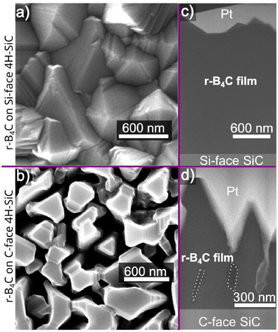
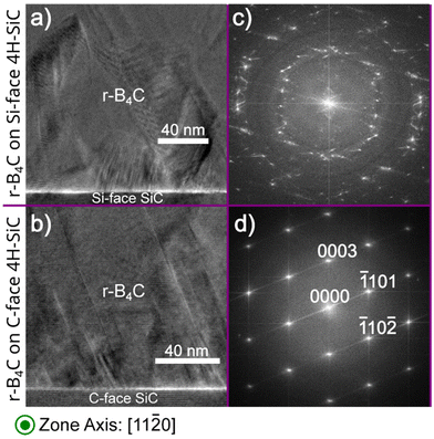
From the previous study, we established that crystalline r-B4C grows on both the C-face and Si-face of 4H-SiC. The r-B4C film grown on the Si-face has a faceted surface morphology (Fig. 1a), while the surface morphology of the film grown on the C-face appears to consist of individual columns separated by voids (Fig. 1b). The cross-section in Fig. 1c shows a dense film on the Si-face, while the cross-section in Fig. 1d shows discernable voids, emphasized by dotted lines in the figure, that extend almost to the film/substrate interface. The cross-sections show that a thicker film, around 2 μm, grows on the Si-face (Fig. 1c), as compared to a thinner film, around 0.9 μm, grows on the C-face (Fig. 1d).Cross-section HRTEM micrographs and their corresponding FFTs of the films grown on both the Si- and C-faces along the (11![[2 with combining macron]](https://www.rsc.org/images/entities/char_0032_0304.gif) 0) 4H-SiC zone axis of the substrate are shown in Fig. 2. The FFT pattern from the r-B4C film on the C-face in Fig. 2 reveals discrete diffraction spots that agree with the XRD results21 confirming the epitaxial relationship with the underlying substrate as r-B4C(0001)[10
0) 4H-SiC zone axis of the substrate are shown in Fig. 2. The FFT pattern from the r-B4C film on the C-face in Fig. 2 reveals discrete diffraction spots that agree with the XRD results21 confirming the epitaxial relationship with the underlying substrate as r-B4C(0001)[10![[1 with combining macron]](https://www.rsc.org/images/entities/char_0031_0304.gif) 0]∥4H-SiC(000
0]∥4H-SiC(000![[1 with combining macron]](https://www.rsc.org/images/entities/char_0031_0304.gif) )[10
)[10![[1 with combining macron]](https://www.rsc.org/images/entities/char_0031_0304.gif) 0]. Line defects extending from the film/substrate interface at an approximate angle of 60° can be seen in Fig. 2b. FFT analysis on the film confirmed that the stacking is the same on either side of the line defect as shown in Fig. S1 in the ESI.† A ring-like FFT pattern consistent with polycrystalline growth is seen for the film growth on Si-face substrates in Fig. 2a. Cross-section HRTEM micrographs and their corresponding FFTs of the films grown on both the Si- and C-faces along (1
0]. Line defects extending from the film/substrate interface at an approximate angle of 60° can be seen in Fig. 2b. FFT analysis on the film confirmed that the stacking is the same on either side of the line defect as shown in Fig. S1 in the ESI.† A ring-like FFT pattern consistent with polycrystalline growth is seen for the film growth on Si-face substrates in Fig. 2a. Cross-section HRTEM micrographs and their corresponding FFTs of the films grown on both the Si- and C-faces along (1![[1 with combining macron]](https://www.rsc.org/images/entities/char_0031_0304.gif) 00) 4H-SiC zone axis of the substrate are shown in Fig. S2 in the ESI.†
00) 4H-SiC zone axis of the substrate are shown in Fig. S2 in the ESI.†
Localized FFT analysis of the epitaxially grown r-B4C on the C-face shows the twinning25,26 of the r-B4C crystal, evidenced by the mirrored FFT pattern observed in Region I and Region II with respect to each other, the FFTs are taken from the marked regions in the HRTEM micrograph as indicated in Fig. 3. The two stackings merge in Region III of Fig. 3, which is supported by the superposition of FFT reflection spots. The additional reflections observed in the FFT from Region III are forbidden but occur due to stacking faults formed during the coalescence of twinned r-B4C crystals.27 FFT of the entire film region in the micrograph has been labeled as Region IV, with reflection spots similar, or identical, to those seen in Region III. Dashed lines in the HRTEM micrograph are used to show the grain boundary as the film grows in the pyramidal triangular microstructure, this growth microstructure starts already at the film/substrate interface. A localized FFT analysis of the r-B4C film grown on the Si-face of 4H-SiC is presented in Fig. S3 in the ESI,† showing several crystallites in the HRTEM micrograph and an overall FFT where the diffraction spots indicate a polycrystalline film.
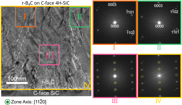 | ||
Fig. 3 Cross-section TEM micrograph of the epitaxially grown r-B4C film on C-face 4H-SiC as observed along the (11![[2 with combining macron]](https://www.rsc.org/images/entities/char_0032_0304.gif) 0) zone axis of the substrate. FFTs of selected areas as well as of the whole micrograph are marked as I–IV on the micrograph. Regions I and II show two crystal stackings twinned relative each other. Region III is the region where the twinned stacking structure merges. The obtained FFT contains diffraction spots from both Regions I and II, but also additional diffraction, marked with dotted yellow circles, as forbidden reflections are present in the FFT. FFT from the whole micrograph is labelled as Region IV. Dashed lines in the HRTEM micrograph are guides for the eyes to show the grain boundary as the film grows in the pyramidal triangular microstructure as seen in Fig. 1. 0) zone axis of the substrate. FFTs of selected areas as well as of the whole micrograph are marked as I–IV on the micrograph. Regions I and II show two crystal stackings twinned relative each other. Region III is the region where the twinned stacking structure merges. The obtained FFT contains diffraction spots from both Regions I and II, but also additional diffraction, marked with dotted yellow circles, as forbidden reflections are present in the FFT. FFT from the whole micrograph is labelled as Region IV. Dashed lines in the HRTEM micrograph are guides for the eyes to show the grain boundary as the film grows in the pyramidal triangular microstructure as seen in Fig. 1. | ||
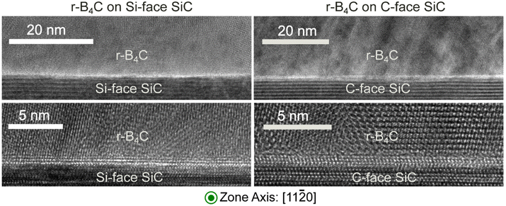
HRTEM images recorded from the film/substrate interfaces are shown in Fig. 4. No difference in interface roughness is noted between the Si- and C-faces, suggesting that surface etching and step bunching of the substrates do not affect crystal stacking between the two substrate surfaces. No indication of graphene or graphite formation is observed, even at the highest magnification.
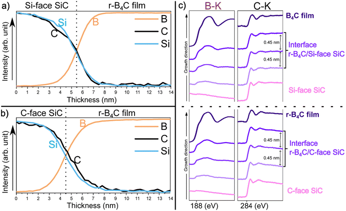
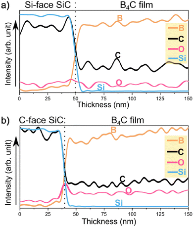
The elemental composition of the film/substrate interface was investigated by EELS line profiles and stacked EELS spectra in Fig. 5. The analysis reveals that the first few nanometer r-B4C film grown on the C-face is higher in carbon content compared to the r-B4C film on the Si-face. The stacked EELS spectra show that similar chemical environments and bonding states are present for B–K and C–K edge spectra at the apparent film/substrate interfaces on both substrates. This suggests that the higher carbon content on the C-face interface does not result in the formation of free carbon or graphene/graphite layers which would influence a difference in epitaxial growth conditions of B4C between the two substrate surfaces. EDX depth profiles taken across the film/substrate interface for r-B4C grown on the Si-face Fig. 6(a) and C-face in Fig. 6(b), show the oxygen contributions in the elemental composition. As can be seen, there is an increase in oxygen signal starting from the film nucleation r-B4C film grown on the C-face, while it remains at the base level (same as in the substrate) for the film growing on the Si-face.
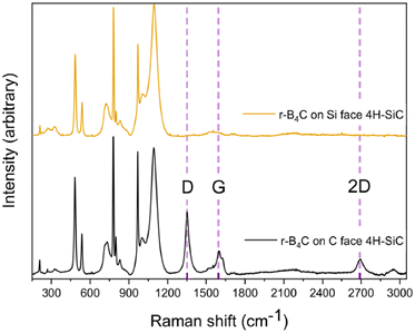
Raman spectroscopy reveals the presence of free carbon on the surface of the epitaxial film, as shown in Fig. 7. The characteristic D, G, and 2D bands of carbon are observed, at 1352 cm−1, 1595 cm−1, and 2690 cm−1 respectively, only on the epitaxial r-B4C films grown on the C-face. In contrast, the polycrystalline r-B4C films grown on the Si-face show no peaks from free carbon.
Discussion
The outstanding question from our previous study21 is why r-B4C grows epitaxially on the C-face but not on the Si-face. From that study and the results presented here, we conclude that r-B4C nucleates and grows on both faces of 4H-SiC, but on the C-face, it grows epitaxially and grows to less than half the thickness compared to the polycrystalline r-B4C film growth on the Si-face. The surface morphologies are accordingly different for the two 4H-SiC faces (Fig. 1). HRTEM in Fig. 4 and stacked-EELS spectra in Fig. 5c results reveal that these differences cannot be explained by SiC surface roughness (Fig. 4) or from the presence of interlayers (Fig. 4 and 5c). It should be noted that the epitaxial r-B4C film on the C-face and the polycrystalline film on the Si-face (Fig. 1) were both grown in the same CVD experiment.Higher carbon content is observed in the first few nanometers of the r-B4C film on the C-face compared to the Si-face (Fig. 5a and b). Given that r-B4C grew epitaxially on the C-face, we could reason that this initial carbon in the film may be important for the initial stages of epitaxial growth of r-B4C films on 4H-SiC. The B atoms in B4C form caged structures which leads to the characteristic network of boron icosahedra seen in boron carbide.28 The suggested role of carbon is to stabilize this network by supplying electrons to the boron icosahedron.29 However, these considerations rely heavily on the experimental results from the EELS analysis alone and the supporting reasoning is highly speculative. This could also be a consequence of epitaxial growth and not necessarily the reason for it.
We also observe an increase in the oxygen signal starting from film nucleation from the EDX depth profiles of the r-B4C that grew epitaxially on the C-face. However, this difference could be a consequence of the epitaxial film's microstructure and the presence of voids (Fig. 1). ERDA depth profiles for these films in the previous study showed 0.3% and 0.1 at% of O for the film grown on the C-face and the Si-face respectively.21 The difference is marginal from the ERDA analysis where the analyzed film is intact during measurements as opposed to the TEM sample preparation process done before the EDX analysis, as required. It is hard to differentiate between the oxygen incorporation during and after deposition, making this result less reliable.
The difference in film thickness could be explained by a hampered growth process on the C-face. From our work on epitaxial growth of hexagonal and rhombohedral boron nitride (h-BN and r-BN) by CVD using TEB where we also observe similarly shaped pyramid structures, we have noted that the epitaxial growth is hampered by surface poisoning from carbon species.30 We therefore use Raman spectroscopy (Fig. 7) to search for signs of carbon surface poisoning on the r-B4C films. This analysis reveals free carbon on the surface of the r-B4C films grown only for the C-face. We suggest that carbon accumulation on the growth surface hampers the growth of epitaxial r-B4C films. The polycrystalline r-B4C grown on the Si-face is continuous. We speculate that the absence of surface carbon on the film grown on the Si-face (Fig. 7) is due to the surface morphology of that film where the highly faceted surface allows migration and subsequent desorption of hydrocarbon species. The difference in film thickness can also be attributed to a faster polycrystalline film growth rate, as explained by a competitive growth mode.31 Competitive growth mode is often encountered in thin film growth and is where the dominant growth of crystallites is determined by the fastest-growing crystal facets. In contrast, epitaxial growth occurs only in one crystal orientation. In addition, Raman spectroscopy shows that carbon accumulates on the surface of the epitaxial r-B4C films. Thus, the resulting difference in film thickness could be a combination of carbon accumulation and the difference in growth modes. Our result suggests that a growth chemistry that is more capable of removing carbon is necessary for epitaxial r-B4C film growth in this process. These experimental results cannot explain why r-B4C grows epitaxially on the C-face and polycrystalline on the Si-face. We speculate that the atomistic understanding of this is likely in the initial chemical bonds formed between the surface atoms and the r-B4C and hope that these results spur interest to model the interface by quantum chemical modelling.
Conclusion
Our study shows that the epitaxial growth of rhombohedral boron carbide, r-B4C films on the (000![[1 with combining macron]](https://www.rsc.org/images/entities/char_0031_0304.gif) ) surface, but not on the (0001) surface of 4H-SiC is not due to interface roughening or formation of any interlayer. We cannot give a detailed atomistic explanation for the differences in the growth modes, but the experimental results develop the knowledge on the r-B4C/4H-SiC interface, the epitaxial r-B4C film and its growth morphology. We argue that epitaxial r-B4C film growth is hindered by carbon accumulation and poisoning of the growing surface.
) surface, but not on the (0001) surface of 4H-SiC is not due to interface roughening or formation of any interlayer. We cannot give a detailed atomistic explanation for the differences in the growth modes, but the experimental results develop the knowledge on the r-B4C/4H-SiC interface, the epitaxial r-B4C film and its growth morphology. We argue that epitaxial r-B4C film growth is hindered by carbon accumulation and poisoning of the growing surface.
Conflicts of interest
There are no conflicts to declare.Acknowledgements
This work was supported by the Swedish Research Council (VR) under contracts; No. 2017-04164 and No. 2018-05499. H. H. and H. P. acknowledge the Swedish Government Strategic Research Area in Materials Science on Functional Materials at Linköping University (Faculty Grant SFO-Mat-LiU No. 2009-00971). Swedish Research Council and Swedish Foundation for Strategic Research for access to ARTEMI, the Swedish National Infrastructure in Advanced Electron Microscopy (2021-00171 and RIF21-0026). I. G. I. acknowledges support from the Knut and Alice Wallenberg Foundation (Grant No. KAW 2018.0071).References
- R. Kuliiev, Mechanical Properties of Boron Carbide, J. Am. Ceram. Soc., 1984, 67(1), C-13–C-14 Search PubMed.
- S. G. Savio, K. Ramanjaneyulu, V. Madhu and T. B. Bhat, An Experimental Study on Ballistic Performance of Boron Carbide Tiles, Int. J. Impact Eng., 2011, 38(7), 535–541, DOI:10.1016/j.ijimpeng.2011.01.006.
- K. Madhav Reddy, J. J. Guo, Y. Shinoda, T. Fujita, A. Hirata, J. P. Singh, J. W. McCauley and M. W. Chen, Enhanced Mechanical Properties of Nanocrystalline Boron Carbide by Nanoporosity and Interface Phases, Nat. Commun., 2012, 3, 1052, DOI:10.1038/ncomms2047.
- J. Chen, Y. Zeng, X. Liang, Y. Hou, Y. Wang, Z. Sun and S. Cui, Lightweight Design and Experimental Study of Ceramic Composite Armor, Processes, 2022, 10(6), 1056, DOI:10.3390/pr10061056.
- D. Emin and T. L. Aselage, A Proposed Boron-Carbide-Based Solid-State Neutron Detector, J. Appl. Phys., 2005, 97(1), 013529, DOI:10.1063/1.1823579.
- A. D. Harken, E. E. Day, B. W. Robertson and S. Adenwalla, Boron-Rich Semiconducting Boron Carbide Neutron Detector, Jpn. J. Appl. Phys., Part 1, 2005, 44(1 A), 444–445, DOI:10.1143/JJAP.44.444.
- Y. Ben-Galim, U. Wengrowicz, A. Raveh and I. Orion, Gamma Scintillator System Using Boron Carbide for Neutron Detection, Nucl. Instrum. Methods Phys. Res., Sect. A, 2014, 756, 62–67, DOI:10.1016/j.nima.2014.04.022.
- G. Nowak, M. Störmer, H. W. Becker, C. Horstmann, R. Kampmann, D. Höche, M. Haese-Seiller, J. F. Moulin, M. Pomm, C. Randau, U. Lorenz, R. Hall-Wilton, M. Müller and A. Schreyer, Boron Carbide Coatings for Neutron Detection Probed by X-Rays, Ions, and Neutrons to Determine Thin Film Quality, J. Appl. Phys., 2015, 117(3), 034901, DOI:10.1063/1.4905716.
- J. Zhu, Y. Liu, J. Zhou, Z. Yang, H. Zhu, X. Zhou, J. Tan, M. Cui and Z. Sun, Structural and Component Characterization of the B4C Neutron Conversion Layer Deposited by Magnetron Sputtering, Nucl. Eng. Technol., 2023, 55(9), 3121–3125, DOI:10.1016/j.net.2023.05.013.
- H. Werheit, H. Binnenbruck and A. Hausen, Optical Properties of Boron Carbide and Comparison with B–rhombohedral Boron, Phys. Status Solidi, 1971, 47(1), 153–158, DOI:10.1002/pssb.2220470118.
- H. Werheit, M. Laux, U. Kuhlmann and R. Telle, Optical Interband Transitions of Boron Carbide, Phys. Status Solidi, 1992, 172(2), K81–K86, DOI:10.1002/pssb.2221720233.
- H. V. Saritha Devi, M. S. Swapna, G. Ambadas and S. Sankararaman, Optical Emission Diagnosis of Boron Carbide Synthesized Using Natural Carbon Precursors, Opt. Spectrosc., 2018, 125(6), 928–932, DOI:10.1134/S0030400X18120251.
- A. Bute, S. Jena, R. K. Sharma, Jagannath, D. V. Udupa and N. Maiti, Linear and Non-Linear Optical Properties of Boron Carbide Thin Films, Appl. Surf. Sci., 2023, 608, 155101, DOI:10.1016/j.apsusc.2022.155101.
- M. Bouchacourt and F. Thevenot, The Correlation between the Thermoelectric Properties and Stoichiometry in the Boron Carbide Phase B4C-B10.5C, J. Mater. Sci., 1985, 20(4), 1237–1247, DOI:10.1007/BF01026319.
- S. Sasaki, M. Takeda, K. Yokoyama, T. Miura, T. Suzuki, H. Suematsu, W. Jiang and K. Yatsui, Thermoelectric Properties of Boron-Carbide Thin Film and Thin Film Based Thermoelectric Device Fabricated by Intense-Pulsed Ion Beam Evaporation, Sci. Technol. Adv. Mater., 2005, 6(2), 181–184, DOI:10.1016/j.stam.2004.11.010.
- H. Werheit, Thermoelectric Properties of Boron-Rich Solids and Their Possibilities of Technical Application, Int. Conf. Thermoelectr. ICT, Proc., 2006, pp. 159–163. DOI:10.1109/ICT.2006.331323.
- P. Sauerschnig, J. L. Watts, J. B. Vaney, P. C. Talbot, J. A. Alarco, I. D. R. Mackinnon and T. Mori, Thermoelectric Properties of Phase Pure Boron Carbide Prepared by a Solution-Based Method, Adv. Appl. Ceram., 2020, 119(2), 97–106, DOI:10.1080/17436753.2019.1705017.
- K. Saglik, B. Mete, I. Terzi, C. Candolfi and U. Aydemir, Thermoelectric Borides: Review and Future Perspectives, Adv. Phys. Res., 2023, 2(8), 2300010, DOI:10.1002/apxr.202300010.
- M. Bouchacourt and F. Thevenot, The Melting of Boron Carbide and the Homogeneity Range of the Boron Carbide Phase, J. Less-Common Met., 1979, 67(2), 327–331, DOI:10.1016/0022-5088(79)90007-9.
- F. Thévenot, Boron Carbide-A Comprehensive Review, J. Eur. Ceram. Soc., 1990, 6(4), 205–225, DOI:10.1016/0955-2219(90)90048-K.
- L. Souqui, S. Sharma, H. Högberg and H. Pedersen, Texture Evolution in Rhombohedral Boron Carbide Films Grown on 4H-SiC(000
![[1 with combining macron]](https://www.rsc.org/images/entities/char_0031_0304.gif) ) and 4H-SiC(0001) Substrates by Chemical Vapor Deposition†, Dalton Trans., 2022, 51, 15974–15982, 10.1039/d2dt02107b.
) and 4H-SiC(0001) Substrates by Chemical Vapor Deposition†, Dalton Trans., 2022, 51, 15974–15982, 10.1039/d2dt02107b. - Y. Benamra, L. Auvray, J. Andrieux, F. Cauwet, M. P. Alegre, L. Lloret, D. Araujo, M. Gutierrez and G. Ferro, Epitaxial Growth of Boron Carbide on 4H-SiC, Solid State Phenom., 2023, 343(0001), 3–8, DOI:10.4028/p-6t47nz.
- W. Norimatsu, K. Matsuda, T. O. Terasawa, N. Takata, A. Masumori, K. Ito, K. Oda, T. Ito, A. Endo, R. Funahashi and M. Kusunoki, Controlled Growth of Boron-Doped Epitaxial Graphene by Thermal Decomposition of a B4C Thin Film, Nanotechnology, 2020, 31, 145711, DOI:10.1088/1361-6528/ab62cf.
- C. L. Jia, M. Lentzen and K. Urban, High-Resolution Transmission Electron Microscopy Using Negative Spherical Aberration, Microsc. Microanal., 2004, 10(2), 174–184, DOI:10.1017/S1431927604040425.
- B. Wei, R. Vajtai, Y. J. Jung, F. Banhart, G. Ramanath and P. M. Ajayan, Massive Icosahedral Boron Carbide Crystals, J. Phys. Chem. B, 2002, 106(23), 5807–5809, DOI:10.1021/jp014640f.
- M. Imam, L. Souqui, J. Herritsch, A. Stegmüller, C. Höglund, S. Schmidt, R. Hall-Wilton, H. Högberg, J. Birch, R. Tonner and H. Pedersen, Gas Phase Chemistry of Trimethylboron in Thermal Chemical Vapor Deposition, J. Phys. Chem. C, 2017, 121(47), 26465–26471, DOI:10.1021/acs.jpcc.7b09538.
- H. Z. Xiao and A. C. Daykin, Extra Diffractions Caused by Stacking Faults in Cubic Crystals, Ultramicroscopy, 1994, 53(4), 325–331, DOI:10.1016/0304-3991(94)90045-0.
- V. Domnich, S. Reynaud, R. A. Haber and M. Chhowalla, Boron Carbide: Structure, Properties, and Stability under Stress, J. Am. Ceram. Soc., 2011, 94(11), 3605–3628, DOI:10.1111/j.1551-2916.2011.04865.x.
- M. M. Balakrishnarajan, P. D. Pancharatna and R. Hoffmann, Structure and Bonding in Boron Carbide: The Invincibility of Imperfections, New J. Chem., 2007, 31(4), 473–485, 10.1039/b618493f.
- S. Sharma, J. Palisaitis, I. G. Ivanov, O.Å Persson, H. Pedersen and H. Högberg, The Influence of Carbon on Polytype and Growth Stability of Epitaxial Hexagonal Boron Nitride Films and Layers, Adv. Mater. interfaces, 2024, 2400091, DOI:10.1002/admi.202400091.
- G. Carter, Preferred Orientation in Thin Film Growth - the Survival of the Fastest Model, Vacuum, 2000, 56(2), 87–93, DOI:10.1016/S0042-207X(99)00171-2.
Footnotes |
| † Electronic supplementary information (ESI) available. See DOI: https://doi.org/10.1039/d4dt01157k |
| ‡ Present address: Department of Materials Science and Engineering, University of Illinois at Urbana-Champaign, 1304W. Green St. MC 246, Urbana, Illinois 61801, USA. |
| This journal is © The Royal Society of Chemistry 2024 |

