
Resistance switching of graphene by gate-controlled polarization reorientation of polyvinylidene fluoride in a field effect transistor†
Jinhee
Lee
ab,
Nodo
Lee
bc,
Yves
Lansac
 abde and
Yun Hee
Jang
*abde
abde and
Yun Hee
Jang
*abde
aDepartment of Energy Science and Engineering, DGIST, Daegu 42988, Korea. E-mail: yhjang@dgist.ac.kr
bSchool of Materials Science and Engineering, GIST, Gwangju 61005, Korea
cMaterials & Devices Research Institute, LG Electronics, Seoul 07796, Korea
dGREMAN, UMR 7347, CNRS, Université de Tours, 37200 Tours, France
eLPS, UMR 8502, CNRS, Université Paris-Saclay, 91405 Orsay, France
First published on 6th September 2024
Abstract
Ferroelectric β-phase crystals of a polyvinylidene fluoride (PVDF) polymer grown or deposited on a graphene channel of a field effect transistor would induce various degrees of electrostatic doping (i.e., various amounts of charge carriers) into graphene and in turn ON/OFF switching of the device, only if the electric field applied at the gate can reorient its polarization (i.e., the well-aligned F-to-H dipole moments perpendicular to the all-trans polymer backbone) around the polymer backbone. To assess the feasibility of achieving a β-PVDF/graphene ferroelectric field effect transistor or memory device, we mimic (1) the electric-field-controlled PVDF polarization reversal (with density functional theory calculations and molecular dynamics simulations) and (2) the conductance switching of β-PVDF/graphene by PVDF reorientations (F-, H- and FH-down) representing a cycle of gate-voltage sweep (with density functional theory combined with non-equilibrium Green's function formalism). The low energy barrier of the collective synchronous PVDF chain rotation around the backbone (0.22 eV per monomer) and the high electric field required to initiate the chain rotation (16 V nm−1) are compatible with the domain nucleation-growth theory and would support the polarization-induced resistance switching mechanism if the PVDF film is ultrathin and partially amorphous.
Introduction
Graphene with high carrier mobility can replace the current silicon-based electronic materials,1 but doping is necessary due to the high resistance of undoped graphene near the Dirac point.2,3 Applying electric (E) field to shift the Fermi energy from the Dirac point can be a non-destructive way of doping (Fig. 1a)4–6 since the mobility is high even under high E-fields.2 However, retaining such doped states requires continuous E-field application and thus high-energy consumption.3 Alternatively, ions7,8 or polarized dipoles of a ferroelectric layer can dope graphene even under zero E-field (Fig. 1b). Low-power-consuming post-silicon electronic devices such as synapse-mimicking field-effect transistors,3,7,9–17 memories,18–20 and electrodes4,21–24 have been realized by such electrostatic doping of graphene (or other semiconducting channels) with ferroelectric layers.2,5,6 Polyvinylidene fluoride (PVDF; [C2F2H2]n and its copolymers, Fig. 1c) is a ferroelectric polymer that is the most widely used as such a gate dielectric layer.25–27 PVDF shows lower remnant polarizations than its inorganic counterparts such as lead zirconate titanate (PZT; PbZr1−xTixO3)19,28 but has various merits such as low crystallization temperature,29,30 flexibility,31 non-toxicity, and low concentration of surface charge traps.32 Among its various polymorphs, the β-phase crystal has the maximum spontaneous polarization,33 which originates from the well-aligned F-to-H dipole moments across the all-trans C backbone (Fig. 1c). Such a polarization can shift the Fermi energy of graphene with respect to the Dirac point and in turn adjust the electrostatic doping level6 (Fig. 1a) and the ON/OFF (or low/high-resistance) states of the graphene channel. | ||
| Fig. 1 (a) Partial density of states (DOS) of graphene and the Fermi levels of (b) β-PVDF/graphene interface models built in three major configurations, i.e., F-down and H-down configurations built with a 5-layer (110) slab and the FH-down configuration built with a 5-layer (100) slab, which are cut from (c) the β-PVDF crystal [H (black), C (grey), and F (green)]. The (110) and (100) planes (top and bottom in c; orange), the polarization (dipole moment) directions (red-to-blue arrows in b and c), and the layer-by-layer (0 = graphene; 1–5 = PVDF) Bader charges (red, grey, and blue curves in (b); see Methods and models below) are shown together. | ||
Our previous molecular dynamics (MD) simulations and density functional theory (DFT) calculations34,35 have mimicked in silico the amorphous-to-β-phase PVDF crystallization induced by shear stress (spin coating) and the shift of the electronic energy levels (i.e., DOS) and the doping of graphene induced at three major polarization orientations (F-down, H-down, and FH-down) of the β-PVDF layer (Fig. 1). Indeed, the F- and H-down orientations induce oppositely signed slightly asymmetric doping into graphene (PF-down ≥ − PH-down)4,13 and the FH-down orientation induced negligible doping (PFH-down ≈ 0).9,23
Such a bi-stable switching operation would be possible only if the polarization reorientation or reversal is controlled by E-fields applied on the β-PVDF/graphene device during the gate voltage sweeps. However, the polarization reversal itself (i.e., PVDF chain rotation around its backbone) has not been observed nor simulated at the molecular level. Most of the theoretical studies focus on the energy barrier of chain rotation36,37 rather than E-field-induced spontaneous rotation. There have been only a few studies on the polarization switching dynamics of PVDF chains under E-fields.38,39 The speculated mechanism that the initial rate-determining step (nucleus generation) is followed by the prompt domain propagation or growth40 has been borrowed from the mechanism for its inorganic counterparts.41–43
Therefore, herein we mimic in silico the E-field-controlled PVDF polarization reversal (chain rotation) by MD simulations at various E-field strengths. Above a critical E-field strength, we find that a seed or a nucleus generated in the initial stage leads very fast to a complete polarization reversal. The energy barrier for the initial nucleation is estimated. The energy barrier for collective synchronous rotations of PVDF is also calculated using the climbing-image-nudged-elastic-band (CI-NEB) DFT method.44,45 Our estimations are compatible with the domain nucleation-growth mechanism. Then, the charge transport through graphene doped with the three major polarization orientations (F-, H- and FH-down) of β-PVDF is calculated by DFT combined with a non-equilibrium Green's function theory (NEGF) to mimic the ON/OFF (low/high resistance) switching in the polarization hysteresis loop.
Methods and models
CI-NEB DFT (PVDF bulk unit cell)
It is known that, once formed via spin coating and poling, the β phase is retained.46 We thus focus on the β-phase PVDF. First, the energy barrier of the chain rotation about the backbone aligned in the z axis is estimated by the CI-NEB DFT calculation on the smallest unit cell of the β-PVDF crystal, which contains two polymer chains per unit cell and a single monomer unit (C2F2H2 or a single dipole moment) in the z direction (Fig. 1c). The chain rotation is represented by a series of 11 intermediate states (i.e., images) between the initial state with the fully relaxed β-PVDF (8.31 × 4.67 × 2.58 Å3; 7% error from the experimental structure33) and the final state where both chains are rotated by 180°. They are generated by rotating both chains together by 15° while conserving the intrachain geometries (bonds, angles, and torsions). At each state, a plane-wave spin-unpolarized DFT calculation is carried out using the Perdew–Burke–Ernzerhof (PBE) functional47,48 and the previously-validated34,49 D3 dispersion correction of Grimme50 implemented in the VASP.51 The core electrons are replaced by the projector-augmented-wave pseudo-potentials, while the valence electrons are represented by plane-waves with kinetic energies up to 600 eV. A Monkhorst–Pack k-point mesh of 3 × 6 × 12 is used for the Brillouin zone sampling. The convergence criterion is 1 × 10⁻⁵ eV for the electronic structure and 1 × 10⁻⁴ eV for full relaxation of atomic positions until the Hellmann–Feynman forces converge to less than 0.01 eV Å−1.MD with E-field (PVDF bulk supercell)
To grasp the early-stage response of the β-phase PVDF to E-field, which has been elusive experimentally, we carry out MD simulations on larger-scale models of the β-PVDF crystal under various strengths of E-fields. The β-phase PVDF crystal is represented by its 3 × 9 × n supercells (1 ≤ n ≤ 12). These 12 supercells gradually expanded in the chain-axis direction ([001] or z) are employed to confirm the convergence with the chain length in a unit cell. The lattice parameters of the largest 3888-atom 648-monomer-unit supercell considered (n = 12) are 2.61 × 4.18 × 2.99 nm3. The E-field is applied along the [010] or y direction opposite to the initial polarization direction (i.e., perpendicular to the polymer backbone) with its strength increased from 10 to 20 GV m−1 (=V nm−1) by an increment of 0.2 GV m−1 to determine the critical E-field (Ec) or the minimum E-field required for any chain flip. Stronger E-fields than those used in previous studies52 are used to accelerate the process.53–55 At each E-field, the supercell is equilibrated at 298 K for 1 ns by NVT MD simulation with the Nose–Hoover thermostat56 implemented in the Materials Studio (BIOVIA). We use the MSXX force field of Karasawa and Goddard III,57 which has been validated in our previous studies.34,35 The applied E-field (E) exerts additional force (F = q E) on each atom, which is proportional to the atom charge (q; CH −0.54, H 0.18, CF 0.70, and F −0.26 |e|),57 and rotates the dipole moments of PVDF chains to align parallel to the E-field. The rotation energy barrier per C2H2F2 monomer unit is given as the critical E-field Ec (V m−1) multiplied by the average dipole moment μ (C m) per monomer unit.NEGF DFT (β-PVDF/graphene)
To prepare the β-PVDF/graphene interface models, the hexagonal unit cell of single-layer graphene is first redefined to an orthorhombic unit cell. Then, the β-phase crystal of PVDF is cleaved along the (110) direction into 5-layer F-down and H-down PVDF films and along the (100) direction into a 5-layer FH-down PVDF film (Fig. 1c). A vacuum slab of 15 Å in the y direction is inserted on top of these β-PVDF/graphene composites composed of 34 atoms (four C atoms of graphene and five C2F2H2 units, Fig. 1b). To resolve lattice mismatch between graphene and β-PVDF in the x direction, the interchain distance is adjusted by −12% and 3.7% in the (110) and (100) films, respectively. The optimum interlayer distance in the y direction between graphene and the bottommost atoms of H-down, F-down, and FH-down PVDF is determined to be 2.4, 2.9, and 3.1 Å, respectively, from a series of single-point energy calculations at different distances followed by atom-position relaxations around the minimum-energy distance (Fig. 2a). The 9 × 1 × 15 and 27 × 1 × 45 Monkhorst–Pack k-point meshes are used for geometry optimization and for DOS and Bader atom charge58–60 analyses (Fig. 1), respectively.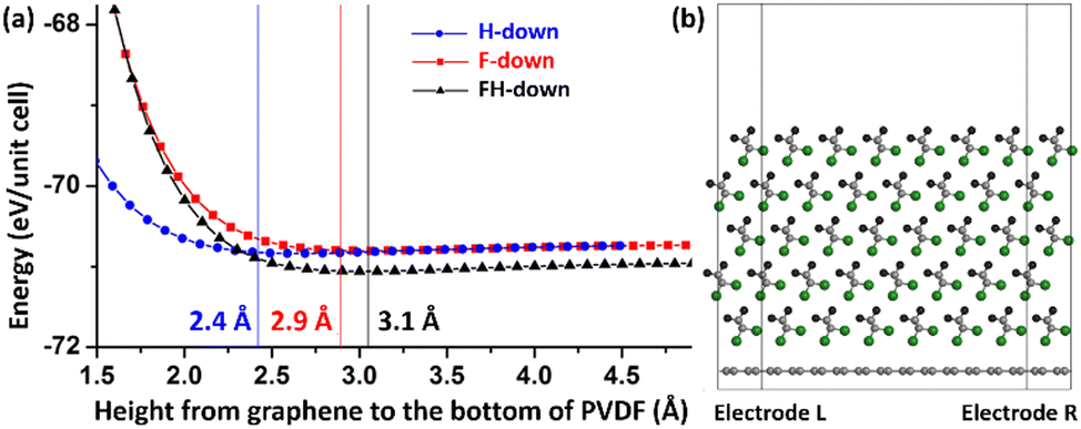 | ||
| Fig. 2 (a) Total energy (eV) per 34-atom unit cell of three β-PVDF/graphene models (H-down, F-down, and FH-down; Fig. 1b) and their minimum-energy heights from graphene to the bottommost atoms of PVDF. (b) The 8 × 1 × 1 supercell of the optimized model (F-down as an example) built as a two-probe device model to calculate tunnelling currents (I) through graphene doped with PVDF at bias voltages (V) applied to the two electrodes. | ||
The 8 × 1 × 1 supercells of these optimized structures are used as models for two-probe β-PVDF/graphene devices composed of left and right electrodes and the central region (Fig. 2b). The quantum transport (i.e., tunnelling current I) through the graphene doped with PVDF chains in each polarization orientation is calculated at each bias voltage (V) applied to the two electrodes with the DFT-NEGF formalism, the PBE functional, and the localized double-ζ polarized (DZP) basis set implemented in the QuantumATK code.61–64 The external bias voltage V is increased from 0 to 0.2 V by 0.025 V. The mesh cut-off energy for real space grid density is 150 Ry. The k-points of 20 × 1 × 40 and 2 × 1 × 40 are used for each electrode and the central region, respectively, for the self-consistent field cycles. The current I at each V is estimated by integrating the transmission T(E,V) over the bias window of E between −eV/2 and eV/2 using the Landauer–Büttiker formula,65

Results and discussion
CI-NEB DFT (energy barrier for collective rotation)
Fig. 3 shows that, due to the crystal symmetry, only one sixth of the considered images, 0° (the equilibrium state) to 30° (the transition state), are unique. The activation energy barrier to climb up from 0° to 30° is calculated to be 0.44 eV per unit cell, i.e., 0.22 eV per C2F2H2 monomer (or single dipole) unit. This is close to the value (0.16 eV per C2F2H2) previously estimated for synchronous rotation of all the seven chains in a hexagonal PVDF bundle.36 However, it is much lower than the barrier (0.84 eV per C2F2H2) calculated for the rotation of the central chain against the six other antiparallel neighbours.36 It implies that a collective synchronous rotation of all the PVDF chains over the entire phase is easier than an antiparallel seed generation by a single-chain rotation. It also implies that the initial single-molecule rotation (seed formation or domain nucleation) is the rate determining step which requires a much higher energy than that required for the collective synchronous rotation (domain growth or propagation). Thus, once the initial seed generation is realized, the collective synchronous polarization reversal would follow it fast. | ||
| Fig. 3 Energy barrier (eV) per unit cell (containing two C2F2H2 monomer units) of a collective synchronous chain rotation around the backbone in the β-phase PVDF crystal, which is estimated by the climbing-image-nudged-elastic-band (CI-NEB) DFT calculations. | ||
MD under E-field (critical E-field and nucleation energy barrier)
Then, what would be the early-stage response of the β-phase PVDF to the E-field of a sufficient energy, i.e., the critical E-field Ec? Would it be an avalanche-type collective synchronous rotation of all the PVDF chains or a single-chain rotation (domain nucleation) followed by its propagation (domain growth)?Irrespective of the model size n, all our simulations show that, when the critical E-field Ec is reached, a single chain of PVDF first flips over (seed generation; Fig. 4a, red circle), climbing over the energy barrier exerted by the neighbouring antiparallel chains, and then the neighbouring chains flip over subsequently and finally complete the polarization reversal (domain growth) quickly within 3 ps, as shown in the abrupt time evolution of the y component of polarization (Fig. 4b, red). Thus, the polarization reversal of β-PVDF can be described as a seed (nucleus) formation at Ec followed by an avalanche-type domain expansion.
 | ||
| Fig. 4 (a) and (b) Time evolution of a 3 × 9 × n (n = 9) supercell of the β-phase PVDF and its total polarization (dipole moments) along each direction during MD simulations under the critical E-field (Ec = 16.4 GV m−1) applied opposite to the original polarization aligned in the y direction. The chains flipped during the nucleation and propagation of polarization reversal are marked with red circles. Movies can be found in the ESI.† (c) Nucleation energy barriers (red curve) estimated from the dipole moment per monomer unit and the critical electric field (black curve). Both curves converge quickly to about 16 GV m−1 and about 9 eV per C2H2F2 monomer unit, respectively, with the size n (1, 3, 6, 9, and 12) of the supercell along the polymer backbone. | ||
The Ec value varies with the model size n (Fig. 4c, black curve) but converges quickly to about 16 GV m−1 (=V nm−1) for n ≥ 12. Most of the supplied energy appears to be used for the reversal of the first PVDF chain (nucleus formation), which has been indeed assumed to be the rate-determining step. The energy barrier for this first chain rotation (=Ec × μ) is estimated to be 0.94 eV per C2H2F2 when n is 9, for example, since Ec is estimated to be 16.4 V nm−1 and the average dipole moment μ is estimated to be 5.8 × 10⁻² |e|·nm per C2H2F2 (=1340 D = 4.5 × 10⁻²⁷ C·m = 28 |e|·nm for 486 monomer units). This initial nucleation energy barrier also increases with the model size n and saturates quickly to about 0.9 eV (Fig. 4c, red curve). This energy barrier is indeed close to the energy barrier (0.84 eV per C2F2H2) calculated for the single-chain rotation against antiparallel neighbours.36 This energy barrier is also comparable with slightly lower energy barriers (0.4–0.8 eV)38,39,66 estimated from the domain nucleation-growth models on PVDF and its popular copolymer trifluoroethylene (PVDF-TrFE), which is known to be easier to manipulate than PVDF.
DFT-NEGF (I–V curve of PVDF-doped graphene)
These polarized β-PVDF layers induce p-doping (F-down) and n-doping (H-down) of graphene (Fig. 1a) by shifting its Fermi level from the Dirac point to a lower (F-down) or a higher (H-down) energy level (Fig. 1b) when the polarization orientation is perpendicular to graphene.34 In contrast, the polarization parallel to graphene (FH-down) does not induce such a Fermi level shift or doping (Fig. 1a and b).34 [The calculated doping concentrations (in the unit of 1013 cm−2) are negligible under a single layer of PVDF, increase with the number of PVDF layers, but saturate quickly, i.e., 0.4, 3.9, 6.0, 7.1, and 7.4 (F-down) and 0.2, 2.7, 4.9, 5.9, and 6.1 (H-down) under one to five layers,34 justifying our β-PVDF/graphene models with only five PVDF layers. The Fermi level shift and the doping of graphene under other β-PVDF orientations can be described by interpolation or superposition of these values calculated under the three major orientations.]As expected from the DFT calculations, different resistance states of graphene are identified by the DFT-NEGF calculations at different polarization orientations of β-PVDF (Fig. 5a). The current I along the graphene channel at each source-to-drain bias voltage Vds is slightly higher under the F-down PVDF (red) than under the H-down PVDF (blue), i.e., IF-down/IH-down ≈ 1.2 (120%), due to a small difference in the doping concentration (7.4 × 10¹³ and 6.1 × 1013 cm−2) caused by the strong electronegativity of F (3.98 vs. 2.55 of C and 2.20 of H).34 This asymmetry is consistent with an experimental report on the shift of the charge neutrality point under a poling bias.10 Both currents (IF-down and IH-down) are much higher than the current under the FH-down PVDF (IFH-down, black), i.e., IF-down/IFH-down = 22 (2200%) and IH-down/IFH-down = 19 (1900%).
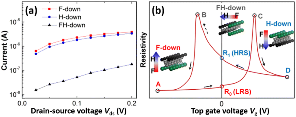 | ||
| Fig. 5 (a) I–V curves at different polarization orientations of PVDF. (b) Conventional resistivity hysteresis loop scheme with different polarization orientations of PVDF. | ||
The switching mechanism of the β-PVDF/graphene type field-effect transistor is typically presented using an electric hysteresis loop (Fig. 5b).17,25–27,40,67 The minimum resistivity is achieved by increasing the gate voltage Vg in two opposite directions. Two low-resistance (ON) states (LRS) with the maximum polarizations, A (F-down) and D (H-down), are created. The slight asymmetry (i.e., the non-unity ratio) between the resistivities of the two oppositely saturated states (D/A ≈ 1.2; Fig. 5a) is again well depicted and confirmed experimentally: 2.5 at ±20 V,13 1.37 at ±40 V,10 and ∼1 at ±80 V.3 Since their polarizations stay as the remnant polarizations even after the gate is turned off for low-power operation (Vg = 0 V), these two states (R0 and R1) can be used as non-volatile switches between low and high resistance states (LRS and HRS; Fig. 5b) despite the extremely small switching ratio (≈1.2).
In fact, the true high-resistance (OFF) states corresponding to the FH-down configurations are B and C (Fig. 5b), which mediate the two LRS states (A and D). The switching ratio involving them would be much higher (e.g., C/A ≈ 20 from our DFT-NEGF calculations, Fig. 5a), and our CI-NEB DFT calculation identifies them as stable minimum-energy states (Fig. 3). However, according to our MD simulations (Fig. 4 and Movies S1 and S2, ESI†), the two LRS states, A and D, are converted to each other in an avalanche-type propagation to the entire phase above the critical E-field without stopping at the intermediate states, B and C. We observe only a complete polarization reversal (between A and D), instead of a controlled polarization reorientation (between A and C). We thus envision that a small fraction of amorphous or defective buffer regions introduced inside the all-trans PVDF chains or between the crystalline β-PVDF domains67–71 may decrease the strong correlation between the all-trans PVDF chains and thus prevent (or slow down) such an avalanche-type polarization reversal. The amorphous regions may be able to stabilize the intermediate zero-polarization OFF states (true HRS) at intermediate gate voltages in addition to the original ON (LRS) states, realizing a ferroelectric field-effect transistor with a high ON/OFF switching ratio. Indeed, the PVDF-TrFE copolymer with such defective TrFE units18 and smaller crystalline domains72 is more popular than PVDF itself.
Conclusions
E-Field is applied during a top gate voltage (Vg) sweep across a ferroelectric β-PVDF film of a β-PVDF/graphene field-effect-transistor model device. It controls the polarization orientation of the all-trans PVDF chains and in turn the conductance of the graphene channel underneath. The nucleation rotation barrier reached by the critical (i.e., minimum) E-field Ec required for a single chain rotation around its backbone is estimated to be 0.9 eV per C2F2H2 monomer unit in our MD simulations. It is much higher than the propagation rotation barrier required for the synchronous rotation of all the PVDF chains (0.2 eV per C2F2H2 monomer unit) estimated by our CI-NEB DFT calculations. Therefore, once a single PVDF chain flips over at Ec as the initial seed formation (domain nucleation), it is followed by an avalanche-type propagation of chain rotation and the polarization reversal is completed very fast (domain expansion). Such behaviours and energies are compatible with the widely accepted domain nucleation-growth mechanism. The energetic feasibility of polarization reorientation supports the polarization-dependent resistive switching in the β-PVDF/graphene ferroelectric field effect transistor. However, the current avalanche-type fast polarization reversal in the perfect β-PVDF crystal allows only a negligible close-to-unity switching ratio (∼1.2) between two asymmetric ON states (F-down and H-down). Utilizing all the three major polarizations (i.e., the OFF state corresponding to FH-down or a mixture of F-down and H-down, in addition to the F-down and H-down ON states) would significantly enhance the switching ratio (∼20). We thus propose to slightly reduce the strong correlation between the all-trans PVDF chains by introducing an amorphous or defective region inside the all-trans PVDF chain or between the crystalline β-PVDF domains as in the popular PVDF-TrFE copolymer.Data availability
The VASP code can be found at https://www.vasp.at and cited as https://www.sciencedirect.com/science/article/pii/0927025696000080. The code for Materials Studio (BIOVIA) can be found at the website https://www.3ds.com/products/biovia/materials-studio. The code for ATK can be found at https://docs.quantumatk.com and cited as https://doi.org/10.1088/1361-648X/ab4007.Conflicts of interest
There are no conflicts to declare.Acknowledgements
This work is supported by the National Research Foundation of Korea (RS-2024-00340218, 2019R1A2C2003118) and DGIST (24KUJoint10). The supercomputing time is supported by the KISTI Grand Challenge Program (KSC-2023-CRE-0255).Notes and references
- F. Schwierz, Nat. Nanotechnol., 2010, 5, 487 CrossRef PubMed.
- A. K. Geim and K. S. Novoselov, Nat. Mater., 2007, 6, 183 CrossRef PubMed.
- Y. Zheng, G.-X. Ni, C.-T. Toh, M.-G. Zeng, S.-T. Chen, K. Yao and B. Özyilmaz, Appl. Phys. Lett., 2009, 94, 163505 CrossRef.
- G.-X. Ni, Y. Zheng, S. Bae, C. Y. Tan, O. Kahya, J. Wu, B. H. Hong, K. Yao and B. Özyilmaz, ACS Nano, 2012, 6, 3935 CrossRef CAS.
- M. J. Allen, V. C. Tung and R. B. Kaner, Chem. Rev., 2009, 110, 132 CrossRef PubMed.
- A. H. Castro Neto, F. Guinea, N. M. R. Peres, K. S. Novoselov and A. K. Geim, Rev. Mod. Phys., 2009, 81, 109 CrossRef CAS.
- S. Oh, J.-H. Lee, S. Seo, H. Choo, D. Lee, J.-I. Cho and J.-H. Park, Adv. Sci., 2022, 9, 2103808 CrossRef CAS.
- S. Guo, Z. Wang, X. Chen, L. Li, J. Li, D. Ji, L. Li and W. Hu, Nano Select, 2022, 3, 20 CrossRef CAS.
- Y. Zheng, G.-X. Ni, C.-T. Toh, C.-Y. Tan, K. Yao and B. Özyilmaz, Phys. Rev. Lett., 2010, 105, 166602 CrossRef PubMed.
- H. J. Hwang, J. H. Yang, Y. G. Lee, C. Cho, C. G. Kang, S. C. Kang, W. Park and B. H. Lee, Nanotechnology, 2013, 24, 175202 CrossRef PubMed.
- H. J. Hwang, J. H. Yang, S. C. Kang, C. Cho, C. G. Kang, Y. G. Lee and B. H. Lee, Microelectron. Eng., 2013, 109, 87 CrossRef.
- S. Jandhyala, G. Mordi, D. Mao, M. W. Ha, M. A. Quevedo-Lopez, B. E. Gnade and J. Kim, Appl. Phys. Lett., 2013, 103, 022903 CrossRef.
- S. Raghavan, I. Stolichnov, N. Setter, J.-S. Heron, M. Tosun and A. Kis, Appl. Phys. Lett., 2012, 100, 023507 CrossRef.
- X. Wang, W. Xie and J.-B. Xu, Adv. Mater., 2014, 26, 5496 CrossRef PubMed.
- Y.-L. Sun, D. Xie, J.-L. Xu, X.-M. Li, C. Zhang, R.-X. Dai, X. Li, X.-J. Meng and H.-W. Zhu, Carbon, 2016, 96, 695 CrossRef.
- Z.-D. Luo, M.-M. Yang, Y. Liu and M. Alexe, Adv. Mater., 2021, 33, 2005620 CrossRef.
- B. H. Lee, J. Y. Lee, A. Kumar and S. Y. Lee, Adv. Electron. Mater., 2022, 8, 2200810 CrossRef.
- T.-W. Chang, Y.-S. Li, N. Matsuhisa and C.-C. Shih, J. Mater. Chem. C, 2022, 10, 13372 RSC.
- P. Heremans, G. H. Gelinck, R. Müller, K.-J. Baeg, D.-Y. Kim and Y.-Y. Noh, Chem. Mater., 2011, 23, 341 CrossRef.
- Z. Hu, M. Tian, B. Nysten and A. M. Jonas, Nat. Mater., 2009, 8, 62 CrossRef CAS.
- K. Kim, S.-H. Bae, C. T. Toh, H. Kim, J. H. Cho, D. Whang, T.-W. Lee, B. Özyilmaz and J.-H. Ahn, ACS Appl. Mater. Interfaces, 2014, 6, 3299 CrossRef CAS.
- S.-H. Bae, O. Kahya, B. K. Sharma, J. Kwon, H. J. Cho, B. Özyilmaz and J.-H. Ahn, ACS Nano, 2013, 7, 3130 CrossRef CAS PubMed.
- M. Zhu, J. Wu, Z. Du, R. Y. Tay, H. Li, B. Ozyilmaz and E. H. T. Teo, Nanoscale, 2015, 7, 14730 RSC.
- D. L. Duong, S. Y. Lee, S. K. Kim and Y. H. Lee, Appl. Phys. Lett., 2015, 106, 243104 CrossRef.
- Y. S. Choi, J. Sung, S. J. Kang, S. H. Cho, I. Hwang, S. K. Hwang, J. Huh, H.-C. Kim, S. Bauer and C. Park, Adv. Funct. Mater., 2013, 23, 1120 CrossRef.
- A. Laudari, J. Barron, A. Pickett and S. Guha, ACS Appl. Mater. Interfaces, 2020, 12, 26757 CrossRef PubMed.
- Q. Zhao, Y. Ren, F. Yang, J. Li, F. Wei, Y. Li, C. Deng, B. Xiao, C. Huang, J. Chen, L. Li and W. Hu, ACS Appl. Mater. Interfaces, 2024, 16, 2573 CrossRef PubMed.
- J. Y. Son, S. Ryu, Y.-C. Park, Y.-T. Lim, Y.-S. Shin, Y.-H. Shin and H. M. Jang, ACS Nano, 2010, 4, 7315 CrossRef PubMed.
- R. Gregorio Jr. and D. S. Borges, Polymer, 2008, 49, 4009 CrossRef.
- S.-Y. Chen and I. W. Chen, J. Am. Ceram. Soc., 1998, 81, 97 CrossRef CAS.
- R. C. G. Naber, C. Tanase, P. W. M. Blom, G. H. Gelinck, A. W. Marsman, F. J. Touwslager, S. Setayesh and D. M. de Leeuw, Nat. Mater., 2005, 4, 243 CrossRef CAS.
- R. C. G. Naber, K. Asadi, P. W. M. Blom, D. M. de Leeuw and B. de Boer, Adv. Mater., 2010, 22, 933 CrossRef CAS PubMed.
- R. Hasegawa, Y. Takahashi, Y. Chatani and H. Tadokoro, Polym. J., 1972, 3, 600 CrossRef CAS.
- N. Lee, J. Lee, T. Ryu, Y. Kim, Y. Lansac and Y. H. Jang, Sci. Adv. Mater., 2014, 6, 2422 CrossRef CAS.
- J. H. Yang, T. Ryu, Y. Lansac, Y. H. Jang and B. H. Lee, Org. Electron., 2016, 28, 67 CrossRef CAS.
- G. Zhu, J. Xu, X. Yan, J. Li, Z. Zeng, M. Shen and L. Zhang, Comput. Mater. Sci., 2006, 37, 512 CrossRef CAS.
- Y.-J. Yu and A. J. H. McGaughey, J. Chem. Phys., 2016, 144, 014901 CrossRef PubMed.
- W. J. Hu, D.-M. Juo, L. You, J. Wang, Y.-C. Chen, Y.-H. Chu and T. Wu, Sci. Rep., 2014, 4, 4772 CrossRef.
- P. Sharma, T. J. Reece, S. Ducharme and A. Gruverman, Nano Lett., 2011, 11, 1970 CrossRef.
- T. Furukawa, Phase Transit., 1989, 18, 143 CrossRef.
- M. Avrami, J. Chem. Phys., 1939, 7, 1103 CrossRef.
- Y. Ishibashi and Y. Takagi, J. Phys. Soc. Jpn., 1971, 31, 506 CrossRef.
- R. Landauer, J. Appl. Phys., 1957, 28, 227 CrossRef.
- G. Henkelman, B. P. Uberuaga and H. Jónsson, J. Chem. Phys., 2000, 113, 9901 CrossRef.
- G. Henkelman and H. Jónsson, J. Chem. Phys., 2000, 113, 9978 CrossRef.
- V. Ranjan, L. Yu, M. B. Nardelli and J. Bernholc, Phys. Rev. Lett., 2007, 99, 047801 CrossRef.
- J. P. Perdew, K. Burke and M. Ernzerhof, Phys. Rev. Lett., 1996, 77, 3865 CrossRef.
- J. P. Perdew, K. Burke and M. Ernzerhof, Phys. Rev. Lett., 1997, 78, 1396 CrossRef.
- F. Xu, X. Chen and N. Wang, J. Polym. Res., 2024, 31, 112 CrossRef.
- S. Grimme, J. Antony, S. Ehrlich and H. Krieg, J. Chem. Phys., 2010, 132, 154104 CrossRef.
- G. Kresse and J. Furthmüller, Comput. Mater. Sci., 1996, 6, 15 CrossRef.
- J. Yang, X. Yao and Z. Meng, Polymer, 2022, 245, 124691 CrossRef PubMed.
- T. Wang, Y. Gao, B. Chen, V. H. Crespi and A. C. T. van Duin, Nano Lett., 2024, 24, 9195 CrossRef.
- K. Chelakara Satyanarayana and K. Bolton, Polymer, 2012, 53, 2927 CrossRef.
- T. Ryu, Y. Lansac and Y. H. Jang, Nano Lett., 2017, 17, 4061 CrossRef PubMed.
- W. G. Hoover, Phys. Rev. A, 1985, 31, 1695 CrossRef.
- N. Karasawa and W. A. I. Goddard, Macromolecules, 1992, 25, 7268 CrossRef.
- R. F. W. Bader, Atoms in Molecules: A Quantum Theory, Oxford University Press, New York, 1994 Search PubMed.
- G. Henkelman, A. Arnaldsson and H. Jónsson, Comput. Mater. Sci., 2006, 36, 354 CrossRef.
- W. Tang, E. Sanville and G. Henkelman, J. Phys.: Condens. Matter, 2009, 21, 084204 CrossRef.
- M. Brandbyge, J.-L. Mozos, P. Ordejón, J. Taylor and K. Stokbro, Phys. Rev. B: Condens. Matter Mater. Phys., 2002, 65, 165401 CrossRef.
- J. M. Soler, E. Artacho, J. D. Gale, A. García, J. Junquera, P. Ordejón and D. Sánchez-Portal, J. Phys.: Condens. Matter, 2002, 14, 2745 CrossRef.
- S. Smidstrup, D. Stradi, J. Wellendorff, P. A. Khomyakov, U. G. Vej-Hansen, M.-E. Lee, T. Ghosh, E. Jónsson, H. Jónsson and K. Stokbro, Phys. Rev. B: Condens. Matter Mater. Phys., 2017, 96, 195309 CrossRef.
- S. Smidstrup, T. Markussen, P. Vancraeyveld, J. Wellendorff, J. Schneider, T. Gunst, B. Verstichel, D. Stradi, P. A. Khomyakov, U. G. Vej-Hansen, M.-E. Lee, S. T. Chill, F. Rasmussen, G. Penazzi, F. Corsetti, A. Ojanperä, K. Jensen, M. L. N. Palsgaard, U. Martinez, A. Blom, M. Brandbyge and K. Stokbro, J. Phys.: Condens. Matter, 2020, 32, 015901 CrossRef PubMed.
- M. Büttiker, Y. Imry, R. Landauer and S. Pinhas, Phys. Rev. B: Condens. Matter Mater. Phys., 1985, 31, 6207 CrossRef PubMed.
- M. Kühn and H. Kliem, Phys. Status Solidi B, 2008, 245, 213 CrossRef.
- L. Zhang, S. Li, Z. Zhu, G. Rui, B. Du, D. Chen, Y.-F. Huang and L. Zhu, Adv. Funct. Mater., 2023, 33, 2301302 CrossRef CAS.
- J. Hafner, D. Disnan, S. Benaglia, R. Garcia and U. Schmid, Polymer, 2023, 281, 126115 CrossRef CAS.
- Y. Huang, G. Rui, Q. Li, E. Allahyarov, R. Li, M. Fukuto, G.-J. Zhong, J.-Z. Xu, Z.-M. Li, P. L. Taylor and L. Zhu, Nat. Commun., 2021, 12, 675 CrossRef CAS.
- G. Rui, E. Allahyarov, Z. Zhu, Y. Huang, T. Wongwirat, Q. Zou, P. L. Taylor and L. Zhu, Responsive Mater., 2024, e20240002 CrossRef n/a.
- Y. Ao, T. Yang, G. Tian, S. Wang, T. Xu, L. Deng, J. Zhang, L. Tang, W. Deng, L. Jin and W. Yang, Nano Res., 2024, 17, 5629 CrossRef CAS.
- D. Disnan, J. Hafner, M. Schneider and U. Schmid, Polymer, 2023, 272, 125840 CrossRef CAS.
Footnote |
| † Electronic supplementary information (ESI) available: Two movies showing a part of two MD simulations performed at two different E-field strengths (1.7 and 1.6 GV m−1) above and below the critical E-field (Ec) of 1.64 GV m−1, respectively. Only the one performed at 1.7 GV m−1 above Ec shows polarization reversal (see discussions around Fig. 4). See DOI: https://doi.org/10.1039/d4cp03086a |
| This journal is © the Owner Societies 2024 |