
 Open Access Article
 This Open Access Article is licensed under a Creative Commons Attribution-Non Commercial 3.0 Unported Licence
Footprints of atomic-scale features in plasmonic nanoparticles as revealed by electron energy loss spectroscopy†
Mattin
Urbieta
 *abc,
Marc
Barbry
bc,
Peter
Koval
d,
Alberto
Rivacoba
c,
Daniel
Sánchez-Portal
bc,
Javier
Aizpurua
cef and
Nerea
Zabala
*bce
*abc,
Marc
Barbry
bc,
Peter
Koval
d,
Alberto
Rivacoba
c,
Daniel
Sánchez-Portal
bc,
Javier
Aizpurua
cef and
Nerea
Zabala
*bce
aMatematika Aplikatua Saila, Gipuzkoako Ingeniaritza Eskola (Eibarko Atala), University of the Basque Country UPV/EHU, 20018 Eibar, Spain. E-mail: mattin.urbieta@ehu.eus
bCentro de Física de Materiales CSIC – UPV/EHU, Paseo Manuel de Lardizabal 5, Donostia-San Sebastian, Gipuzkoa 20018, Spain
cDonostia International Physics Center (DIPC), Paseo Manuel de Lardizabal 4, Donostia-San Sebastian, Gipuzkoa 20018, Spain
dSimune Atomistics S.L., Avenida de Tolosa 76, Donostia-San Sebastian 20018, Spain
eDepartment of Electricity and Electronics, FCT-ZTF, University of the Basque Country (UPV/EHU), Barrio Sarriena z/g, Leioa, Bizkaia 48940, Spain. E-mail: nerea.zabala@ehu.eus
fIkerbasque, Basque Foundation for Science, Bilbao, Bizkaia 48011, Spain
First published on 3rd May 2024
Abstract
We present a first-principles theoretical study of the atomistic footprints in the valence electron energy loss spectroscopy (EELS) of nanometer-size metallic particles. Charge density maps of excited plasmons and EEL spectra for specific electron paths through a nanoparticle (Na380 atom cluster) are modeled using ab initio calculations within time-dependent density functional theory. Our findings unveil the atomic-scale sensitivity of EELS within this low-energy spectral range. Whereas localized surface plasmons (LSPs) are particularly sensitive to the atomistic structure of the surface probed by the electron beam, confined bulk plasmons (CBPs) reveal quantum size effects within the nanoparticle's volume. Moreover, we prove that classical local dielectric theories mimicking the atomistic structure of the nanoparticles reproduce the LSP trends observed in quantum calculations, but fall short in describing the CBP behavior observed under different electron trajectories.
1 Introduction
Since the first observation of surface plasmons excited by swift electrons,1 electron energy loss spectroscopy (EELS)2–5 in scanning transmission electron microscopy (STEM)6,7 has played a crucial role in plasmonics, together with optical spectroscopies.8,9 Technical progress in the performance of electron microscopes in the last two decades10–12 has opened new opportunities for the characterization of novel materials and nanostructures7,13 with sub-nanometer resolution6,14 and sub-eV energy sensitivity.15 Nowadays state-of-the-art STEM-EELS allows to perform vibrational spectroscopy with nanometer resolution of phonons5,16–19 or to characterize biomaterials with low energy beams reducing radiation damage.5,20,21 Moreover, a tomography scheme based on electron microscopy has allowed 3D-imaging of localized surface plasmons (LSPs)22 and 3D-mapping of the local density of states of plasmonic nanostructures in the nanometer-scale with extraordinary resolution.23Valence-EELS has long been used in the characterization of nanostructures, and in particular in the study of plasmon resonances in metallic nanoparticles,24,25 together with classical electrodynamics theories within local dielectric frameworks to address the electron response in such confined structures.26–29 Analytical expressions of the EEL probability for spherical nanoparticles (NPs)30 and numerical approaches for NPs of irregular shapes in complex environments31–33 have allowed to successfully explain the measured spectra. Nevertheless, with the aforementioned technical advances of STEM-EELS and the evolution of the NP nanofabrication techniques, attention has turned towards more subtle effects associated with the quantum nature of the electron gas.34–36 The impact of such quantum effects becomes non-negligible when the size of the NPs falls below 10 nm,37,38 or when the inter-particle distance goes below the nanometer.39–42
Phenomenological and semiclassical theories have contributed to understanding specific quantum effects in LSP resonances, such as electron confinement,43 electron spill-out at the interfaces,44–48 non-local effects in the dielectric response,49,50 modification of local environments36 due to the presence of substrates, or activation of quantum tunneling across sub-nanometer interparticle gaps.51,52 Most of these approaches rely on a spherical description of the NP's geometry, and include additional terms in its characteristic dielectric function, both in the local, ε(ω), or non-local, ε(ω,k), approximations, but do not incorporate the specific atomistic structure of the NPs.
Ab initio atomistic methods within time-dependent density functional theory (TDDFT) provide an appropriate quantum framework to consider the aforementioned effects in a straightforward and complete manner, including the role of the atomistic structure of the NP in their interaction with external probes. In this work, we present an original real-space implementation of valence-EELS of isolated NPs53 or nano-clusters, which uses an algorithm based on an efficient iterative scheme54 implemented into a TDDFT code built on top of the SIESTA package.55,56 This algorithm has been successfully used to describe the optical response of large metallic clusters,57 with up to several thousands of atoms,58 with moderate computational resources. Albeit several recent atomistic ab initio studies have addressed the plasmonic response of small metallic NPs excited with light,59,60 demonstrating the sub-nanometric field localization around atomic protrusions,61,62 so far the influence of such atomic-scale features on the plasmonic response of small metallic NPs excited by electron beams has remained unexplored.
In this work, we study the impact of the atomistic structure of the NPs on their EEL spectra by considering as a canonical example a nanocluster composed of 380 Na atoms, forming a nanoparticle of icosahedral shape, as displayed in Fig. 1. This size (radius around a∼ 2 nm) bridges the fields of cluster physics and mesoscopic nanoparticle science.63 We explore the potential sensitivity of valence-EELS to the specific orientation of the electron beam with respect to the NP, i.e. to its non-sphericity, by considering three representative trajectories crossing the center of the particle and penetrating it through a vertex, an edge, or a facet. Afterwards, we perform a systematic study of the sensitivity of EELS to atomic-scale features as a function of the electron impact parameter, both for penetrating and external trajectories. In order to assess the influence of the atomistic structure on the EEL spectra, we compare our TDDFT results with a local classical dielectric description for three different NP geometries, each mimicking the shape of the atom cluster at a different level.
 | ||
| Fig. 1 Scheme of a Na380 nanoparticle and electron beams, crossing through and passing by the NP, at impact parameter b, defined with respect to the trajectory crossing the center of the NP. Atoms forming atomistic features such as a vertex (red), edge (green), and facet (blue) are highlighted among generic Na atoms displayed in purple. | ||
Although the present study is focused on a Na nanocluster, which directly shows the collective effect of sp electrons in the plasmon excitations, this methodology may be extended to NPs made of other metals, such as Au or Ag which, incorporate the effect of more localized d electrons in their response.53,57
2 Methods
The energy loss spectra in valence-EELS are described theoretically by the EEL probability, which may be calculated assuming different approaches to address the probe-target interaction.26,28,29,64,65 The energy lost by a swift electron moving with constant velocity v and impact parameter b along trajectory re(t) = v·t + b passing nearby or through a NP is calculated, neglecting recoil effects, by the work done by the force exerted by the induced electric field Eind acting back on the electron as: | (1) |
Then ħω is the energy transferred to the sample, with ħ the reduced Planck constant, and the EEL probability can be calculated from:
 | (2) |
In this work we discard the spatial width of the beam, i.e., we consider a classical point-like beam, even if the quantum nature of the target sample is taken into account. Ritchie and Howie66 studied the quantum nature of the electron beam and concluded that the quantum-mechanical description of EELS yields the same results as a semiclassical formalism if all the inelastic electron signal is collected. The velocity and wavelength associated with the electrons in the beam in STEM-EELS depend on the acceleration potential,4 which we consider to be 100 kV in all the calculations presented in this work. Moreover, we use the quasi-static approximation to describe the interaction between probing electrons and NP, which is proved to work for the small size of the NPs considered in this work, of width below 4 nm.
2.1 Atomistic ab initio TDDFT calculations
The quantum nature of the target, a NP formed by 380 Na atoms (see Fig. 1), is considered using an atomistic ab initio framework within TDDFT. The electron energy loss probability of the external electron probe due to the interaction with the NP is calculated in a similar way to that used to describe its optical response in former studies, ref. 53, 57, 61 and 62.We choose specifically Na380 for our study because it is the largest cluster size for which the global minimum icosahedral symmetry (as described using an effective Murrell–Mottram potential67) is available.68 This structure69 is further relaxed using density functional theory (DFT), as implemented in the SIESTA code,55,56 within the generalized gradient approximation (GGA), and using the Perdew–Burke–Ernzerhof functional.70
In order to account for the electron energy loss due to the electronic transitions induced in the target, we use perturbation theory. In this context, the perturbation due to the electron beam is approximated by the external potential δVext(r,t) = |re(t) − r|−1 and the energy loss probability is related to the induced charge density change δn(r,t):
 | (3) |
The basic quantity of the TDDFT calculation is the interacting density response function, χ(r,r′,ω), which is a kernel of an integral operator delivering δn(r,ω) in response to the external perturbation as:
 | (4) |
The interacting response function is in turn related to the non-interacting response function χ0(r,r′,ω) through the following equation:
 | (5) |
 | (6) |
In this work, we use the local density approximation (LDA) kernel for the TDDFT calculations. The non-interacting response, which is often written in terms of products of KS eigenstates, Ψn(r)Ψm(r), is recast using the LCAO method. The KS orbitals are expanded in terms of numerical atomic orbitals (NAOs)56,79 as:
 | (7) |
| fa(r)fb(r) = VabμFμ(r), | (8) |
| δn(r,ω) = δnμ(ω)Fμ(r), | (9) |
| δnμ(ω) = χ0μν(ω)δVνeff(ω), | (10) |
| χ0(r,r′,ω) = Fμ(r)χ0μν(ω)Fν(r′), | (11) |
 | (12) |
 | (13) |
In this equation Rμelec(t) = b + vt − Rμ, and Rμ are the positions of the atomic nuclei, and the centers of the {Fμ(r)} functions. The components of the exchange interaction kernel appearing in eqn (12) are given by:
 | (14) |
 | (15) |
By using the Laplace expansion of eqn (13) in spherical harmonics,80 and after some algebra,58 the external potential perturbation δVνext(t) and its Fourier transformed δVνext(ω) are calculated. Finally, with the expansion coefficients of the induced density obtained by iteratively solving the system of linear equations in eqn (12), the electron energy loss probability is calculated from the scalar product:
 | (16) |
2.2 Classical dielectric description
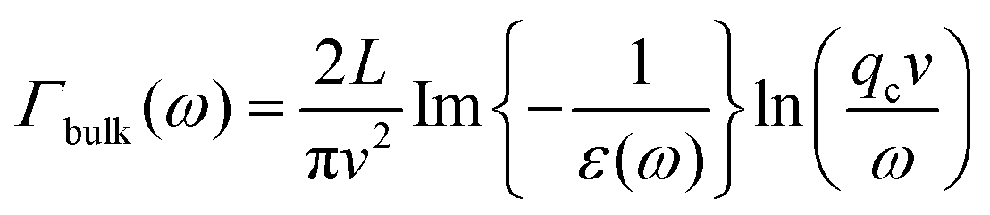
Within the classical dielectric theory, in the local approximation, the target is described as a continuous medium with a frequency-dependent dielectric response function ε(ω). In this description, the total energy loss probability, for general trajectories penetrating the particle, is obtained as the sum of two contributions:| ΓEELS(ω) = Γboundary(ω) + Γbulk(ω), | (17) |
 | (18) |
The first term Γboundary(ω) in eqn (17) is due to the collective excitations of the electron gas at the surface, LSPs, and its dependence on the electron impact parameter is calculated by solving Maxwell's equations with the appropriate boundary conditions at the interfaces separating different media. For spherical particles, this contribution is given by analytical expressions widely used in the literature, which describe the superposition of multipolar plasmon modes.30,82 Nevertheless, in order to describe more precisely the shape of real NPs, numerical methods must be considered to calculate the induced electric field and evaluate eqn (2). In this work we use the BEM (boundary element method), as implemented in the MNPBEM Matlab toolbox,32 which only requires the discretization of the boundary surfaces, instead of the whole volume of the different dielectric media.
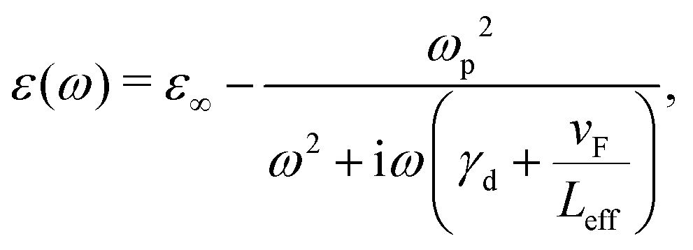
For the small size of the NP considered in the present study, which is below the intrinsic mean free path of conduction electrons in bulk metals, surface scattering has to be considered. We assume this effect, which leads to a reduced effective mean free path Leff, by including a correction to the damping factor in the free electron model (Drude model) of the bulk metal, following the prescriptions in the literature.83 When the specular reflection of electrons at the boundaries is assumed, as in the so-called Billiard model,84 the effective mean free path is given by Leff = 4V/A, where V and A are the volume and area of the particle, respectively.85 Therefore, we adopt the Drude model of the dielectric function given by:
 | (19) |
3 Results and discussion
We explore theoretically within TDDFT the sensitivity of valence-EELS to the specific atomistic structure of a NP, by addressing the energy loss spectrum of a sodium nanocluster composed of 380 atoms probed by 100 keV electrons.First, we select three representative trajectories, all of them crossing the center of the NP, but penetrating it through (i) a vertex, (ii) an edge, and (iii) a facet, as represented in Fig. 2(a); afterwards we vary the electron impact parameter.
 | ||
| Fig. 2 (a) Three electron beam trajectories with kinetic energy Ek = 100 keV crossing the center of a Na380 nanocluster, but penetrating it through different icosahedron symmetry axes, with the entry points marked by white crosses (top view) and straight lines (side view): 5-fold, through two opposing vertices (red); 2-fold, through two opposing edges (green); and 3-fold, through two opposing facets (blue). (b) EEL spectra for the three electron trajectories through a Na380 nanocluster as calculated within TDDFT. (c)–(h) Isosurfaces of the imaginary part of the induced charge density for the main excitations observed for each electron trajectory in the EEL spectra. | ||
In order to conduct the interpretation of the results, and to separate effects derived from electron quantum behavior and those related to the atomistic shape of the cluster, we perform additional calculations within a classical local dielectric framework and using the MNPBEM.32 In these calculations, we consider similar configurations of a NP with abrupt interfaces: (i) a regular icosahedron resembling the atomistic structure of the nanocluster (with smoothened edges and vertices as in ref. 62); (ii) a smoothened icosahedral NP mimicking the shape of the electronic cloud in the atom cluster, which would capture rounding effects derived from the atomistic geometry [see Fig. S1 in the ESI† and insets in Fig. 3(a and b)]; and (iii) a perfectly spherical NP (radius a = 1.85 nm), as a benchmark of the NP shape commonly used in the literature.
 | ||
| Fig. 3 (a) EEL spectra for a Na nanoparticle with smooth icosahedral shape and (b) regular icosahedral shape calculated within BEM for three different trajectories crossing each NP through two opposing vertices (red), through two opposing edges (green), and through two opposing facets (blue). The EEL spectrum for a spherical NP is plotted in black in each figure, and the shape of each NP is plotted in the inset. The kinetic energy of the electron beam is Ek = 100 keV for all trajectories. Plots of the imaginary part of the induced charge density plots representing the LSP modes, highlighted with squares in Fig. 2(a) and with diamonds in Fig. 2(b), as calculated with BEM for (c) a spherical Na NP of radius a = 1.85 nm, (d) for a smooth icosahedral NP and (e) for a regular icosahedral NP. | ||
Although the kinetic energy of the electron beam (100 keV) used in our calculations corresponds to v/c ∼ 0.55, where c is the speed of light, we have checked that relativistic effects are negligible for the size of the NP (ωpa/c ∼ 0.05) and impact parameters involved in this work (see Fig. S2 in the ESI†). Indeed, a thorough study on relativistic effects on EELS in spherical NPs demonstrated in ref. 87 that for small NPs (ωpa/c < 0.2) relativistic effects have no influence on the spectra in a range of velocities v/c = 0.3–0.9.
3.1 Atomistic ab initio EEL spectra
First, we analyze the EEL spectra of the Na380 nanocluster calculated within TDDFT, as described in the previous section, for three electron trajectories crossing the center of the NP [Fig. 2(b)], but from different penetrating points: through a vertex, an edge and a facet, as depicted in Fig. 2(a). Notice that for an equivalent NP with perfect icosahedral symmetry, these trajectories would correspond to three different symmetry axes of the icosahedron (5-fold, 2-fold, and 3-fold, respectively). For simplicity, from here on we will refer to these trajectories as “vertex”, “edge” and “facet”.Depending on the trajectory, different peaks emerge in the EEL spectra [Fig. 2(b)], due to the excitation of localized surface plasmons (LSPs): a peak at energy ω = 3.4 eV dominates for the vertex trajectory (red line); the trajectory through the edge (green line) shows two peaks at ω = 3.45 eV and ω = 4.1 eV, the latter more intense; and a peak at ω = 4.05 eV and a shoulder at lower energy are observed for the facet trajectory (blue line). Moreover, a main excitation at ω = 6.35 eV and some shoulders at lower and higher energies are observed for all three trajectories (with some slight differences in intensity), which we attribute to the excitation of confined bulk plasmons (CBPs), as we will describe later on.
To get further insight into the footprints of atomic-scale features in these EEL spectra, we explore in Fig. 2(c–h) the nature of the identified plasmon excitations by plotting the imaginary part of the associated induced charge density distributions at the nanocluster surface (isosurfaces). The isosurface corresponding to the lowest energy LSP at ω = 3.4 eV, excited for the vertex electron trajectory, shows a quadrupolar pattern [Fig. 2(c)], in which the phase of the induced charge density is the same at the entry and exit points of the electron trajectory, similar to what is observed in small spherical NPs [to be observed later in Fig. 3(c)]. Nevertheless, compared to the quadrupolar plasmon (QP) excited in spherical NPs, the charge density distributions for the nanoclusters in Fig. 2(c) preserve the crystallographic shape of the underlying atomistic structure. Notice the strong charge localization around the vertices and a characteristic five-pointed star-like charge distribution around the electron path, directly related to the 5-fold symmetry of the NP with probed by the vertex electron trajectory. Such strong localization of the charge at the vertices is better visualized in Fig. S3 of the ESI,† where we show the induced charge density plotted at a continuous surface surrounding the atom cluster, i.e., at the surface defining the smooth icosahedron used in the BEM calculations (see Methods).
The induced charge density distributions in Fig. 2(d) corresponding to the LSP excited for the edge trajectory (ω = 4.1 eV, green) show a 2-fold symmetry pattern imposed by this trajectory orientation, with strong charge localization at the vertices and rhomboid-like patterns in the surface around the electron path.
For the facet trajectory (ω = 4.05 eV, blue) the charge density distribution in Fig. 2(e) is ruled by the 3-fold symmetry of the electron trajectory, showing a triangular-like pattern. Notice the difference with the distribution observed for the edge trajectory [Fig. 2(d)], although the peaks observed in the EEL spectra [Fig. 2(b)] are close in energy, meaning that different LSP modes (or sets of LSP modes) are excited for each trajectory. Nevertheless, for both trajectories, there is a charge accumulation at the vertices, characteristic of corner-like plasmonic excitations (also referred to as vertex-like in the literature).88
In contrast, the surface charge density distributions of the CBPs excited at ω = 6.35 eV for all the three trajectories [Fig. 2(f–h)] do not show such strong dependence on the orientation of the electron trajectory with respect to the NP. In fact, due to the nature of the CBPs, i.e., electron collective oscillations localized in the volume of the NP, these oscillations mainly depend on the size of the nanoparticle, rather than on the atomistic morphology of the surface.
3.2 Local classical description of atomic-scale features
As illustrated in Fig. 2(b), the crystallographic structure of the nanoclusters breaks the spherical symmetry commonly assumed for NPs in EELS analysis, resulting in different spectra for different beam penetration points, thus lifting the plasmon energy degeneracy with respect to the multipolar modes of a spherical NP and giving rise to plasmon energy shifts89 and splittings.88We compare the results of the atomistic study with those from classical dielectric theory calculations within the BEM, considering NPs of continuous abrupt boundaries mimicking the crystallographic surface structure of the Na380 nanocluster considered above. The dependence of the calculated EEL spectra on the NP's geometry and orientation of the beam trajectory is explored in Fig. 3, where results obtained within a local dielectric approach for two model NPs, of regular icosahedron and smooth icosahedron shapes, are presented for direct comparison with the TDDFT spectra of the nanocluster. This comparison aims to reveal the accuracy and the intrinsic limitations of classical local dielectric theories commonly used in the literature. In Fig. 3(a and b) the spectra for the two selected model NPs (see insets) are displayed together with the energy loss spectrum for a spherical NP of similar size (a = 1.85 nm), given as a benchmark. More details of the numerical BEM and the dielectric approach used are contained in the Methods section and Section S1 of the ESI.†
The spectra for the irregular smoothened icosahedron NP are plotted in Fig. 3(a) for the same trajectories (vertex, edge, and facet) considered in the TDDFT calculations. Notice that the LSP peaks are shifted with respect to the QP peak at ω = 3.8 eV of the spherical NP used for reference (black line): to the red (ω = 3.6 eV, red line) for the vertex electron trajectory, and to the blue for the edge (ω = 4.0 eV, green line) and facet (ω = 4.1 eV, blue line) trajectories. Moreover, there is a peak at ω = 5.9 eV in all the spectra, at the energy of bulk plasmon (BP) in Na. Direct comparison with Fig. 2(b) demonstrates that these spectra closely match those obtained within TDDFT, reproducing correctly the same plasmon shifts with respect to the QP mode of the spherical NP. In contrast, the spectra for the regular icosahedron NP displayed in Fig. 3(b) show three clearly distinguished LSP peaks for the three electron trajectories; at ω = 3.3 eV for the vertex trajectory (red line), at ω = 3.9 eV for the edge trajectory (green line), and at ω = 4.2 eV for the facet trajectory (blue line).
For such small NPs, the exclusive excitation of even modes can be explained by symmetry arguments.82 In the case of a spherical NP excited by a central beam, only m = 0 modes are excited due to the azimuthal symmetry of the excitation. The external potential produced by the electron beam shows the dependence Vext(r,ω) ∼ eiωz/v, in the non-retarded approximation, so that the phase variation inside a spherical NP of radius a for such trajectory is given by 2ωa/v. In the present study (a < 2 nm, Ek = 100 keV, ωp ∼ 6 eV), the phase variation is almost negligible (2ωpa/v ∼ 0.2 ≪ π), thus the external potential is almost constant along the electron path inside the NP, and mainly even multipolar l modes are excited in the particle, as the phase of the induced charge density at the entry and exit points of the electron remains unchanged.28 Nevertheless, notice that changing the size of the NP or the kinetic energy of the electron beam will alter the relative intensity of the modes in the spectra [see Fig. S2 of the ESI† for results with electron beams of different kinetic energies].
The differences observed between the spectra of the two model NPs and the spherical one in Fig. 3(a and b) are a direct consequence of their different underlying symmetry and corresponding LSP mode structure, which is more clearly reflected in the induced charge density distributions plotted in Fig. 3(c–e). It is observed that the induced charge density profiles clearly follow the NP symmetry around the electron path, corresponding to the three strategic penetration points considered. The side views for the same charge density distributions of Fig. 3(c–e) are also represented in Fig. S3 (ESI†), showing the nature of the LSPs at a glance. As a consequence of well-defined geometrical features, the regular icosahedron shows characteristic charge accumulation at the edges for the edge and facet electron trajectories, as compared to the smooth icosahedron [Fig. 3(d)] and the atom nanocluster [Fig. 2(c–e)], which increase the energy splitting between the modes.88,89 Such splitting is illustrated in Fig. 4, where the energies of the main peaks from the EEL spectra of Fig. 2(b) and 3(a and b) for the central trajectories are compared, evidencing the influence of the shape on the modal structure. For a more quantitative comparison of the mode energies see Section S3 in the ESI.†
 | ||
| Fig. 4 Comparative energy diagram of the main plasmonic excitations observed in the EEL spectra obtained for the four Na NP shapes and central trajectories considered in Fig. 2(b) and 3(a and b). | ||
The most intense peak in the EEL spectra for penetrating electron trajectories appears at ω = ωp = 5.9 eV, which corresponds to the BP in Na. Contrary to the behavior observed in the ab initio calculated spectra for the nanocluster [Fig. 2(b)], in the spectra calculated within the classical dielectric framework [Fig. 3(a and b)] the energy of the bulk plasmon is independent of the NP's shape (sphere, smooth icosahedron or regular icosahedron) and electron trajectory orientation [see Fig. 4], as the contribution of the bulk plasmons to the energy loss probability is introduced ad hoc (see eqn (18) and (19) in the Methods section). More interestingly, the induced charge density distributions of the BP, on the right column of Fig. 3(c–e) show a strong charge localization around the electron path for the BP, but no charge oscillations (phase change) at the surface, in contrast to the TDDFT results [Fig. 2(f–h)].
3.3 Impact parameter dependence
So far we have focused on a particular set of electron trajectories crossing the center of the atom cluster or NPs (impact parameter b = 0), but in STEM the electron beam scans the NPs, producing EEL spectra and plasmon maps for a wide range of impact parameters and trajectories, passing by or through the NP. We study here general penetrating and grazing trajectories [Fig. 5(a)], in order to explore the influence of the atomistic features of the nanocluster on the excitation of different modes as a function of electron beam impact parameter. To complete this study, and in the spirit of the previous section, we test to what extent local classical approaches that properly describe the shape of the NP (smooth icosahedron, [Fig. 5(b)]) can match the impact-parameter dependent EEL spectra provided by the ab initio atomistic TDDFT calculations. We also take the spherical NP [Fig. 5(c)] of similar size as a reference. | ||
| Fig. 5 (a) Atomistic cluster and set of electron trajectories labeled as “near-facet” for a specific orientation of the NP for which the electron trajectories pass near the facet (the atoms forming the facet are highlighted in cyan). (b) Color map of EEL spectra as a function of electron impact parameter b for “near-facet” electron trajectories calculated within ab initio atomistic TDDFT. The peaks corresponding to different plasmon modes are highlighted by bullet points and labeled as surface (S) or bulk (B) modes. (c) EEL spectra from (b), for impact parameters b = 0 nm (blue line), b = 0.5 nm (red line), b = 1 nm (green line), b = 1.5 nm (magenta line), and b = 3 nm (amber line). (d) Smooth icosahedron used in BEM calculations with the same orientation and corresponding “near-facet” electron trajectory set. (e) Color map of EEL spectra as a function of electron impact parameter b for “near-facet” electron trajectories calculated within BEM for the smooth icosahedron, and (f) EEL spectra corresponding to selected trajectories as in (c). (g) Spherical NP used in BEM calculations and electron trajectories, with its corresponding impact parameter dependent EEL spectral colormap, (h) with LSPs labeled according to their l-number and (i) EEL spectra for specific impact parameters as in (c) and (f). The kinetic energy of the electron beam is Ek = 100 keV in all cases. | ||
The main results are presented in Fig. 5(b), where the colormap shows the dependence of the EEL spectra on impact parameter, as calculated within the ab initio atomistic TDDFT, for electron trajectories parallel to the nearest facet of the nanocluster (the atoms forming the facet are highlighted in cyan) in Fig. 5(a). We label these trajectories as “near-facet”. In addition, five representative spectra corresponding to impact parameters b = 0, 0.5, 1, 1.5 and 3 nm of trajectories sketched in Fig. 5(a) are highlighted in Fig. 5(c).
For external trajectories  the spectra are dominated by the excitation of LSPs; there is no trace of CBPs (they are distinguishable only if a logarithmic scale is used, as shown in Fig. S4, ESI†). In particular, for trajectories far from the NP, such as b = 3 nm, the main excitation is the dipolar plasmon (DP) (labeled as S1) at ω = 3.2 eV, as happens in optical spectra.61,62 As the electron trajectory approaches the NP surface, the intensity of the energy loss increases, especially the relative intensity of high-order plasmon (HOP) modes (labeled as S3), which are more sensitive to the rapidly decaying field created by the electron beam, in contrast to the DP. Notice that the energy of the S3 peak (ω = 4.1 eV) closely matches the energy of the mode excited for the edge axial trajectory plotted in Fig. 2(b).
For penetrating trajectories (b < 1.5 nm), together with the LSPs, around the Na bulk plasmon energy a broad excitation consisting of a bunch of CBPs emerges. Notice that the intensity of this broad excitation is highly sensitive to the impact parameter of the electron beam and does not emerge immediately just when the electron trajectory starts to penetrate the cluster, but it requires a minimum L distance inside the NP to be efficiently excited. Regarding the LSPs, the DP mode (S1) dominates the spectrum only for trajectories close to the surface  , with a the NP's radius. As the impact parameter decreases, the QP mode (S2) at ω = 3.4 eV gains strength, consistent with the results for axial trajectories, plotted in Fig. 2(b). This transition from the S1 to the S2 mode for small impact parameters clearly illustrates the deactivation of the DP as b → 0, which is forbidden by symmetry. In turn, when the electron trajectory approaches the NP axis, HOP modes (S3) are efficiently excited.
As mentioned above, similar to the LSPs in Fig. 5(b), the energy losses corresponding to CBPs also show impact parameter dependence: for b = 1 nm a single peak (B2) at ω = 5.9 eV is observed, for b = 0.5 nm there is an additional CBP (B4) at ω = 6.5 eV, and for the central trajectory b = 0 nm, two different excitations are induced at ω = 5.6 eV (B1) and ω = 6.35 eV (B3). These modes are the signature of boundary confinement effects on the longitudinal collective electron oscillations induced inside the NP by the electron beam. The excitation of CPB modes in spherical NPs by light, or by external electron beam trajectories, has been described using hydrodynamic models,49,50 but their contribution is rather small. In contrast, for penetrating electron beam trajectories, CBPs can be efficiently excited and directly observed in the spectra. Although CBP modes have received less attention than LSPs in the literature, shifts of bulk plasmon energies detected in EELS experiments37,43,90 could be explained by the existence of different CBPs, whose excitation depends on the relative impact parameter, as it occurs with LSPs. Additional calculations of EEL spectra for the other two trajectory sets (“near-edge” and “near-vertex”) are presented in Fig. S5 (ESI†), and demonstrate that CBPs are rather insensitive to the NP orientation, contrary to the LSPs.
To get further insight into the characteristics of the EEL spectra of the nanocluster calculated with TDDFT, and to identify their geometrical or quantum origin, we compare them with additional classical calculations for icosahedral and spherical NPs, as we did for the axial trajectories. Fig. 5(e and f) contain the EEL spectra for the “near-facet” electron trajectory set in the smooth icosahedral NP (“near-edge” and “near-vertex” electron trajectory sets are presented in Fig. S6, ESI†). Both classical and TDDFT spectra show similar general trends for the LSPs: (i) excitation of the DP (S1) at ω = 3.35 eV for external trajectories with large impact parameters (b ≫ a), (ii) excitation of HOP modes (S3) at ω = 4.0 eV for grazing trajectories b∼a and penetrating trajectories b < a, and (iii) excitation of the QP mode (S2) at ω = 3.6 eV for small impact parameters. Moreover, a direct comparison between individual trajectory sets for both models shows that the classical calculations qualitatively capture the spectral features observed in the TDDFT calculations. Nevertheless, there is an increased relative intensity of the S3 modes in the local classical spectra as compared to the atomistic ones, which may be attributed to non-local effects included in TDDFT but not accounted for in the classical dielectric description.91 Furthermore, the small discrepancies observed in the LSP energies can be attributed to quantum effects not considered within the BEM calculations. For reference, we have considered a spherical NP of radius a = 1.5 nm [Fig. 5(g)] enclosing the nanocluster Na380 and calculated its EEL spectra as a reference [Fig. 5(h and i)]. In contrast to the smooth icosahedron NP, it is worth noting that the spherical NP model fails to reproduce even qualitatively the LSP spectra of the nanocluster for penetrating and grazing trajectories, in particular the gap between modes S2 and S3.
Importantly, the local classical dielectric approach fails to reproduce the spectral features observed in the TDDFT calculated spectra around the Na bulk plasma energy. In particular, a sharp bulk plasmon is excited for penetrating trajectories at the same energy ω = 5.9 eV, independently of impact parameter or NP shape, as for the axial trajectories b = 0 displayed in Fig. 3(a). One may conclude that the trends of the CBPs obtained with the TDDFT are due to the quantum confinement effects of the electron collective oscillations in the volume of the NP. As explained above, these confinement effects may be described within hydrodynamical models of spherical NPs, which describe the interferences in the electron oscillations in the volume of the NP, bouncing at the spherical boundary.49,92
3.4 Charge density distributions of LSPs and CBPs
In this section, we analyze the features of the induced charge densities [Fig. 6] corresponding to the characteristic plasmonic excitations discussed above [Fig. 5], with special emphasis on the LSPs. We briefly comment on the charge density plots of the CBPs, and point out hints to understand their involved quantization scheme. | ||
| Fig. 6 (a) Isosurfaces of the imaginary part of the charge density for the different modes highlighted in Fig. 5(b) for impact parameters b = 0, 0.5, 1, 1.5, 3 nm. Imaginary part of the induced surface charge density corresponding to the different modes highlighted in Fig. 5(e and h) for (b) a smooth icosahedron and (c) a sphere, respectively, calculated using BEM. | ||
Following the same strategy of Section 3.2, we compare the charge distributions of the nanocluster with those of the classical smooth icosahedral NP mimicking the cluster geometry [Fig. 6(b)] and the reference spherical NP [Fig. 6(c)]. As observed in Fig. 6(b), the smooth icosahedral NP captures the impact parameter-dependent evolution of the charge distributions of the DP (S1), QP (S2), and HOP modes (S3) excited for the “near-facet” electron trajectory, reproducing the atomic-scale features and detailed patterns of the induced charge densities calculated within ab initio atomistic TDDFT [Fig. 6(a)]. See also Fig. S7 and S8, ESI† for the “near-edge” and “near-vertex” trajectories. However, the induced charge densities of the spherical NP plotted in Fig. 6(c), corresponding to the DP (l = 1), QP (l = 2), and HOP (l = 3), obviously miss the atomic-scale features.
As opposed to LSPs, which are localized at the surface, the charge oscillations of the CBPs occur inside the volume of the NP, and therefore their excitation does not show great dependence on the orientation of the NP [see Fig. S5, ESI†]. Thus, in principle CBPs can be properly addressed within hydrodynamic models (HDM) that consider spherical NPs,47,49,92 within which the CBP modes are characterized by (l,n) angular and radial integer numbers. Notice that CBPs follow similar symmetry rules as the LSPs so that odd l-number modes are not excited in small NPs probed by swift electron beams with axial trajectory. From a deeper analysis of the dispersion relation for plasmons in spherical NPs within the HDM, along with the symmetry rules, one can infer that the CBPs that best match the TDDFT results are: B1 as (l,n) = (0,1), B2 as (1,1), B3 as (2,1) and B4 as (3,1). It is worth noting that a description of how these volume plasmons are excited for different impact parameters of the electron probe requires the complete expression of the EEL probability in the HDM, including both external and penetrating trajectories. For the latter, our TDDFT calculations demonstrate that the CBPs are much more efficiently excited, but the analytical EEL expression obtained within HDM is more complicated and deserves further attention, which is out of the scope of the present study.92
It is worth mentioning that the relaxation of the structure produces slightly different lengths in different directions, reducing the symmetry of the system, and thus inducing slight plasmonic mode splitting, as we show in Section 3.1. In this regard, a different choice of the xc-functional within DFT, may affect the EEL spectra. For instance, it is well known that within DFT, LDA underestimates the lattice parameter of Na, and therefore overestimates the electron density and plasma energy, while GGA, provides a more accurate value of the lattice parameter and plasma energy.61,62 On the other hand, concerning the xc-kernel used in TDDFT, it has been shown that TDDFT-LDA and TDDFT-GGA give similar results for the optical response of Ag nanoclusters (relaxed using DFT-GGA),57 thus one would expect just minor corrections from the use of the GGA-PBE kernel.
In summary, atomistic TDDFT offers a framework that naturally integrates all the above-mentioned effects and can therefore serve as a benchmark. Such considerations can help to understand, and hopefully straighten, some disagreements observed between experiments and theory in the literature, especially regarding models in which the specific shape of the NPs has not been properly considered.
4 Conclusions
We have studied theoretically the valence-EEL spectra of a nanocluster composed of 380 Na atoms using an efficient ab initio TDDFT formalism. This size is especially interesting because it lies at the border between the systems studied in cluster physics and those tackled in nanoparticle plasmonics. We have shown that the atomistic features of a NP greatly influence its plasmonic response and thus, they need to be properly accounted for in a full description of EELS experiments at this NP size level. In addition to the particular atomistic morphology of the nanoparticle, TDDFT includes naturally all the quantum effects associated with the electron response.Much of the discussion from previously published papers about EELS in NPs is focused on quantum size effects, namely the shift of the dipolar surface plasmon, to the red or to the blue (depending on the material), when their radius is decreased below 2 nm. Different phenomenological descriptions have been implemented in the literature to explain these shifts, including quantum effects as electron spill-out,44–46,48 dispersion in the dielectric response49,50 or dielectric functions which account for quantum confinement.43 In general, these studies assume spherical NP shapes and do not consider the atomic-scale structure which, as we have shown, clearly affects the EEL spectra for grazing and penetrating trajectories, in particular regarding the mode structure and charge localization at the vertices. So, the specific atomic surface structure should be considered when interpreting the results in EELS experiments, as small NPs usually show polyhedral shapes that exhibit well-defined faces, edges and vertices, with the icosahedron being a frequent motif.35,36
The NP shape effect on the LSPs and CBPs in calculated EELS spectra has been explored by taking as a reference the TDDFT spectra, and comparing them with those calculated within a classical local dielectric approach for two levels of description of the NP geometry: (i) the polyhedral shape with sharp features based on the atomistic structure of the cluster, and (ii) the approximated shape of the NP's surface obtained from DFT calculations, which shows a smoother shape than the former one. This comparison concludes that the latter provides better agreement regarding the mode structure, concerning both the spectral peak distribution and corresponding induced charge density distributions.
The influence of the electron beam orientation and impact parameter observed in the atomistic TDDFT-EEL spectra are also well reproduced by the classical local approach, except for slight differences arising mainly due to electron spill-out and non-local effects. These results are also compared with those obtained for a spherical NP, as a benchmark, showing shifts of a few hundreds of meV, and highlighting the importance of considering the full atomic-scale configuration of the NP, with special mention to the characteristic charge localization at the vertices of atomistic NPs.
On the other hand, the excitation of longitudinal electron oscillations inside the volume of the NPs, the so-called CBPs, are inherently included in the TDDFT framework. We have shown that their relative contribution to the spectrum for penetrating trajectories is as important as that of LSPs. In this spectral region, contrary to the LSPs, local dielectric models with boundaries resembling the atomistic shape of the nanocluster are not able to account for the rich footprints of the CBP spectral region, neither for the intensity nor for the width of the CBPs or their sensitivity to the impact parameter.
We have shown that ab initio atomistic TDDFT offers a state-of-the-art framework to study the interaction of electron beams with small NPs showing atomistic geometrical features. Although we have focused on a Na nanocluster, TDDFT can be applied to a wide variety of materials, including Ag NPs, which are still the object of much discussion in the literature.63 In principle, the detection of atomic-scale features and diverse CBPs in the EEL spectra is at hand with the spatial and energy resolution obtained nowadays in STEM microscopes. Thus, although challenging to detect experimentally, our results can motivate further research on EELS by revealing atomic-scale features. Moreover, these features would further enhance the interaction between plasmons and matter attached to the one atom-size vertices of NPs, opening the possibility to perform extreme field-enhanced EELS.
Conflicts of interest
There are no conflicts to declare.Acknowledgements
Financial support from Project No. PID2022-139579NB-I00 of MICIN, project of the Basque Department of Education (Grant No. IT1526-22) are acknowledged. M. U. acknowledges support from DIPC and CFM. D. S. P. acknowledges support from Grants PID2019-107338RB-C66 and PID2022-140845OB-C66 funded by MCIN/AEI/10.13039/501100011033, and the Basque Department of Education (Grant IT1569-22). M. B. acknowledges support from the Departamento de Educación of the Basque Government through a PhD grant, as well as from Euskampus and the DIPC at the initial stages of this work. P. K. acknowledges financial support from the Fellows Gipuzkoa program of the Gipuzkoako Foru Aldundia through the FEDER funding scheme of the European Union, “Una manera de hacer Europa”.Notes and references
- C. J. Powell and J. B. Swan, Phys. Rev., 1959, 116, 81–83 CrossRef CAS.
- N. D. Browning, M. F. Chisholm and S. J. Pennycook, Nature, 1993, 366, 143–146 CrossRef CAS.
- P. E. Batson, Nature, 1993, 366, 727–728 CrossRef CAS.
- R. Egerton, Electron Energy-Loss Spectroscopy in the Electron Microscope, Springer, US, Boston, MA, 2011 Search PubMed.
- O. L. Krivanek, T. C. Lovejoy, N. Dellby, T. Aoki, R. W. Carpenter, P. Rez, E. Soignard, J. Zhu, P. E. Batson, M. J. Lagos, R. F. Egerton and P. A. Crozier, Nature, 2014, 514, 209–212 CrossRef CAS PubMed.
- P. E. Batson, N. Dellby and O. L. Krivanek, Nature, 2002, 418, 617–620 CrossRef CAS PubMed.
- O. L. Krivanek, M. F. Chisholm, V. Nicolosi, T. J. Pennycook, G. J. Corbin, N. Dellby, M. F. Murfitt, C. S. Own, Z. S. Szilagyi, M. P. Oxley, S. T. Pantelides and S. J. Pennycook, Nature, 2010, 464, 571–574 CrossRef CAS PubMed.
- N. Grillet, D. Manchon, F. Bertorelle, C. Bonnet, M. Broyer, E. Cottancin, J. Lermé, M. Hillenkamp and M. Pellarin, ACS Nano, 2011, 5, 9450–9462 CrossRef CAS PubMed.
- D. O. Sigle, J. Mertens, L. O. Herrmann, R. W. Bowman, S. Ithurria, B. Dubertret, Y. Shi, H. Y. Yang, C. Tserkezis, J. Aizpurua and J. J. Baumberg, ACS Nano, 2015, 9, 825–830 CrossRef CAS PubMed.
- P. Hawkes, Ultramicroscopy, 2015, 156, A1–A64 CrossRef CAS PubMed.
- Q. M. Ramasse, Ultramicroscopy, 2017, 180, 41–51 CrossRef CAS PubMed.
- S. J. Pennycook, in Scanning Transmission Electron Microscopy, ed. S. J. Pennycook and P. D. Nellist, Springer New York, New York, NY, 2011, pp. 1–90 Search PubMed.
- X. Ke, C. Bittencourt and G. Van Tendeloo, Beilstein J. Nanotechnol., 2015, 6, 1541–1557 CrossRef CAS PubMed.
- P. D. Nellist, Science, 2004, 305, 1741 CrossRef CAS PubMed.
- J. L. Hart, A. C. Lang, A. C. Leff, P. Longo, C. Trevor, R. D. Twesten and M. L. Taheri, Sci. Rep., 2017, 7, 8243 CrossRef PubMed.
- M. J. Lagos, A. Trügler, U. Hohenester and P. E. Batson, Nature, 2017, 543, 529–532 CrossRef CAS PubMed.
- A. A. Govyadinov, A. Konecná, A. Chuvilin, S. Vélez, I. Dolado, A. Y. Nikitin, S. Lopatin, F. Casanova, L. E. Hueso, J. Aizpurua and R. Hillenbrand, Nat. Commun., 2017, 8, 95 CrossRef PubMed.
- P. M. Zeiger and J. Rusz, Phys. Rev. Lett., 2020, 124, 25501 CrossRef CAS PubMed.
- H. Lourenço-Martins and M. Kociak, Phys. Rev. X, 2017, 7, 1–11 Search PubMed.
- P. Rez, T. Aoki, K. March, D. Gur, O. L. Krivanek, N. Dellby, T. C. Lovejoy, S. G. Wolf and H. Cohen, Nat. Commun., 2016, 7, 10945 CrossRef CAS PubMed.
- J. A. Hachtel, J. Huang, I. Popovs, S. Jansone-Popova, J. K. Keum, J. Jakowski, T. C. Lovejoy, N. Dellby, O. L. Krivanek and J. C. Idrobo, Science, 2019, 363, 525–528 CrossRef CAS PubMed.
- O. Nicoletti, F. De La Peña, R. K. Leary, D. J. Holland, C. Ducati and P. A. Midgley, Nature, 2013, 502, 80–84 CrossRef CAS PubMed.
- A. Hörl, G. Haberfehlner, A. Trügler, F.-P. Schmidt, U. Hohenester and G. Kothleitner, Nat. Commun., 2017, 8, 37 CrossRef PubMed.
- P. E. Batson, Phys. Rev. Lett., 1982, 49, 936–940 CrossRef CAS.
- P. E. Batson, Ultramicroscopy, 1982, 9, 277–282 CrossRef CAS.
- A. Rivacoba, N. Zabala and P. M. Echenique, Phys. Rev. Lett., 1992, 69, 3362–3365 CrossRef PubMed.
- N. Zabala, A. Rivacoba and P. M. Echenique, Phys. Rev. B: Condens. Matter Mater. Phys., 1997, 56, 7623–7635 CrossRef CAS.
- A. Rivacoba, N. Zabala and J. Aizpurua, Prog. Surf. Sci., 2000, 65, 1–64 CrossRef CAS.
- F. J. García de Abajo, Rev. Mod. Phys., 2010, 82, 209–275 CrossRef.
- T. L. Ferrell and P. M. Echenique, Phys. Rev. Lett., 1985, 55, 1526–1529 CrossRef CAS PubMed.
- F. J. García de Abajo and A. Howie, Phys. Rev. B: Condens. Matter Mater. Phys., 2002, 65, 115418 CrossRef.
- U. Hohenester, Comput. Phys. Commun., 2014, 185, 1177–1187 CrossRef CAS.
- Y. Cao, A. Manjavacas, N. Large and P. Nordlander, ACS Photonics, 2015, 2, 369–375 CrossRef CAS.
- S. Raza, N. Stenger, S. Kadkhodazadeh, S. V. Fischer, N. Kostesha, A.-P. Jauho, A. Burrows, M. Wubs and N. A. Mortensen, Nanophotonics, 2013, 2, 131–138 CrossRef CAS.
- S. Raza, S. Kadkhodazadeh, T. Christensen, M. Di Vece, M. Wubs, N. A. Mortensen and N. Stenger, Nat. Commun., 2015, 6, 8788 CrossRef CAS PubMed.
- A. Campos, N. Troc, E. Cottancin, M. Pellarin, H.-C. Weissker, J. Lermé, M. Kociak and M. Hillenkamp, Nat. Phys., 2019, 15, 275–280 Search PubMed.
- J. A. Scholl, A. L. Koh and J. A. Dionne, Nature, 2012, 483, 421–427 CrossRef CAS PubMed.
- T. Lünskens, P. Heister, M. Thämer, C. A. Walenta, A. Kartouzian and U. Heiz, Phys. Chem. Chem. Phys., 2015, 17, 17541–17544 RSC.
- A. L. Koh, A. I. Fernández-Domínguez, D. W. McComb, S. A. Maier and J. K. W. Yang, Nano Lett., 2011, 11, 1323–1330 CrossRef CAS PubMed.
- H. Duan, A. I. Fernández-Domínguez, M. Bosman, S. A. Maier and J. K. W. Yang, Nano Lett., 2012, 12, 1683–1689 CrossRef CAS PubMed.
- S. F. Tan, L. Wu, J. K. Yang, P. Bai, M. Bosman and C. A. Nijhuis, Science, 2014, 343, 1496–1499 CrossRef CAS PubMed.
- S. Kadkhodazadeh, J. B. Wagner, H. Kneipp and K. Kneipp, Appl. Phys. Lett., 2013, 103, 83103 CrossRef.
- Y. W. Wang, J. S. Kim, G. H. Kim and K. S. Kim, Appl. Phys. Lett., 2006, 88, 3–6 Search PubMed.
- N. D. Lang and W. Kohn, Phys. Rev. B: Solid State, 1970, 1, 4555–4568 CrossRef.
- A. Liebsch, Phys. Rev. B: Condens. Matter Mater. Phys., 1993, 48, 11317–11328 CrossRef CAS PubMed.
- T. V. Teperik, P. Nordlander, J. Aizpurua and A. G. Borisov, Phys. Rev. Lett., 2013, 110, 263901 CrossRef CAS PubMed.
- A. Rivacoba, Ultramicroscopy, 2019, 207, 112835 CrossRef CAS PubMed.
- A. Rivacoba, Phys. Rev. B, 2023, 107, 035401 CrossRef CAS.
- T. Christensen, W. Yan, S. Raza, A.-P. Jauho, N. A. Mortensen and M. Wubs, ACS Nano, 2014, 8, 1745–1758 CrossRef CAS PubMed.
- N. A. Mortensen, S. Raza, M. Wubs, T. Søndergaard and S. I. Bozhevolnyi, Nat. Commun., 2014, 5, 3809 CrossRef CAS PubMed.
- R. Esteban, A. G. Borisov, P. Nordlander and J. Aizpurua, Nat. Commun., 2012, 3, 1–9 Search PubMed.
- J. A. Scholl, A. Garcia-Etxarri, G. Aguirregabiria, R. Esteban, T. C. Narayan, A. L. Koh, J. Aizpurua and J. A. Dionne, ACS Nano, 2016, 10, 1346–1354 CrossRef CAS PubMed.
- P. Koval, M. Barbry and D. Sánchez-Portal, Comput. Phys. Commun., 2019, 236, 188–204 CrossRef CAS.
- P. Koval, D. Foerster and O. Coulaud, J. Chem. Theory Comput., 2010, 6, 2654–2668 CrossRef CAS PubMed.
- D. Sánchez-Portal, P. Ordejón, E. Artacho and J. M. Soler, Int. J. Quantum Chem., 1997, 65, 453–461 CrossRef.
- J. M. Soler, E. Artacho, J. D. Gale, A. García, J. Junquera, P. Ordejón and D. Sánchez-Portal, J. Phys.: Condens. Matter, 2002, 14, 2745–2779 CrossRef CAS.
- P. Koval, F. Marchesin, D. Foerster and D. Sánchez-Portal, J. Phys.: Condens. Matter, 2016, 28, 214001 CrossRef PubMed.
- M. Barbry, PhD thesis, University of the Basque Country, UPV-EHU, San Sebastian, 2018.
- P. Zhang, J. Feist, A. Rubio, P. García-González and F. J. García-Vidal, Phys. Rev. B: Condens. Matter Mater. Phys., 2014, 90, 161407 CrossRef.
- M. Kuisma, A. Sakko, T. P. Rossi, A. H. Larsen, J. Enkovaara, L. Lehtovaara and T. T. Rantala, Phys. Rev. B: Condens. Matter Mater. Phys., 2015, 91, 115431 CrossRef.
- M. Barbry, P. Koval, F. Marchesin, R. Esteban, A. G. Borisov, J. Aizpurua and D. Sánchez-Portal, Nano Lett., 2015, 15, 3410–3419 CrossRef CAS PubMed.
- M. Urbieta, M. Barbry, Y. Zhang, P. Koval, D. Sánchez-Portal, N. Zabala and J. Aizpurua, ACS Nano, 2018, 12, 585–595 CrossRef CAS PubMed.
- H. Haberland, Nature, 2013, 494, 6–7 CrossRef PubMed.
- N. Zabala and A. Rivacoba, Phys. Rev. B: Condens. Matter Mater. Phys., 1993, 48, 14534–14542 CrossRef CAS PubMed.
- Z. Wang, Micron, 1996, 27, 265–299 CrossRef CAS.
- R. H. Ritchie and A. Howie, Philos. Mag. A, 1988, 58, 753–767 CrossRef.
- J. N. Murrell and R. E. Mottram, Mol. Phys., 1990, 69, 571–585 CrossRef CAS.
- E. G. Noya, J. P. Doye, D. J. Wales and A. Aguado, Eur. Phys. J. D, 2007, 43, 57–60 CrossRef CAS.
- D. J. Wales, J. P. K. Doye, A. Dullweber, M. Hodges, F. Naumkin, F. Calvo, J. Hernández-Rojas and T. F. Middleton, The initial structure of the Na380 cluster was downloaded from the Cambridge Cluster Database, https://www-wales.ch.cam.ac.uk/CCD.html.
- J. P. Perdew, K. Burke and M. Ernzerhof, Phys. Rev. Lett., 1996, 77, 3865–3868 CrossRef CAS PubMed.
- J. M. Pruneda, D. Sánchez-Portal, A. Arnau, J. I. Juaristi and E. Artacho, Phys. Rev. Lett., 2007, 99, 235501 CrossRef CAS PubMed.
- K. Tsubonoya, C. Hu and K. Watanabe, Phys. Rev. B: Condens. Matter Mater. Phys., 2014, 90, 35416 CrossRef CAS.
- M. Petersilka, U. J. Gossmann and E. K. Gross, Phys. Rev. Lett., 1996, 76, 1212–1215 CrossRef CAS PubMed.
- K. Yabana and G. F. Bertsch, Phys. Rev. A: At., Mol., Opt. Phys., 1999, 60, 3809–3814 CrossRef CAS.
- H. C. Weissker and X. López-Lozano, Phys. Chem. Chem. Phys., 2015, 17, 28379–28386 RSC.
- D. Foerster, arXiv, 2006, preprint, arXiv:physics/0612187 DOI:10.48550/arXiv.physics/0612187.
- A. García, N. Papior, A. Akhtar, E. Artacho, V. Blum, E. Bosoni, P. Brandimarte, M. Brandbyge, J. I. Cerdá, F. Corsetti, R. Cuadrado, V. Dikan, J. Ferrer, J. Gale, P. García-Fernández, V. M. García-Suárez, S. García, G. Huhs, S. Illera, R. Korytár, P. Koval, I. Lebedeva, L. Lin, P. López-Tarifa, S. G. Mayo, S. Mohr, P. Ordejón, A. Postnikov, Y. Pouillon, M. Pruneda, R. Robles, D. Sánchez-Portal, J. M. Soler, R. Ullah, V. W.-Z. Yu and J. Junquera, J. Chem. Phys., 2020, 152, 204108 CrossRef PubMed.
- Q. Sun, X. Zhang, S. Banerjee, P. Bao, M. Barbry, N. S. Blunt, N. A. Bogdanov, G. H. Booth, J. Chen, Z.-H. Cui, J. J. Eriksen, Y. Gao, S. Guo, J. Hermann, M. R. Hermes, K. Koh, P. Koval, S. Lehtola, Z. Li, J. Liu, N. Mardirossian, J. D. McClain, M. Motta, B. Mussard, H. Q. Pham, A. Pulkin, W. Purwanto, P. J. Robinson, E. Ronca, E. R. Sayfutyarova, M. Scheurer, H. F. Schurkus, J. E. T. Smith, C. Sun, S.-N. Sun, S. Upadhyay, L. K. Wagner, X. Wang, A. White, J. D. Whitfield, M. J. Williamson, S. Wouters, J. Yang, J. M. Yu, T. Zhu, T. C. Berkelbach, S. Sharma, A. Y. Sokolov and G. K.-L. Chan, J. Chem. Phys., 2020, 153, 24109 CrossRef CAS PubMed.
- E. Artacho, D. Sánchez-Portal, P. Ordejón, A. García and J. Soler, Phys. Status Solidi B, 1999, 215, 809–817 CrossRef CAS.
- J. D. Jackson, Classical Electrodynamics, Wiley, New York, NY, 3rd edn, 1999 Search PubMed.
- D. Pines and D. Bohm, Phys. Rev., 1952, 85, 338–353 CrossRef CAS.
- A. Rivacoba and P. M. Echenique, Scanning Microsc., 1990, 4, 73–78 Search PubMed.
- A. Moroz, J. Phys. Chem. C, 2008, 112, 10641–10652 CrossRef CAS.
- U. Kreibig and C. v Fragstein, Z. Phys., 1969, 224, 307–323 CrossRef CAS.
- C. Dellago and H. A. Posch, J. Stat. Phys., 1997, 88, 825–842 CrossRef.
- G. W. Luckey, J. Am. Chem. Soc., 1957, 79, 3299 CrossRef.
- F. J. García de Abajo, Phys. Rev. B: Condens. Matter Mater. Phys., 1999, 59, 3095–3107 CrossRef.
- S. A. Mezzasalma, M. Grzelczak and J. Sancho-Parramon, ACS Photonics, 2020, 7, 1551–1559 CrossRef CAS.
- S. M. Collins, Phys. Rev. B, 2018, 97, 245422 CrossRef CAS.
- R. G. Hobbs, V. R. Manfrinato, Y. Yang, S. A. Goodman, L. Zhang, E. A. Stach and K. K. Berggren, Nano Lett., 2016, 16, 4149–4157 CrossRef CAS PubMed.
- S. Raza, S. I. Bozhevolnyi, M. Wubs and N. Asger Mortensen, J. Phys.: Condens. Matter, 2015, 27, 183204 CrossRef PubMed.
- M. Urbieta, PhD thesis, University of the Basque Country, UPV-EHU, 2021.
- F. Benz, M. K. Schmidt, A. Dreismann, R. Chikkaraddy, Y. Zhang, A. Demetriadou, C. Carnegie, H. Ohadi, B. de Nijs, R. Esteban, J. Aizpurua and J. J. Baumberg, Science, 2016, 354, 726–729 CrossRef CAS PubMed.
Footnote |
| † Electronic supplementary information (ESI) available. See DOI: https://doi.org/10.1039/d4cp01034e |
| This journal is © the Owner Societies 2024 |