
Dynamic repulsive interaction enables an asymmetric electron–phonon coupling for improving Raman scattering†
Jiawei
Shen
 a,
Jiaxin
Zhang
a,
Zirui
Fu
a,
Yan
Pan
a,
Xiaowan
Li
a,
Shuyi
Wu
*a,
Yun
Shan
*b and
Lizhe
Liu
*c
a,
Jiaxin
Zhang
a,
Zirui
Fu
a,
Yan
Pan
a,
Xiaowan
Li
a,
Shuyi
Wu
*a,
Yun
Shan
*b and
Lizhe
Liu
*c
aJiangsu Key Laboratory of Micro and Nano Heat Fluid Flow Technology and Energy Application, School of Physical Science and Technology, Suzhou University of Science and Technology, Suzhou, 215009, People's Republic of China. E-mail: wsy@usts.edu.cn
bKey Laboratory of Advanced Functional Materials of Nanjing, Nanjing Xiaozhuang University, Nanjing 211171, People's Republic of China. E-mail: yshan@njxzc.edu.cn
cNational Laboratory of Solid State Microstructures and School of Physics, Nanjing University, Nanjing 210093, People's Republic of China. E-mail: lzliu@nju.edu.cn
First published on 8th February 2024
Abstract
Two-dimensional (2D) materials are an excellent platform for surface-enhanced Raman spectroscopy (SERS). For ReS2, the Raman enhancement effect can be highly improved through the dipole–dipole interactions and synergistic resonance effects in the phase-engineering ReS2 films. However, the performance of the substrate can be improved further through regulating the electronic interaction between the ReS2 and probe molecules. Herein, a dynamic coulomb repulsion strategy is proposed to trigger an electronic state redistribution by asymmetric electrostatic interactions. With the phase-engineering ReS2/graphene heterostructure as a prototype, under laser excitation, the generated hot electrons in graphene and ReS2 can repel each other due to Coulomb interaction, which breaks the symmetrical distribution of hot electrons in ReS2, and increases the electronic concentration at the interface between ReS2 and the probe molecule. With R6G as the probe molecule, the asymmetric electron distribution and synergistic resonance effects on their interface improve the limit of detection to 10−12 M with an EF of 2.15 × 10⁸. Meanwhile, the heterostructure also shows good uniformity, stability as well as unique anisotropy. This strategy can be generalized to other 2D heterostructures to obtain the ultrasensitive SERS substrates.
Introduction
Surface-enhanced Raman spectroscopy (SERS), which depends on the electromagnetic mechanism (EM) and chemical mechanism (CM), is an indispensable candidate method for detecting molecules with extremely high sensitivity, and intensively applied in cross-disciplinary fields including chemistry, biology, agriculture and archaeology.1–5 The EM is attributed to the local electromagnetic fields augmented by local surface plasmon resonance (LSPR) with superior SERS performance, while the CM is mainly induced by the charge transfer associated with complementary effects, say, molecule resonance, exciton resonance, Mie resonance,6etc., between the substrate and the molecule.7–11 Nevertheless, the practical application of EM-based noble metal SERS substrates is hindered by poor surface uniformity, stability and biocompatibility. In contrast, CM-based semiconducting SERS substrates outstrip the scope of EM-based materials and have the potential to overcome these deficiencies.9,12 However, compared with the EM, the CM usually suffers from limited Raman enhancement. Studies have reported that two-dimensional (2D) atomic materials including graphene13–16 and transition metal dichalcogenides (TMDs)17–21 are particularly promising to provide CM enhancement for SERS applications. Especially, for 2D rhenium disulfide (ReS2), our previous work indicates that the excitonic emission can be modulated gradually from the infrared to visible region to achieve μex through the introduction of the T phase.22 Eventually, the Raman enhancement effect can be highly improved through the dipole–dipole interactions and synergistic resonance effects in the phase-engineering ReS2 (T@Td-ReS2) films.23 However, it is still necessary to improve the performance of the substrate further to extend its application.As mentioned above, the CM depends on the charge transfer between the substrate and the molecule. The high electron concentration at the substrate surface can increase the charge transfer probability and thus enhance the SERS performance.12,24 According to Fermi's golden rule,16 the electron transition probability rate (wlk) is formulated as
 | (1) |
 is the matrix element for the LUMO–HOMO transition. Therefore, the increase of the density of state (DOS) will elevate the charge transfer probability, and contribute to the prominent Raman enhancement.24–26 Weng et al. employed Au cluster intercalated bilayer metallic 2H-TaS2 as the SERS substrate, where the DOS on the surface was reinforced by the overlapped d–d orbitals and p–d orbitals between Ta and Au, and S and Au, respectively. The metal-like properties with intrinsic high DOS near the Fermi surface combined with overlapped wave function synergistically contributed to the performance of SERS.25 Lv et al. introduced Nb and/or Re doped WSe2 and it was theoretically and experimentally verified that the Nb/Re co-doped substrate possessed an optimized SERS effect due to the highest DOS facilitating the PICT process. Meanwhile, the adatoms will expand the energy gap of WSe2 to match laser energy, realizing exciton resonance.24 1T′ semimetal W(Mo)Te2 was utilized by Tao et al. to obtain ultrasensitive SERS performance, featuring the increased DOS induced by the unique phase structure of telluride.26 The abovementioned feasible approaches, including doping, substitution and phase engineering, have inspired researchers to develop novel methods to obtain high DOS. However, it is still desirable to develop a simple method to achieve high DOS for excellent SERS performance.
In this work, a new strategy is utilized to obtain large DOS at the interface of the probe molecules and ReS2 by the symmetry breaking of the carrier spatial redistribution. Considering that graphene has prominent electronic properties, high charge mobility and good chemical inertness,27–29 the heterostructure with the graphene on the bottom of phase-engineering ReS2 is assembled. As shown in Fig. 1, the vertically stacked 2D T@Td-ReS2 and graphene (T@Td-ReS2/G) heterojunction is utilized to investigate the SERS effect using rhodamine 6G (R6G) as the probe molecule. When the heterostructure is illuminated by a laser, the generated hot electrons in graphene and ReS2 can repel each other due to Coulomb interaction, which breaks the symmetrical distribution of “hot” electrons in ReS2, results in the increase of the DOS at the interface of R6G and T@Td-ReS2, and hence improves the electron transition efficiency to achieve excellent SERS performance.
 | ||
| Fig. 1 Schematic illustration of the SERS enhancement mechanism in a T@Td-ReS2/G heterostructure system. | ||
Materials and methods
Fabrication of the SERS substrate
The preliminarily synthesized ReS2 with a mixed T phase and Td phase, i.e. T@Td-ReS2, was mechanically exfoliated into thinner layer films.23 Two new peaks located at 122 cm−1 and 129 cm−1 justified the introduction of the T phase in ReS2, as shown in Fig. S1 in the ESI.† Graphene was as well mechanically exfoliated from high oriented pyrolytic graphite (HOPG), which was purchased from Bruker. Graphene was directly attached to a 285 nm SiO2/Si wafer. T@Td-ReS2 was picked up by polydimethylsiloxane (PDMS) and subsequently transferred to graphene using a 2D transferring platform (MetaTest E1) to form a vertically stacked heterostructure. The layer number of graphene can be strictly determined by the shape of the 2D peak, as shown in Fig. S2 in the ESI.†Characterization
The thickness of graphene and T@Td-ReS2 was estimated by the color contrast of the individual optical microscopic image using the objective (Olympus) integrated in a Raman testing device, and further confirmed by atomic force microscopy (AFM, Bruker Multimode 8). The contact mode was used to acquire the AFM image with 0.2 Hz and 512 lines. The effective contact between graphene and T@Td-ReS2 was confirmed by Raman spectra (Horiba LabRAM HR Evolution) of the heterostructure with a 532 nm laser. UV-Vis-NIR absorption spectra (Shimadzu UV3600) were acquired with the wavelength range of 200 nm to 1700 nm. The photoluminescence (PL) spectra were measured on an Edinburgh FLS-920 PL spectrometer, and the time-resolved PL spectra were also acquired on FLS-920 with a monochromatic light from a pulse laser.SERS measurements
Rhodamine 6G (R6G) as well as crystal violet (CV) and methylene blue (MeB) were used as the probe molecules in the experiment. Probe molecule powder was dispersed in deionized water and sequentially diluted to 1 × 10⁻¹⁵ M with the concentration increment of one order of magnitude. The prepared substrate was dripped by probe molecule solution with certain concentration and then placed in a vacuum oven where the temperature was set at 50 centigrade to completely dry it off. The SERS performance was conducted using a confocal Raman testing device (Horiba LabRAM HR Evolution) to collect Raman signals. Raman spectra were acquired using a 532 nm laser with a confocal diameter of ∼700 nm under a × 100 objective lens. The laser energy was set at 1 mW, and the acquisition time and accumulation were 10 s and 1 time, respectively. The mapping mode was also used with the same parameters.Results and discussion
T@Td-ReS2 was successfully transferred on graphene to form the heterostructure, namely, T@Td-ReS2/G whose optical microscope (OM) is shown in Fig. 2a. The thickness of the T@Td-ReS2/G heterostructure was further confirmed by AFM, as shown in Fig. 2b–e, with a typical thickness of 0.4 nm and 3.5 nm for underlying graphene and T@Td-ReS2, respectively. To verify the effective contact between graphene and T@Td-ReS2, the Raman spectra were recorded as given in Fig. 2f, where Raman peaks attributed to ReS2, graphene and the SiO2/Si wafer are distinctly presented. The monolayer graphene was features the single-peak profile of the 2D peak.30 Noticeably, as shown in Fig. 2g, the G peak and 2D peak were upshifted by ∼5 cm−1 and ∼25 cm−1, indicating the interlayer coupling effect between graphene and T@Td-ReS2.31,32 As mentioned above, the “hot” electrons at the interface between graphene and T@Td-ReS2 can repel each other, which leads to the compression of the graphene lattice.32 The lattice compression causes phonon hardening and the frequency increase of the Raman peak. Therefore, the blueshift of the G peak and 2D peak indicates that the interaction between graphene and T@Td-ReS2 exists indeed.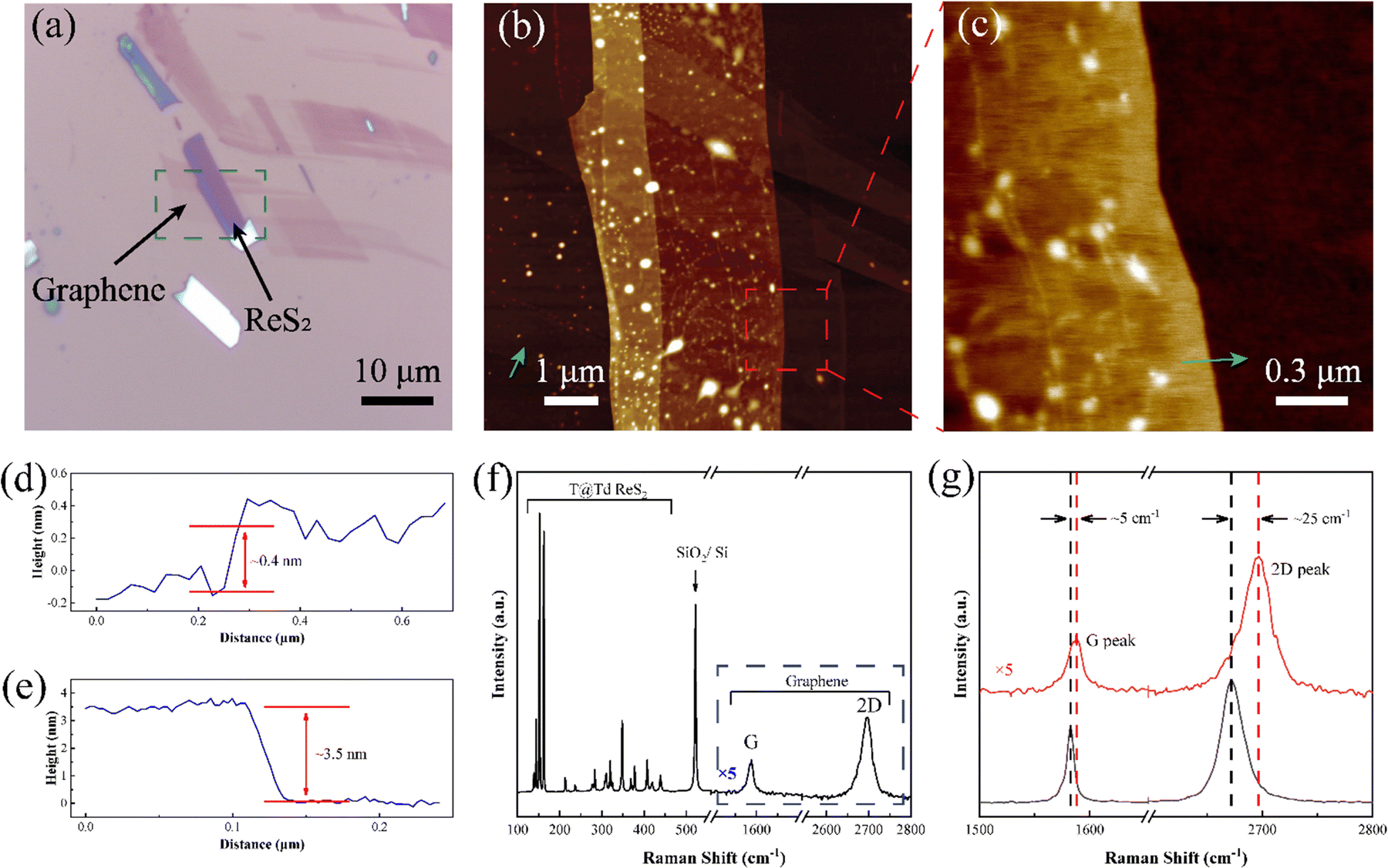 | ||
| Fig. 2 Characterization of a T@Td-ReS2/G heterostructure. (a) Optical microscope of the heterostructure. (b) Atomic force microscope of the heterostructure and (c) selected area indicated in (b). (d) and (e) The height profile of graphene and T@Td ReS2 marked by a green arrow in (b) and (c). (f) Raman spectra of the heterostructure and (g) the upshift of the G peak and 2D peak attributed to graphene (black line: pristine graphene and red line: graphene in the heterostructure). | ||
To investigate the SERS effect of T@Td-ReS2/G, the heterostructure was dripped with rhodamine 6G (R6G) water solution with different concentrations. As shown in Fig. 3a, five Raman peaks located at 611 cm−1 (C–C–C ring in-plane bend), 772 cm−1 (C–H out-of-plane bend), 1361 cm−1, 1510 cm−1 and 1650 cm−1 (aromatic C–C stretching for the last 3 vibrational modes) can be distinctly observed.33,34 The Raman peak at 1580 cm−1 belongs to graphene.30 Besides, no Raman peak of R6G was detected on the SiO2/Si wafer at a concentration of 1 × 10⁻³ M other than the intensive fluorescence background, as shown in Fig. S3 in the ESI.† The LOD was lowered to 1 × 10⁻¹² M according to Fig. 3a compared to 1 × 10⁻⁹ M tested on T@Td-ReS2 in Fig. S4 in the ESI.† Meanwhile, the SERS effect hardly depends on the layer number of ReS2 due to the weak interlayer coupling.35,36 Furthermore, the curve of intensity at 611 cm−1 as a function of probe molecule concentration is plotted in Fig. 3b, indicating a linear response ranging from 1 × 10⁻⁵ M to 1 × 10⁻¹² M, which enables the feasibility of quantitative detection in low concentration.37,38 The enhancement factor (EF) at 611 cm−1 and 772 cm−1 was also calculated and given as 2.15 × 10⁸ and 5.59 × 10⁷, respectively. The detailed EF calculation method has been clarified in the ESI.† The standard Raman spectra of R6G are presented in Fig. S5 in the ESI.† Two more probe molecules, i.e. CV and MeB, were selected to investigate the general enhancement performance of the substrate. The LODs of CV and MeB were 1 × 10⁻¹⁰ M, as shown in Fig. 3c and d, implying the universal application potential.
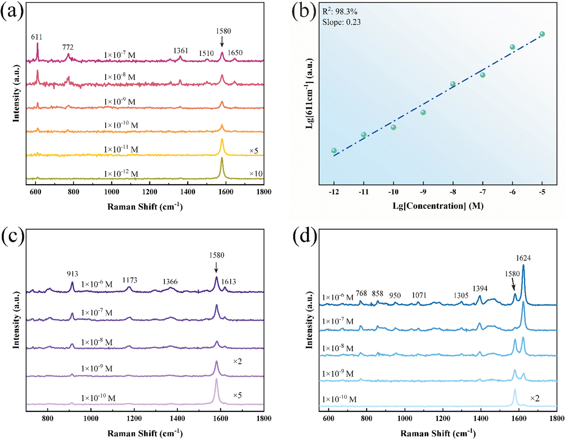 | ||
| Fig. 3 (a) SERS spectra of R6G molecules adsorbed on T@Td-ReS2/G with the concentration varying from 1 × 10⁻⁷ M to 1 × 10⁻¹² M, where the peak located at ∼1580 cm−1 is attributed to graphene. (b) Logarithmic relation of the integrated Raman intensity at 611 cm−1 and R6G concentration, and the corresponding linear fitting curve. (c) and (d) SERS spectra of CV and MeB molecules adsorbed on the heterostructure, respectively, with the LOD both down to 1 × 10⁻¹⁰ M. | ||
Apart from the low LOD and outstanding sensitivity of the substrate system, homogeneity and stability play essential roles in the practical application. Raman mapping was measured to verify the homogeneity of the T@Td-ReS2/G heterojunction. The Raman mapping presented in Fig S6b and c (ESI†) visualized the outstanding spatial uniformity of the substrate. Raman spectra of 50 separate sites inside the marked area in Fig. S6a in the ESI† were acquired at a concentration of 1 × 10⁻⁹ M, as shown in Fig. 4a. Two peaks at 611 cm−1 and 772 cm−1 were selected to calculate the relative standard deviation (RSD) with the values of 6.35% and 11.29%, respectively, as shown in Fig. 4b. Given the low concentration of the probe molecule, the relatively low signal-noise ratio at 772 cm−1 resulted in a high RSD compared to that at 611 cm−1. Meanwhile, our system still retained excellent SERS performance after the exposure to air for 3 months. A robust signal justified the time reproducibility of our substrate, as shown in Fig. 4c. The intensity heat map presented in Fig. S6b and c in the ESI† visualized the spatial uniformity of the substrate. In addition, our previous works indicate that the Raman enhancement of the probe molecules is anisotropic due to the angular dependence of the charge distributions on T@Td-ReS2.23 Herein, angle-resolved polarized Raman spectra of T@Td-ReS2 and R6G were measured when the polarization angle of the laser is rotated. As shown in Fig. 4d, the direction of the maximum intensity of 212 cm−1 (ReS2, Eg) and 611 cm−1 (R6G, C–C–C ring in-plane bend) peaks is consistent with each other. The intensity–angle relationship is depicted in Fig. S7 in the ESI.† The angular dependence indicates that graphene has no effect on the in-plane anisotropic charge distributions of T@Td-ReS2. Therefore, the T@Td-ReS2/G substrate has an additional dimension for SERS, which is promising for new applications in optoelectronics.
 | ||
| Fig. 4 (a) SERS spectra of R6G (1 × 10⁻⁹ M) acquired from 50 separate spots on the heterostructure. (b) Relative standard deviation of intensity from 611 cm−1 and 772 cm−1. (c) Time reproducibility of the SERS activity of the heterostructure. (d) Angle-resolved SERS intensity of the substrate and R6G. | ||
A previous study has demonstrated that the charge transfer across the TMD/graphene vdW interface contributes to a high SERS sensitivity.18–21 To investigate the effect of charge transfer between graphene and T@Td-ReS2, we introduced mechanically exfoliated hexagonal boron nitride (hBN) as the insulation layer to segregate graphene and T@Td-ReS2. Fig. S8a in the ESI† shows the OM of the sandwiched structure, where the T@Td-ReS2 layer marked by a dashed line exhibits varied thickness and can be estimated by the transparency. The AFM images shown in Fig. S8b and c (ESI†) illustrate the morphology of hBN and T@Td-ReS2 with a typical thickness of 60 nm and 12 nm, respectively. The Raman spectra of T@Td-ReS2/hBN/G reveal the coexistence of the characteristic peaks of respective layers. The sandwiched structure enables the LOD of R6G molecules adsorbed on T@Td-ReS2 to lower to 1 × 10⁻¹⁰ M, as shown in Fig. S9 in the ESI,† one order of magnitude superior to 1 × 10⁻⁹ M on pristine T@Td-ReS2.23 Because the insulating hBN layer can totally block the charge transfer between graphene and T@Td-ReS2, the improved SERS performance is attributed to the Coulomb interaction between graphene and T@Td-ReS2. The introduction of the insulating hBN layer reduces the electric field at the interface between graphene and T@Td-ReS2, which results in a slightly lower sensitivity compared with T@Td-ReS2/G. Therefore, the Coulomb interaction between graphene and T@Td-ReS2 results in an improved SERS performance indeed.
The Coulomb interaction between graphene and T@Td-ReS2 which contributes to the extraordinary SERS performance is further verified by absorption spectra and photoluminescence (PL) spectra. As shown in Fig. 5a, no new absorption peak present in the UV-Vis-NIR absorption spectra of T@Td-ReS2 and T@Td-ReS2/G indicates that there is no charge transfer pathway between graphene and T@Td-ReS2. The results confirm that the improved SRES performance of T@Td-ReS2/G don’t result from the charge transfer between graphene and T@Td-ReS2. Additionally, compared with T@Td-ReS2, the PL intensity is weakened by nearly 36% in the T@Td-ReS2/G heterostructures, as shown in Fig. 5b. However, the peak position remains unchanged, indicating that the introduced graphene does not change the electronic structure of T@Td-ReS2. Hence, the bandgap of T@Td-ReS2 in the heterostructures can still match the laser photonic energy. Meanwhile, the decay time of the PL emission increased to 1.68 ns in the T@Td-ReS2/G films from the previous 1.45 ns in theT@Td-ReS2 films, as shown in Fig. 5c. For T@Td-ReS2, the electrons in T-ReS2 can easily transfer to Td-ReS2 under illumination owing to the small potential barrier in the phase interface, and then the electron–hole recombination process generates the robust excitonic emission in the visible region (Fig. 5d). The achieved exciton resonance can effectively magnify the Raman signals. When the graphene is introduced to form the T@Td-ReS2/G heterostructure, under laser excitation, “hot” electrons can be generated in graphene and T@Td-ReS2, respectively. The dynamic repulsive interaction between the “hot” electrons can facilitate the separation of electron–hole pairs in T@Td-ReS2, and the electrons and holes in T@Td-ReS2 will migrate to the opposite surfaces (Fig. 5e). Therefore, the probability of electron–hole radiative recombination reduces, which leads to the reduction of the PL intensity as well as the increase of the decay time.
 | ||
| Fig. 5 (a) UV-Vis-NIR absorption spectra, (b) PL spectra and (c) time-resolved PL spectra of T@Td-ReS2 and T@Td-ReS2/G. (d) Intensive PL process in T@Td-ReS2 and (e) significantly inhibited PL due to repulsive interaction in T@Td-ReS2/G. | ||
The SERS enhancement mechanism is illustrated by the schematic energy level diagram in Fig. 6. When the T@Td-ReS2/G substrate is excited by a 532 nm laser, the “hot” electrons generated in graphene and T@Td-ReS2 repel each other. The dynamic repulsive interaction breaks the vertical symmetrical distribution of hot electrons in T@Td-ReS2, and increases the electron occupation at T@Td-ReS2 interfaces between R6G molecules and this Raman substrate. In this case, the electron migration can be effectively driven from the T@Td-ReS2/G substrate to the R6G molecules, leading to an excellent SERS enhancement.11,26 In addition, the energy difference of the conduction band minimum (CBM) and valence band maximum (VBM) of T@Td-ReS2 can match the 532 nm laser, and hence the exciton resonance (μex) can be achieved.26 Additionally, the highest-occupied molecular orbital (HOMO) and the lowest-unoccupied molecular orbital (LUMO) of R6G located at −5.70 eV and −3.40 eV can induce molecular resonance (μmol).14,39 The efficiency of the photo-induced charge transfer (PICT) process between the HOMO and CB as well as the CB and LUMO can be further significantly improved by borrowing intensity from μex and μmol.7,9 Eventually, the high DOS and the synergistic resonance contribute to the ultrahigh SERS sensitivity. A 633 nm laser mismatching energy gap of the substrate and R6G was adopted afterwards to investigate the laser wavelength dependent effect. It is presented in Fig. S10 (ESI†) that the LOD dramatically decreased to 1 × 10⁻⁶ M, indicating the absence of dual resonance augment discussed above.
 | ||
| Fig. 6 Energy level diagram, charge transfer process and Coulomb repulsive interaction of the T@Td-ReS2/G system. | ||
Conclusions
In summary, we fabricated a 2D vertically stacked TMD and graphene heterostructure SERS substrate to lower the LOD of the R6G molecule to 10−12 M owing to the PICT process combined with μex and μmol synergistic resonance. Additionally, the heterostructure was proved to have great application potential owing to space and time reproducibility and versatility as well as the anisotropic SERS enhancement feature. Furthermore, the dielectric layer was utilized to exclude the CT process between graphene and T@TdReS2 thus suppressing the Coulomb repulsion effect originating from photoinduced charge aggregation, which further facilitates the CT between T@Td-ReS2 and the probe molecule. Our results demonstrated a facile method of fabricating a SERS substrate and practical application potential, while in association with a novel contribution factor in the enhancement mechanism.Author contributions
Jiawei Shen: investigation, methodology, writing – original draft. Jiaxin Zhang: investigation. Zirui Fu: investigation. Yan Pan: investigation. Shuyi Wu: supervision, conceptualization, validation, formal analysis, writing – review & editing, supervision. Yun Shan: supervision, project administration. Lizhe Liu: supervision, project administration.Conflicts of interest
The authors declare that they have no known competing financial interests or personal relationships that could have appeared to influence the work reported in this paper.Acknowledgements
This work is supported by the Natural Science Foundation of Jiangsu Province (No. BK20190948) and the National Natural Science Foundation of China (No. 61904119 and 21872071).References
- B. Wen, Q. Chen, P. M. Radjenovic, J. Dong, Z. Tian and J. Li, Annu. Rev. Phys. Chem., 2021, 72, 331–351 CrossRef PubMed.
- Y. Shen, F. Hu and W. Min, Annu. Rev. Biophys., 2019, 48, 347–369 CrossRef CAS PubMed.
- M. Xu, Y. Gao, X. Han and B. Zhao, J. Agric. Food Chem., 2017, 65, 6719–6726 CrossRef PubMed.
- I. L. Ozán, S. Oriolo, M. A. Castro and A. Latorre, J. Raman Spectrosc., 2020, 51, 2272–2289 CrossRef.
- S. Dong, D. He, Q. Zhang, C. Huang, Z. Hu, C. Zhang, L. Nie, K. Wang, W. Luo, J. Yu, B. Tian, W. Wu, X. Chen, F. Wang, J. Hu and X. Xiao, eLight, 2023, 3, 17 CrossRef.
- T. Itoh, M. Procházka, Z. Dong, W. Ji, Y. S. Yamamoto, Y. Zhang and Y. Ozaki, Chem. Rev., 2023, 123, 1552–1634 CrossRef.
- J. R. Lombardi and R. L. Birke, J. Phys. Chem. C, 2008, 112, 5605–5617 CrossRef.
- J. R. Lombardi and R. L. Birke, Acc. Chem. Res., 2009, 42, 734–742 CrossRef.
- J. R. Lombardi and R. L. Birke, J. Phys. Chem. C, 2014, 118, 11120–11130 CrossRef.
- I. Alessandri and J. R. Lombardi, Chem. Rev., 2016, 116, 14921–14981 CrossRef.
- X. Song, Y. Wang, F. Zhao, Q. Li, H. Q. Ta, M. H. Rummeli, C. G. Tully, Z. Li, W. J. Yin, L. Yang, K. B. Lee, J. Yang, I. Bozkurt, S. Liu, W. Zhang and M. Chhowalla, ACS Nano, 2019, 13, 8312–8319 CrossRef.
- X. Wang, E. Zhang, H. Shi, Y. Tao and X. Ren, Analyst, 2022, 147, 1257–1272 RSC.
- L. Xie, X. Ling, Y. Fang, J. Zhang and Z. Liu, J. Am. Chem. Soc., 2009, 131, 9890–9891 CrossRef.
- X. Ling, L. Xie, Y. Fang, H. Xu, H. Zhang, J. Kong, M. S. Dresselhaus, J. Zhang and Z. Liu, Nano Lett., 2010, 10, 553–561 CrossRef PubMed.
- X. Ling, L. G. Moura, M. A. Pimenta and J. Zhang, J. Phys. Chem. C, 2012, 116, 25112–25118 CrossRef.
- X. Ling, W. Fang, Y. Lee, P. T. Araujo, X. Zhang, J. F. Rodriguez-Nieva, Y. Lin, J. Zhang, J. Kong and M. S. Dresselhaus, Nano Lett., 2014, 14, 3033–3040 CrossRef.
- C. Muehlethaler, C. R. Considine, V. Menon, W. Lin, Y. Lee and J. R. Lombardi, ACS Photonics, 2016, 3, 1164–1169 CrossRef.
- Y. Tan, L. Ma, Z. Gao, M. Chen and F. Chen, Nano Lett., 2017, 17, 2621–2626 CrossRef.
- J. Seo, J. Lee, Y. Kim, D. Koo, G. Lee and H. Park, Nano Lett., 2020, 20, 1620–1630 CrossRef PubMed.
- S. A. Ghopry, M. A. Alamri, R. Goul, R. Sakidja and J. Z. Wu, Adv. Opt. Mater., 2019, 7, 1801249 CrossRef.
- S. A. Ghopry, S. M. Sadeghi, Y. Farhat, C. L. Berrie, M. Alamri and J. Z. Wu, ACS Appl. Nano Mater., 2021, 4, 2941–2951 CrossRef.
- S. Wu, Y. Shan, J. Guo, L. Liu, X. Liu, X. Zhu, J. Zhang, J. Shen, S. Xiong and X. Wu, J. Phys. Chem. Lett., 2017, 8, 2719–2724 CrossRef.
- W. Pan, S. Wu, C. Ma, Y. Shan and L. Liu, Phys. Chem. Chem. Phys., 2023, 25, 6537–6544 RSC.
- Q. Lv, J. Tan, Z. Wang, L. Yu, B. Liu, J. Lin, J. Li, Z. Huang, F. Kang and R. Lv, Adv. Funct. Mater., 2022, 32, 2200273 CrossRef.
- S. Weng, W. Chu, H. Zhu, J. Li, R. Dong, R. Niu, J. Yang, C. Zhang, Z. Li and L. Yang, J. Phys. Chem. Lett., 2023, 14, 8477–8484 CrossRef PubMed.
- L. Tao, K. Chen, Z. Chen, C. Cong, C. Qiu, J. Chen, X. Wang, H. Chen, T. Yu, W. Xie, S. Deng and J.-B. Xu, J. Am. Chem. Soc., 2018, 140, 8696–8704 CrossRef PubMed.
- K. Kostarelos and K. S. Novoselov, Science, 2014, 344, 261–263 CrossRef PubMed.
- A. H. Castro Neto, F. Guinea, N. M. R. Peres, K. S. Novoselov and A. K. Geim, Rev. Mod. Phys., 2009, 81, 109–162 CrossRef.
- W. Xu, N. Mao and J. Zhang, Small, 2013, 9, 1206–1224 CrossRef PubMed.
- L. M. Malard, M. A. Pimenta, G. Dresselhaus and M. S. Dresselhaus, Phys. Rep., 2009, 473, 51–87 CrossRef.
- X. Ling, J. Wu, L. Xie and J. Zhang, J. Phys. Chem. C, 2013, 117, 2369–2376 CrossRef.
- J. Yang, H. Wang, Z. Zhu, M. Yue, W. Yang, X. Zhang, X. Ruan, Z. Guan, Z. Yang, W. Cai, Y. Wu, F. Fan, J. Dong, H. Zhang, H. Xu, Z. Tian and J. Li, Angew. Chem., Int. Ed., 2022, 61, e202112749 CrossRef PubMed.
- P. Hildebrandt and M. Stockburger, J. Phys. Chem., 1984, 88, 5935–5944 CrossRef.
- L. Jensen and G. C. Schatz, J. Phys. Chem. A, 2006, 110, 5973–5977 CrossRef PubMed.
- S. Tongay, H. Sahin, C. Ko, A. Luce, W. Fan, K. Liu, J. Zhou, Y.-S. Huang, C.-H. Ho, J. Yan, D. F. Ogletree, S. Aloni, J. Ji, S. Li, J. Li, F. M. Peeters and J. Wu, Nat. Commun., 2014, 5, 3252 CrossRef PubMed.
- M. Li, Y. Gao, X. Fan, Y. Wei, Q. Hao and T. Qiu, Nanoscale Horiz., 2021, 6, 186–191 RSC.
- Q. Hao, M. Li, J. Wang, X. Fan, J. Jiang, X. Wang, M. Zhu, T. Qiu, L. Ma, P. K. Chu and O. G. Schmidt, ACS Appl. Mater. Interfaces, 2020, 12, 54174–54180 CrossRef.
- X. Fan, P. Wei, G. Li, M. Li, L. Lan, Q. Hao and T. Qiu, ACS Appl. Mater. Interfaces, 2021, 13, 51618–51627 CrossRef.
- S. M. Morton and L. Jensen, J. Am. Chem. Soc., 2009, 131, 4090–4098 CrossRef.
Footnote |
| † Electronic supplementary information (ESI) available. See DOI: https://doi.org/10.1039/d3cp05835b |
| This journal is © the Owner Societies 2024 |