Design of metamaterial perfect absorbers in the long-wave infrared region
Received
2nd November 2023
, Accepted 30th November 2023
First published on 12th December 2023
Abstract
We designed a narrow-band metamaterial absorber (NMA) and an ultra-broadband metamaterial perfect absorber (UMPA) based on the impedance matching theory. The narrow-band metamaterial absorber mainly consists of Si3N4 cylinders with Si3N4 and Ti substrates. Numerical analysis shows that the absorption peak of the NMA is about 99.9% and the absorption bandwidth with more than 90% absorption is about 4.8 μm (9.5–14.3 μm). To further extend the absorption bandwidth, an ultra-broadband absorber was designed by integrating a Ti hyperbolic rectangle into the Si3N4 cylinder of the NMA. Numerical analysis shows that the absorption bandwidth of the UMPA is up to 10 μm (7–17 μm) with an average absorption rate of 96.6%. The designed UMPA has polarization insensitive properties with wide-angle absorption characteristics, and the average absorption can reach 85% and 76% in transverse magnetic (TM) and transverse electric (TE) modes, respectively, at 60° oblique incidence. The high absorption and wide band are mainly dominated by localized surface plasmon resonance, Fabry–Perot resonance and inter-resonance interactions. The designed absorber achieves excellent absorption in the long infrared wavelength band, which has potential applications in energy absorption, infrared sensing and other fields.
1. Introduction
Due to their unique electromagnetic properties, metamaterials are used in a wide range of applications such as energy harvesting, thermal emitters, ultra-lenses and sensors.1–8 Since Landy first proposed a single-frequency point perfect absorber in 2018, metamaterial absorbers have attracted extensive research in terms of absorption bands and efficiency enhancement.9 The thermal infrared window (8–14 μm) is an important atmospheric transparency window that can be used in infrared detection technology, infrared imaging and other fields.10 Therefore, the design of a metamaterial absorber with broadband, polarization-independent and large-angle absorption characteristics is of great importance for atmospheric window band applications.
Metamaterial absorbers in the infrared band have been widely studied, for example, Liu et al. designed a mid-infrared cross-shaped metamaterial absorber that achieved 97% absorption at 6 μm,11 and Li et al. proposed a single-layer gold disc metamaterial absorber with 97% absorption at 13 μm wavelength.12 Monolayer metals (high dielectric constant) can excite a sharp localized plasmon resonance, effectively localizing the energy on the metal surface and achieving perfect absorption,13–16 but the limitation to metal materials and shapes and the single resonant frequency are not conducive to a wide range of absorber applications. For dielectric nanostructures, the absorption bandwidth is not wide due to its less lossy nature, and it is more dependent on the resonant structural design to extend the absorption bandwidth. Therefore, the combination of dielectric and metal to form a dielectric–metal–dielectric or metal–dielectric–metal structure,17 and the use of resonance coupling between the layers to broaden the absorption bandwidth is one of the commonly used means. Sun et al. combined two patterns in the horizontal direction of the metamaterial absorber to achieve perfect absorption (absorption > 90%) in the long wavelength infrared band (9.7–12 μm).18 Üstün et al. proposed a multilayer structure of embedded parallel metasurface in amorphous silicon with an absorptivity of about 8–12 μm over 90%.19 Hou et al. designed a multi-mode resonant metamaterial absorber using a rectangular grating structure, which absorbs an average of 52% and 86% in the mid-wave infrared band (MWIR, 3–5 μm) and the long-wave infrared band (LWIR, 8–14 μm), respectively.20 Zhou et al. achieved efficient absorption in long infrared bands based on horizontal patterning combination, with an average absorption rate of 94.5% in the band from 8 μm to 14 μm, but they were more sensitive to the incident angle.21 Vertical stacking or horizontal arrangement of multi-size structures results in large cell sizes, complex structures, processing difficulties and increased costs, which are undoubtedly unfavourable for a wide range of applications. At the same time, the complex structure can cause problems such as polarization angle and oblique incidence sensitivity, which limit the application areas.
In this paper, narrowband and broadband metamaterial perfect absorbers are designed based on the impedance matching theory. Combined with the intrinsic properties of the dielectric material, the perfect absorption of narrowband is achieved by adjusting the dielectric impedance (structure). Combining the dielectric and metal combined structure, the perfect matching of structural impedance and free-space impedance is achieved by introducing resistive, inductive and capacitive branches in the equivalent circuit, and the broadband perfect absorption is realised without changing the dielectric structure. We calculate the impedance matching effect and adjust the structure by S-parameters, which saves the time of blindly adjusting the structure to some extent compared with the traditional empirical trial-and-error method. In addition, we also analyze the absorption characteristics of the absorber by using the finite-difference time-domain (FDTD) method, and explore the mechanism of ultra-broadband and high absorption, with the hope of providing a theoretical basis for the design of the absorber.
2. Structural design and methods
The unique electromagnetic properties of metamaterials are mainly influenced by the structure, which can be designed to tune the electrical and magnetic permeability as well as the structural impedance. However, when the structural impedance and the free-space impedance of the absorber are matched, the absorber exhibits perfect absorption characteristics. To reveal the design process of the metamaterial solar absorber, we use S-parameters to calculate the relative impedance and impedance matching effect of the absorber. The normalized relative impedance for metamaterial absorber is:22| | 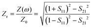 | (1) |
where S11 and S21 are reflection and transmission coefficients, respectively. The relationship between absorption (A), reflectance (R) and transmission (T) of a metamaterial absorber can be expressed as A = 1 − R − T. It is clear that a decrease in R and T is accompanied by an increase in absorption. And the expression for calculating reflection is:23| |  | (2) |
where Z(ω) and Z0 are the structure impedance and the free space impedance, respectively. Clearly, when the structural impedance and free space impedance of the absorber are equal, the reflection is minimised to zero. Whereas equal free space impedance and structural impedance means impedance is perfectly matched and vice versa is not perfectly matched. In addition, when the impedance is perfectly matched it also means that the normalised relative impedance is 1, i.e., the real part is close to 1 and the imaginary part is close to 0. Therefore, we can measure the impedance matching effect of the absorber by the normalized relative impedance.
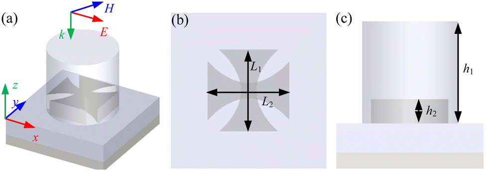
Firstly, we designed a fully dielectric narrow-band metamaterial absorber as shown in Fig. 1, which mainly consists of Si3N4 columns with Si3N4 substrate, and Ti reflective layer. The thickness of the Si3N4 substrate is 350 nm, and the thickness of the Ti reflective layer is 200 nm, which is greater than the skinning depth of the light, so the light cannot penetrate the reflective layer and its transmission is close to zero. The radius of the Si3N4 cylinder is R, and the height is h1. The FDTD method is used to analyse the absorption properties of the absorber, with a periodic boundary condition in the x, y direction, and a perfectly matched layer (PML) in the z direction. The FDTD simulation region is 1.45 μm in the x, y direction, 30 μm in the z direction and the mesh size is 6 nm. The refractive indices of Ti and Si3N4 are obtained respectively from the Palik24 and Kischka,25 respectively.
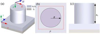 |
| | Fig. 1 (a) Schematic diagram, (b) top view, and (c) side view of the NMA. | |
3. Results and discussions
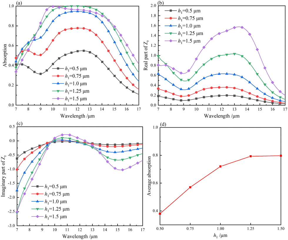
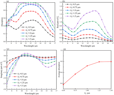
The absorption spectra of the narrowband metamaterial absorber in TM mode (electric field along x direction) as an incident light source for different height h1 are shown in Fig. 2a. When h1 < 1.25 μm, as the height h1 increases, the absorption gradually increases over the whole band (7–17 μm). When h1 > 1.25 μm, the height h1 continues to increase and the absorption of the absorber starts to decrease, especially in the 10–14 μm region. When h1 is 1.25 μm, the absorption of the absorber peaks at 99.9% and the absorption bandwidth with absorption greater than 90% is approximately 4.8 μm (9.5–14.3 μm). As shown in Fig. 2b and c, the trend of the relative impedance corresponds to the absorption spectrum, and as the height h1 increases, the real part of the relative impedance tends to 1 and the imaginary part tends to 0 in the range of 9.5–14.3 μm when h1 < 1.25 μm. And when h1 > 1.25 μm, the real and imaginary parts of the relative impedance start to shift, which also means that the impedance matching is not effective. The increase in height causes the structural impedance to increase in value and match the free space impedance, but when it reaches the peak value, the structural impedance continues to increase with the increase in height, resulting in impedance mismatch. In order to better evaluate the absorption performance of the absorber in the whole incident band, we use the average absorption rate as the evaluation index. The average absorption (Aaverage) is expressed as:  , where λ2 and λ1 are the maximum and minimum values of the incident source, respectively. Fig. 2d shows the average absorption spectra for different thicknesses of h1. Clearly, for h1 < 1.25 μm, the average absorption increases with increasing h1 throughout the incident band. However, for h1 greater than 1.25 μm, the average absorption does not change significantly across the band as h1 increases, which is also in better agreement with the absorption spectra. Therefore, the absorption is essentially optimal at h1 of 1.25 μm.
 |
| | Fig. 2 (a) Absorption spectra, (b) real part of Zr, (c) imaginary part of Zr for the UMA with different thickness h1, (d) average absorption spectra for different h1. | |
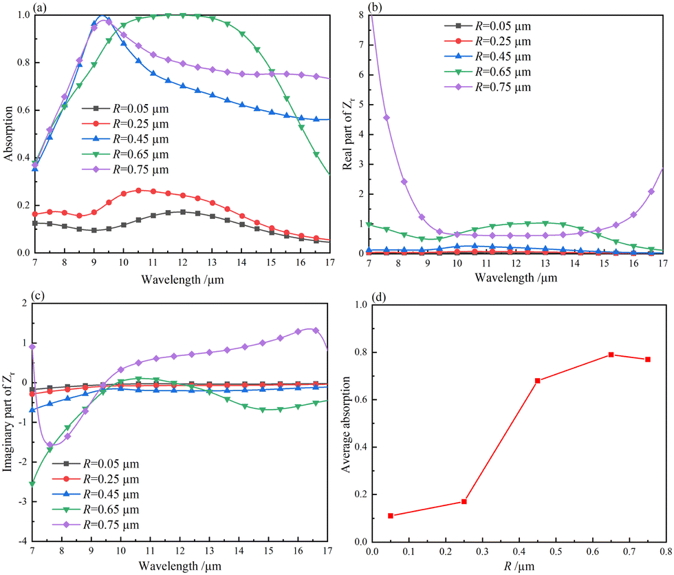
The R-dependent absorption spectrum is shown in Fig. 3a. It is clear that as R increases, the absorption of the metamaterial absorber also gradually increases in the whole band region when R < 0.45 μm. When R = 0.45 μm, the absorber has an absorption peak at 9 μm wavelength. And when R = 0.65 μm, the absorber has the best absorption performance. When R > 0.65 μm, the absorption performance of the absorber decreases and the absorption band becomes narrower. As shown in Fig. 3b and c, the real and imaginary curves of the relative impedance of the absorber show that the impedance matching is best when R is 0.65 μm, which is also related to the variation of the absorption spectrum (Fig. 3a).
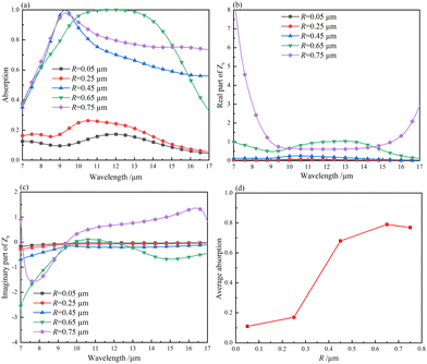 |
| | Fig. 3 (a) Absorption spectra, (b) real part of Zr, (c) imaginary part of Zr for the UMA with different radius R, (d) average absorption spectra for different R. | |
We have also calculated the average absorption for different radius R as shown in Fig. 3d. As the radius R increases, the average absorption of the absorber over the whole incident band also increases significantly when R < 0.65 μm. And when the radius R exceeds 0.65 μm, the average absorption decreases with increasing R, which is also consistent with the absorption and impedance spectrum analysis.
The above absorber uses Si3N4 to realise a fully dielectric metamaterial narrowband absorber. To further broaden the absorption bandwidth, hyperbolic rectangles are added to the Si3N4 substrate with the expectation that the introduction of resonant inductance, capacitance and resistance will alter the structural impedance of the absorber to achieve the best impedance matching effect. The schematic diagram of the ultra-wideband perfect absorber is shown in Fig. 4. The length of the hyperbolic rectangle is L1, L2, and the height is h2. The surface function for the horizontal (x-direction) hyperbolic rectangle is ±(x2 + 1) and the vertical (y-direction) hyperbolic rectangle is obtained by rotating the x-direction hyperbolic rectangle by 90°. The optimised structural parameters are: R = 0.65 μm, h1 = 1.25 μm, h2 = 0.3 μm, L1 = L2 = 1.05 μm.
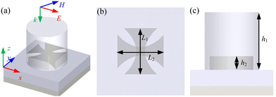 |
| | Fig. 4 (a) Schematic diagram, (b) top view, and (c) side view of the UMPA. | |
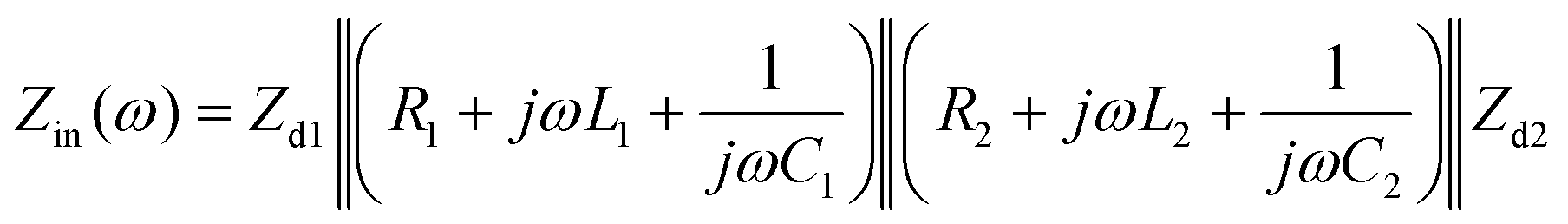
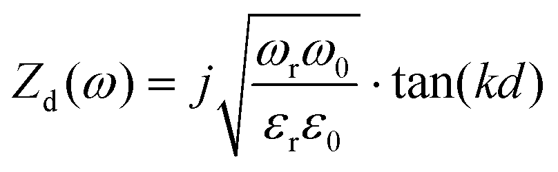
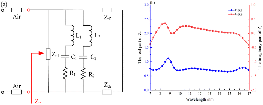
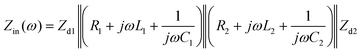
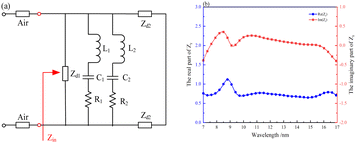
The equivalent circuit is shown in Fig. 5a. R is the intrinsic ohmic loss of the material. L, C are the equivalent inductance and capacitance of the structure in the presence of the incident light source. Zd1 and Zd2 are the impedances of h2 and Ti substrate, respectively. Clearly, the input impedance (structure impedance) Zin is expressed as:
| |  | (3) |
in which:
| |  | (4) |
| |  | (5) |
where
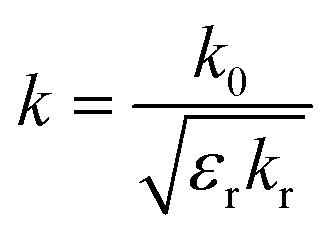
kr (or
k0),
εr (or
ε0) and
ωr (or
ω0) are the wave number, permeability, and relative permittivity of the dielectric layer (or free space). The structural impedance is mainly influenced by the presence of
R,
L,
C and
Zd, where
R is the ohmic loss of the material and is related to the intrinsic properties of the material. Therefore, the structural impedance can be adjusted by the shape and parameters of the structure to achieve a perfect impedance match. We calculate the relative impedance spectra of the UMPA as shown in
Fig. 5b. Clearly, the structural impedance of the absorber changes significantly with the addition of the Ti hyperbolic rectangles due to the introduction of component parameters such as resistance, inductance and capacitance into the circuit. From the relative impedance spectrum, the real part of the relative impedance is closer to 1 and the imaginary part is closer to 0 in the whole band region (7–17 μm), which also means that the introduction of the Ti structure can effectively improve the impedance matching effect and expand the absorber band.
 |
| | Fig. 5 (a) The equivalent circuit model, (b) relative impedance spectra. | |
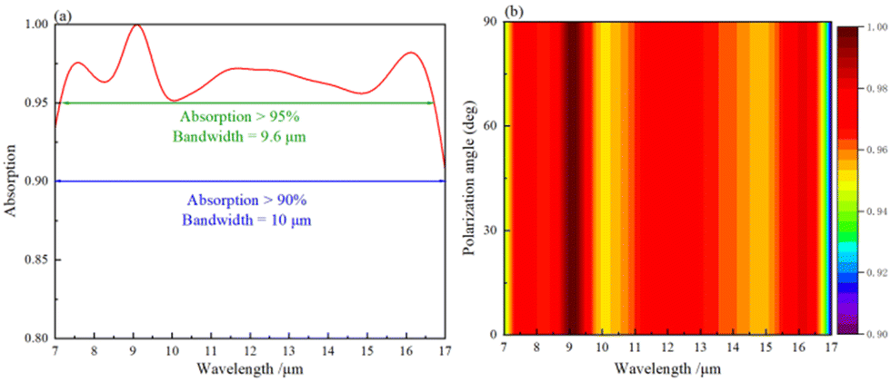
The absorption spectrum of the UMPA is shown in Fig. 6a, calculated with the structural parameters: R = 0.65 μm, h1 = 1.25 μm, h2 = 0.3 μm, L1 = L2 = 1.05 μm, and the light source is a plane wave in TM mode. Clearly, the absorption wavelength width of UMPA is 10 μm based on absorption >90%, and the absorption band region is 7 to 17 μm, which can completely cover the atmospheric transparency window. In addition, the absorption bandwidth of UMPA can reach 9.6 μm when calculated with absorption >95%, and the peak absorption of UMPA can reach 99.9%. UMPA has a good absorption characteristic with an average absorptivity of 96.6% over the band from 7 μm to 17 μm. In addition, to further verify the absorption properties of the UMPA, we calculated the absorption spectra at polarization angles of 0°–90°, as shown in Fig. 6b, with the geometrical parameters set unchanged. It is clear that as the polarization angle is changed, the absorption spectra remain unchanged. And the symmetry of UMPA in any direction makes its response the same in any direction, so the UMPA has polarization insensitive property.
 |
| | Fig. 6 (a) Absorption spectrum for UMPA, (b) absorption map for different polarization angles. | |
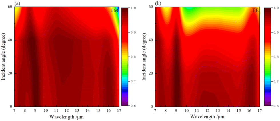
To further verify the wide-angle absorption characteristics of the UMPA, the absorption spectra of the absorber in the TM mode in the region of incidence angles of 0°–60° were calculated as shown in Fig. 7a, keeping other parameters constant. When the incident angle is less than 40°, the incident angle has a small effect on the UMPA absorption, and with increasing angle, the absorption is almost constant over the whole band region. On the other hand, when the angle of incidence is greater than 40°, the absorption decreases more significantly across the band as the angle of incidence increases. Nevertheless, the average absorption of UMPA can reach 88% when the angle of incidence is 60°. In addition, we also calculated the absorption spectra of the absorber in the TE mode (electric field along x direction) in the range of incident angles from 0° to 60°, as shown in Fig. 7b. It is obvious that the absorption rate remains almost constant with increasing angle when the angle of incidence is less than 20°. When the angle of incidence is greater than 20°, the absorption of UMPA shows a significant decrease with increasing angle over the whole band region (7–17 μm). Similarly, the average absorption of UMPA in TE mode can reach 78% at large angles (60°) of oblique incidence. Overall, UMPA has some wide angle absorption properties over the entire band range.
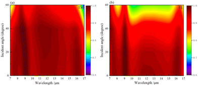 |
| | Fig. 7 (a) The absorption spectra at different incidence angles for the TM mode, (b) absorption spectra at different incidence angles for the TE mode. | |
In addition, to further validate the performance of the UMPA, we compare it with the reported work as shown in Table 1. It can be clearly seen that, the UMPA designed by us has wider absorption bandwidth and higher absorption. Besides this, the designed metamaterial absorber has a simple structure and easily accessible materials, which more favourable for integration and application.
Table 1 Comparing with the reported work
| Ref. |
Waveband (μm) |
Bandwidth (μm) |
Average absorption (%) |
Material |
|
18
|
6–16 |
6 |
— |
Ge/TiO2/Ti |
|
19
|
8–13 |
4.1 |
95 |
Al/Si |
|
20
|
8–14 |
4 |
86 |
Ti/Ge |
|
26
|
8–18 |
8 |
92.1 |
Ti/GaAs/Ge |
| This work |
7–17 |
10 |
96.6 |
Ti/Si3N4 |
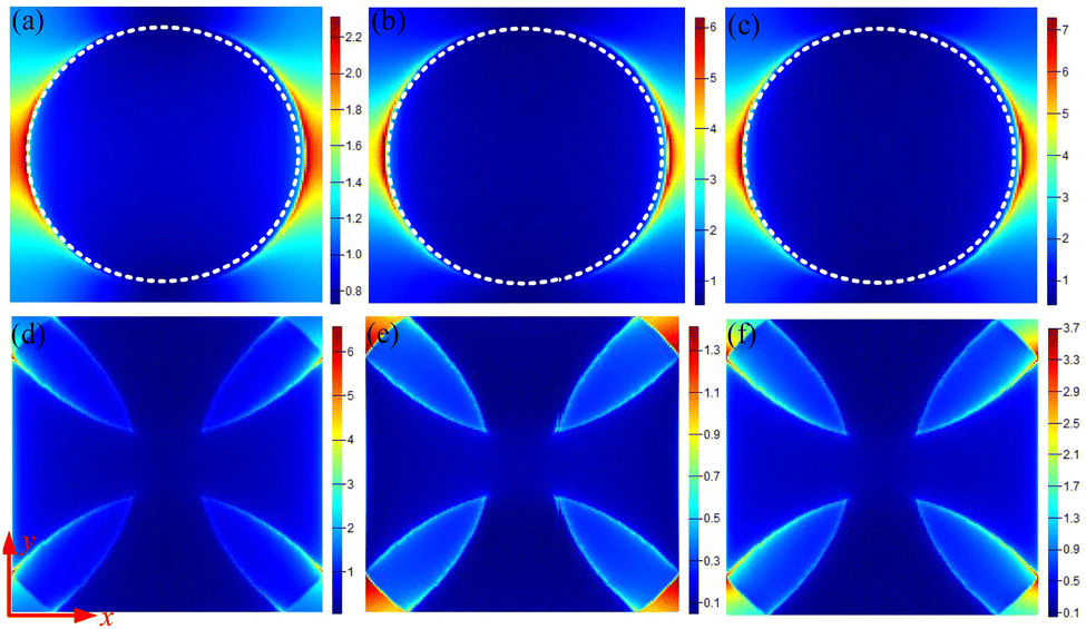
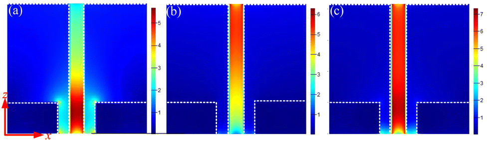
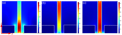
In order to reveal the mechanism of high efficiency and broadband formation of UMPA, the electric field distribution at the resonance wavelengths (9, 11.4, 16 μm) at different heights of the x–y plane (h1, h2) is shown in Fig. 8. As shown in Fig. 8a–c, the electric field distribution at the Si3N4 cylindrical surface (h1) shows that the electric field enhancement region is mainly concentrated at the slit adjacent to the cylinder, while the electric field at the Si3N4 surface is hardly significantly enhanced. As shown in Fig. 8d–f, the electric field distribution on the Ti hyperbolic rectangular surface (h2) shows that the electric field enhancement region is mainly concentrated at the surface corners and edges of the Ti rectangle. In addition, the electric field at the gap adjacent to the Si3N4 cylinder is also significantly enhanced. Comparison of the electric field distribution between the Si3N4 surface and the Ti surface shows that the electric field on the Ti surface is significantly higher than that on the Si3N4 surface (e.g., Fig. 8a and d). This is because Ti and Si3N4 form a metal–dielectric interface, and the surface plasmon resonance can be excited when the relative dielectric constants and magnetic dielectric constants of the two sides of the dielectric meet the momentum matching requirements. When there is a perpendicular incidence structure of the TM mode wave, the free electrons and the incident wave satisfy the resonance conditions to form the surface plasmon resonance (SPR),27,28 and the energy is bound on the metal surface at the time of resonance. The surface waves generated by the SPR are directed to the surface and corners to further confine the energy, resulting in a localized surface plasmon resonance (LSPR)29 and further enhancement of the electric field at the metal surface. In addition, the coupling between the LSPR and the cavity resonance at the gap between the periodic cells also widens the absorption bandwidth and increases the absorption rate.
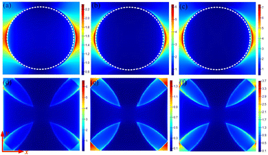 |
| | Fig. 8 (a)–(c) The electric field |E| distribution at the surface of height h1 in the x–y plane for wavelength of 9 μm, 11.4 μm, 16 μm, (d)–(f) the electric field |E| distribution at the surface of height h2 in the x–y plane for wavelength of 9 μm, 11.4 μm, 16 μm. | |
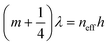
To further reveal the resonance modes at the gap between the periodic cells, the electric field distribution at different wavelengths (9, 11.4, 16 μm) is shown in Fig. 9, where the parameters are kept constant during the simulation. When the wavelength is 9 μm (Fig. 9a), the electric field enhancement region is mainly concentrated at the bottom of the central gap (air) between two periodic cells (Si3N4 cylinders). When the wavelength is 11.4 μm (Fig. 9b), the electric field enhancement region is mainly concentrated at the top of the gap between the periodic cells, and the enhancement strength is weaker compared to that of the wavelength of 9 μm. When the wavelength is 16 μm (Fig. 9c), the electric field enhancement region is mainly concentrated in the whole slit cavity, and the enhancement is stronger in the lower part than in the upper part. The TM mode wave is perpendicularly incident on the UMPA and is excited in the slit (air) cavity to produce cavity resonance. Cavity resonance creates standing waves so that the energy is highly localized and the electric field is greatly enhanced. This form of standing wave is similar to the standing wave produced by the Fabry–Perot resonance and the wavelengths of the F–P resonance in the TM mode are as follows:30
| |  | (6) |
| |  | (7) |
where
λ is the wavelength the wavelength of the F–P resonance,
h is the height of the Si
3N
4 cylinder,
neff is the effective refractive index calculated from
eqn (7), and
m is the cavity resonance mode order of the cavity.
εm and
εd are the relative permittivity of the metal and dielectric. The F–P resonance wavelength can be calculated from the formula to be about 9.04 μm, and the theoretical calculations are consistent with the results of the FDTD method, which also indicates that the enhancement of the electric field at the gap is mainly due to the F–P resonance. The F–P resonance mode generates a standing wave, which prolongs the time of interaction between the light and the structure, thus enhancing the absorption. And it can also be seen from the electric field distribution diagram that there is mutual coupling between the F–P resonance and the LSPR resonance on the Ti surface, which further enhances the absorption rate and bandwidth.
 |
| | Fig. 9 (a)–(c) The electric field |E| distribution in the x–z plane for wavelengths of 9 μm, 11.4 μm, 16 μm. | |
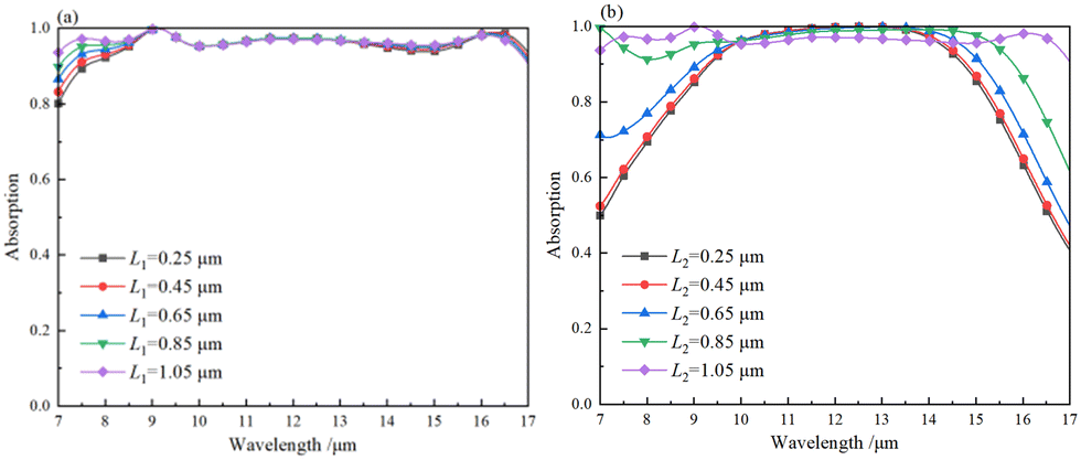
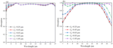
The adjustment of the absorption bandwidth of the absorber is further investigated. Keeping the other parameters constant, the L1 dependent effect on the UMPA absorption was calculated as shown in Fig. 10a. It is clear that the length L1 of the hyperbolic rectangle mainly affects the 7 μm to 9 μm band region, and as L1 increases, the absorber absorption in this band increases. In addition, we also calculated the effect of another hyperbolic rectangle length L2 on the absorber absorption, as shown in Fig. 10b. The effect of L2 on the absorptivity is small when L2 < 0.65 μm, when the absorption is mainly dominated by the Si3N4 column. When L2 > 0.65 μm, the absorption increases significantly across the band (7–17 μm) as the length of L2 increases, at which point the absorption is seen to be dominated by the Ti hyperbolic rectangle and the Si3N4 columns together. The best absorption performance of the UMPA is obtained when L2 = 1.05 μm.
 |
| | Fig. 10 (a) Absorption spectra of various L1, (b) absorption spectra of various L2. | |
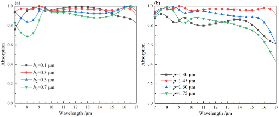
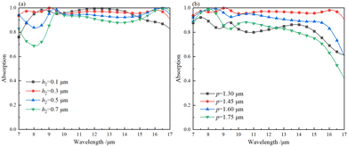
The absorption spectrum associated with the thickness h2 of the Ti hyperbolic rectangle is shown in Fig. 11a. When h2 < 0.3 μm, the absorbance gradually increases with increasing h2, particularly in the 7–9.5 μm band region, resulting in an increase in the absorption bandwidth of the absorber. When h2 > 0.3 μm, the absorbance gradually decreases with increasing h2 throughout the band, resulting in a narrower absorption band for the absorber. We also calculated the effect of period p on the absorption in a similar way, and the p-dependent absorption spectrum is shown in Fig. 11b. When p < 1.45 μm, the absorbance also increases significantly throughout the band with increasing wavelength. When p = 1.3 μm, the gap between the periodic units is small. Whilst one of the major contributions to the absorption of the absorber is the cavity resonance within the gap between the units, if the gap is too small, the cavity resonance cannot be excited and therefore the absorption is small at this point. When p > 1.45 μm, the absorption gradually decreases over the whole band (7–17 μm) as p increases. This is due to the fact that as p increases, the gap between the periodic units also increases, which affects the cavity resonance mode and intensity, and hence the absorption.
 |
| | Fig. 11 (a) Absorption spectra of various h2, (b) effect of the period p on absorption. | |
4. Conclusion
In this paper, we design an all-dielectric narrowband metamaterial absorber based on impedance matching theory combined with Si3N4 material. The absorption characteristics are analyzed using FDTD, which shows that the absorption rate of the narrow-band metamaterial absorber is more than 90% in the absorption band range from 9.5 μm to 14.3 μm, with an absorption bandwidth of 4.8 μm. The radius and thickness of the Si3N4 columns can be adjusted to match the absorption band range of the absorber. To further extend the absorption bandwidth, an ultra-broadband perfect metamaterial absorber is designed based on the narrowband absorber structure combined with impedance matching theory and equivalent circuit model. Numerical analysis shows that the absorption rate of the ultra-broadband perfect absorber is more than 90% in the band range from 7 μm to 17 μm, and the absorption peak value can reach 99.9%. When the absorption rate exceeds 95%, the absorption bandwidth of the UMPA can reach 9.6 μm, and it has polarization insensitivity and wide-angle absorption characteristics. The ultra-broadband and high absorption properties are mainly contributed by localized surface plasmon resonances, F–P resonances and inter-resonance interactions. The designed metamaterial absorber with high absorption, broadband, polarization insensitivity and wide-angle absorption characteristics has certain applications in energy harvesting and infrared sensing.
Conflicts of interest
There are no conflicts to declare.
Acknowledgements
The authors are grateful to the support by National Natural Science Foundation of China (61963016, 61967007, 62366015); Key Research and Development Program of Jiangxi Province (20201BBF61012); University Natural Science Foundation of Anhui Province (2022AH051578, 2023AH051543); Innovation and Entrepreneurship Training Programme for College Students in Anhui Province (S202210381009).
References
- Y. Zheng, Z. Yi and L. Liu,
et al., Numerical simulation of efficient solar absorbers and thermal emitters based on multilayer nanodisk arrays, Appl. Therm. Eng., 2023, 230, 120841 CrossRef CAS.
- R. Lai, P. Shi and Z. Yi,
et al., Triple-band surface plasmon resonance metamaterial absorber based on open-ended prohibited sign type monolayer graphene, Micromachines, 2023, 14(5), 953 CrossRef PubMed.
- S. Chen, H. Cheng and H. Yang,
et al., Polarization insensitive and omnidirectional broadband near perfect planar metamaterial absorber in the near infrared regime, Appl. Phys. Lett., 2011, 99(25), 253104 CrossRef.
- H. Zhang, Y. Cheng and F. Chen, Quad-band plasmonic perfect absorber using all-metal nanostructure metasurface for refractive index sensing, Optik, 2021, 229, 166300 CrossRef CAS.
- Y. Cheng, F. Chen and H. Luo, Plasmonic chiral metasurface absorber based on bilayer fourfold twisted semicircle nanostructure at optical frequency, Nanoscale Res. Lett., 2021, 16(1), 1–9 CrossRef PubMed.
- W. Wei, Q. Zhao and X. B. Shi, Preparation of gold nanoclusters by template method and applications in biomolecule biosensing, Acta Laser Biol. Sin., 2019, 28(4), 296–304 Search PubMed.
- J. Liu, W. Chen and W. Z. Ma,
et al., Ultra-broadband infrared absorbers using iron thin layers, IEEE Access, 2020, 8, 43407–43412 Search PubMed.
- Y. Zhang, Z. Yi and X. Wang,
et al., Dual band visible metamaterial absorbers based on four identical ring patches, Phys. E, 2021, 127, 114526 CrossRef CAS.
- N. I. Landy, S. Sajuyigbe and J. J. Mock,
et al., Perfect metamaterial absorber, Phys. Rev. Lett., 2008, 100(20), 207402 CrossRef CAS PubMed.
- S. K. Chamoli and W. Li, Visibly transparent multifunctional camouflage coating with efficient thermal management, Opt. Lett., 2023, 48(16), 4340–4343 CrossRef CAS PubMed.
- X. Liu, T. Starr and A. F. Starr,
et al., Infrared spatial and frequency selective metamaterial with near-unity absorbance, Phys. Rev. Lett., 2010, 104(20), 207403 CrossRef PubMed.
- J. Li, R. Gan and Q. Guo,
et al., Tailoring optical responses of infrared plasmonic metamaterial absorbers by optical phonons, Opt. Express, 2018, 26(13), 16769–16781 CrossRef CAS PubMed.
- L. He, Y. Yi and J. Zhang,
et al., A four-narrowband terahertz tunable absorber with perfect absorption and high sensitivity, Mater. Res. Bull., 2024, 170, 112572 CrossRef CAS.
- W. Lu, Z. Yi and J. Zhang,
et al., A tunable broadband absorber in the terahertz band based on the proportional structure of a single layer of graphene, Diamond Relat. Mater., 2023, 140, 110481 CrossRef CAS.
- R. Lai, H. Chen and Z. Zhou,
et al., Design of a penta-band graphene-based terahertz metamaterial absorber with fine sensing performance, Micromachines, 2023, 14(9), 1802 CrossRef PubMed.
- W. Li, F. Xu and S. Cheng,
et al., Six-band rotationally symmetric tunable absorption film based on alcufe quasicrystals, Opt. Laser Technol., 2024, 169, 110186 CrossRef CAS.
- Y. Zhu, J. Cheng and Z. Yi,
et al., Spectrally selective solar absorber and thermal infrared suppression based on hollow cylindrical microstructures, Opt. Commun., 2023, 549, 129910 CrossRef CAS.
- L. Sun, D. Liu, J. Su, X. Li, S. Zhou, K. Wang and Q. Zhang, Near Perfect Absorber for Long-Wave Infrared Based on Localized Surface Plasmon Resonance, Nanomaterials, 2022, 12(23), 4223 CrossRef CAS PubMed.
- K. Üstün and G. Turhan-Sayan, Ultra-broadband long-wavelength infrared metamaterial absorber based on a double-layer metasurface structure, JOSA B, 2017, 34(2), 456–462 CrossRef.
- E. Hou, Z. Liang and S. Zhang,
et al., Broadband metamaterial absorber based on hybrid multi-mode resonance in mid-wave and long-wave infrared region, Results Phys., 2022, 42, 105972 CrossRef.
- Y. Zhou, Z. Liang and Z. Qin,
et al., Small-sized long wavelength infrared absorber with perfect ultra-broadband absorptivity, Opt. Express, 2020, 28(2), 1279–1290 CrossRef CAS PubMed.
- F. Ding, J. Dai and Y. T. Chen,
et al., Broadband near-infrared metamaterial absorbers utilizing highly lossymetals, Sci. Rep., 2016, 6, 39445 CrossRef CAS PubMed.
- R. M. H. Bilal, M. A. Baqir and M. Hameed,
et al., Triangular metallic ring-shaped broadband polarization-insensitive and wide-angle metamaterial absorber for visible regime, JOSA A, 2022, 39(1), 136–142 CrossRef CAS PubMed.
-
E. D. Palik, Handbook of Optical Constants of Solids, Academic, 1985 Search PubMed.
- J. Kischkat, S. Peters and B. Gruska,
et al., Mid-infrared optical properties of thin films of aluminum oxide, titanium dioxide, silicon dioxide, aluminum nitride, and silicon nitride, Appl. Opt., 2012, 51(28), 6789–6798 CrossRef CAS PubMed.
- W. Zhang, M. Chao and Q. Liu,
et al., Broadband ultra-thin Long-Wave InfraRed metamaterial absorber based on trapezoidal pyramid array, Results Phys., 2023, 52, 106813 CrossRef.
- F. Zhou, F. Qin and Z. Yi,
et al., Ultra-wideband and wide-angle perfect solar energy absorber based on Ti nanorings surface plasmon resonance, Phys. Chem. Chem. Phys., 2021, 23(31), 17041–17048 RSC.
- F. Wu, P. Shi and Z. Yi,
et al., Ultra-broadband solar absorber and high-efficiency thermal emitter from UV to mid-infrared spectrum, Micromachines, 2023, 14(5), 985 CrossRef PubMed.
- Y. Wang, X. Xuan and S. Wu,
et al., Reverse design of metamaterial absorbers based on an equivalent circuit, Phys. Chem. Chem. Phys., 2022, 24(34), 20390–20399 RSC.
- D. R. Smith, W. J. Padilla and D. C. Vier,
et al., Composite medium with simultaneously negative permeability and permittivity, Phys. Rev. Lett., 2000, 84(18), 4184–4187 CrossRef CAS PubMed.
Footnote |
| † These authors contributed equally to this work and should be considered co-first authors. |
|
| This journal is © the Owner Societies 2024 |
Click here to see how this site uses Cookies. View our privacy policy here. 
 a,
Xiu
Li†
b,
Shenbing
Wu
a,
Changjun
Hu
a and
Yuanyuan
Liu
*c
a,
Xiu
Li†
b,
Shenbing
Wu
a,
Changjun
Hu
a and
Yuanyuan
Liu
*c

 , where λ2 and λ1 are the maximum and minimum values of the incident source, respectively. Fig. 2d shows the average absorption spectra for different thicknesses of h1. Clearly, for h1 < 1.25 μm, the average absorption increases with increasing h1 throughout the incident band. However, for h1 greater than 1.25 μm, the average absorption does not change significantly across the band as h1 increases, which is also in better agreement with the absorption spectra. Therefore, the absorption is essentially optimal at h1 of 1.25 μm.