
 Open Access Article
 This Open Access Article is licensed under a Creative Commons Attribution-Non Commercial 3.0 Unported Licence
Solution processed metal chalcogenide semiconductors for inorganic thin film photovoltaics
Jonathan W.
Turnley
 and
Rakesh
Agrawal
*
and
Rakesh
Agrawal
*
Davidson School of Chemical Engineering, Purdue University, West Lafayette, Indiana 47907, USA. E-mail: agrawalr@purdue.edu
First published on 29th April 2024
Abstract
Thin film photovoltaics are a key part of both current and future solar energy technologies and have been heavily reliant on metal chalcogenide semiconductors as the absorber layer. Developing solution processing methods to deposit metal chalcogenide semiconductors offers the promise of low-cost and high-throughput fabrication of thin film photovoltaics. In this review article we lay out the key chemistry and engineering that has propelled research on solution processing of metal chalcogenide semiconductors, focusing on Cu(In,Ga)(S,Se)2 as a model system. Further, we expand on how this methodology can be extended to other emerging metal chalcogenide materials like Cu2ZnSn(S,Se)4, copper pnictogen sulfides, and chalcogenide perovskites. Finally, we discuss future opportunities in this field of research, both considering fundamental and applied perspectives. Overall, this review can serve as a roadmap to researchers tackling challenges in solution processed metal chalcogenides to better accelerate progress on thin films photovoltaics and other semiconductor applications.
 Jonathan W. Turnley | Jonathan Turnley graduated from Presbyterian College in 2018 with BS degrees in Chemistry and Physics. In 2023 he completed his PhD in Chemical Engineering at Purdue University after studying the synthesis of metal chalcogenide semiconductors for photovoltaic applications. He is currently a postdoctoral research associate at University of Illinois Urbana-Champaign. |
 Rakesh Agrawal | Rakesh Agrawal is the Winthrop E. Stone Distinguished Professor in the Davidson School of Chemical Engineering at Purdue University. His research interests include solution processed inorganic solar cells, chemical separations, shale gas processing, biomass to chemicals and fuels, gas liquefaction, and energy systems analysis. He is a member of the U.S. National Academy of Engineering and a Fellow of the American Academy of Arts and Sciences, the National Academy of Inventors, and AIChE. He is a recipient of the US National Medal of Technology and Innovation. His chemical engineering degrees are from IIT Kanpur, University of Delaware, and MIT. |
Introduction
Due to the abundance of sunlight that reaches earth, solar energy is poised to be the foremost source of renewable energy, primarily through the use of solar panels or photovoltaics (PV).1 This technology has improved remarkably in the past couple of decades, both increasing in efficiency and decreasing in cost, making it commercially viable and one of the fasted growing forms of energy generation in the world.2 However, several challenges remain and need to be solved before PV technology can scale beyond terawatt production levels.In its current form, the PV market is primarily composed of single-junction PV, meaning devices that rely on a single absorber material to capture light.3 Within this technology, silicon, both in monocrystalline and polycrystalline forms, is the absorber layer in most commercial panels. However, a substantial fraction of commercial panels employ metal chalcogenide semiconductors as the absorber layer, mostly Cu(In,Ga)(S,Se)2 and CdTe. Further, the halide perovskites have seen tremendous success in research labs and seem poised to make the jump to the commercial market in the coming years.2,3
While the PV market is growing quickly, it is still a relatively small part of the current energy sector.4 Therefore, it is important to consider how PV technology may need to change to meet global energy needs. Furthermore, with the ever-increasing threat of climate change, there is increasing pressure to make this transition to solar energy in as short a time period as possible.
It is highly likely that the future of PV technology will center on multi-junction photovoltaics.3 Unlike single-junction devices, multi-junction devices use multiple absorber materials with different bandgaps that are each optimized to better utilize different energies of light. Additionally, it is likely that innovation related to device fabrication will ultimately allow for production that is cheaper, faster, and consumes less energy.
Of particular promise are solution processing methods. Solution processing entails the deposition of materials out of a solution-based ink and can generally be done at ambient pressure and with low-to-moderate temperatures. While not used in large scale PV production today, solution processing could dramatically reduce the cost of PV production while also increasing throughput and more efficiently using precursor raw materials.5–8 From this perspective, it is then reasonable to question which, if any, of the current PV materials are positioned to meet all the needs of future solution-processed multi-junction photovoltaics.
A major benefit for silicon is that it is already in widespread use.3 This means there are significant production capacities in place and the industry has extensive experience in module production. Single-junction silicon PV has proven that it can achieve high performance and has the stability to last for decades in the field. Silicon is also an extremely abundant element and is generally non-toxic (Table 1). With a bandgap of around 1 eV, it is also well situated to be the bottom absorber in a tandem device.2 However, silicon also has several major drawbacks. First, it is an indirect bandgap material, meaning it has a relatively low absorption coefficient (around 102–103 cm−1 for the relevant photon wavelengths) and a thick layer greater than one hundred microns is needed to absorb all the incident sunlight.9 This is in contrast to the direct bandgap materials used in thin film solar cells where merely hundreds of nanometers or a few microns are needed to absorb all the sunlight. Furthermore, it is highly sensitive to defects and impurities, so careful processing with extremely high temperatures (over 1000 °C) is usually required to achieve the purity needed to produce a high performing PV module.2,10 The existing silicon PV infrastructure will likely result in its use in early multi-junction production.11 In the long-term, however, it is expected that all-thin-film multi-junction photovoltaics will be the primary technology, meaning that silicon will be replaced.3 This is especially true for a target of thin-film multijunction photovoltaics that are fully solution processed.
| Earth-abundant | Non-toxic | High solar cell performance | High stability | Solution processable | |
|---|---|---|---|---|---|
| Si | Yes | Yes | Yes | Yes | No |
| Halide perovskite | Yes | No | Yes | No | Yes |
| CdTe | No | No | Yes | Yes | Yes |
| Cu(In,Ga)(S,Se)2 | No | Yes | Yes | Yes | Yes |
| Ideal new material | Yes | Yes | Yes | Yes | Yes |
Organic–inorganic halide perovskites are situated as a near opposite of silicon (Table 1). Perhaps the most famous perovskite is methylammonium lead iodide, though this is really a class of materials with an ABX3 composition where A is a +1 cation, B is a +2 cation, and X is a −1 halide anion. The best performance is generally achieved by alloying methylammonium, formamidinium, and cesium at the A-site, lead and tin at the B-site, and iodine and bromine at the X-site. All of this alloying enables a tunable bandgap, though it is generally above 1.5 eV, positioning these materials as candidates for the top absorber in a tandem device.12 These halide perovskites have direct bandgaps and exceptionally high absorption coefficients (around 105 cm−1 for the relevant photon wavelengths), so a layer of only a few hundred nanometers is sufficient to absorb all incident sunlight.9 Furthermore, they can be easily solution processed and exhibit excellent defect tolerance. The key weakness of halide perovskites has been their lack of stability. These materials can be sensitive to heat, moisture, oxygen, applied voltage, and even light, which is a major limitation.2 It should be noted that overcoming this instability has been a major focus of the research community and significant progress has been made.13–15 But it is not yet clear that these materials can match silicon in terms of stability. An additional worry is the use of highly toxic Pb which poses real health concerns and creates regulatorily hurdles.
Perhaps the best situated to balance the various needs for a solution-processed multi-junction PV future are the metal chalcogenide semiconductors. As the foremost examples, Cu(In,Ga)(S,Se)2 and CdTe have both achieved commercial success, can produce high efficiency devices (above 23% and 22% on the lab scale, respectively), and can last for decades in the field.16,17 Both are direct bandgap materials and can make use of thin films on the order of a few microns.17 Of these two, CdTe does face challenges of being composed of toxic cadmium and rare tellurium.18 This leaves Cu(In,Ga)(S,Se)2 as an intriguing option. Bandgap tuning can be achieved by changing the indium-to-gallium or sulfur-to-selenium ratios. At the CuInSe2 composition, the bandgap is around 1 eV and well situated as a bottom absorber in a tandem device. But for higher gallium and sulfur content the bandgap can be pushed to up to 1.5 eV (or more), ideal as a top absorber in a tandem architecture.19 Commercial Cu(In,Ga)(S,Se)2 modules are made by vacuum deposition, either by treating a stack of metal precursors in a chalcogen atmosphere or through reactive co-evaporation. However, there have been challenges in further scaling of these techniques.2 On the other hand, this class of materials can be solution processed, opening the door for high-throughput roll-to-roll production.5 And yet Cu(In,Ga)(S,Se)2 isn’t without its own drawbacks. While indium isn’t especially low in abundance, there is substantial competition for it. Similarly, gallium and selenium are not especially abundant.18
With this line of thinking, the Agrawal Solar Energy Research Group has focused its efforts on solution processing of metal chalcogenide semiconductors, focusing on both Cu(In,Ga)(S,Se)2 and emerging materials that may address needs not met by any of the established semiconductor materials. This review covers research into the solution processing of metal chalcogenide thin films, primarily with an eye towards application in solar cells and highlighting the contributions of the Agrawal research group among others. To do this, we start by using Cu(In,Ga)(S,Se)2 as a model class of materials to underline the process of fabricating solution-processed thin films. We then expand to cover research effort into solution processing of emerging metal chalcogenide semiconductors and follow with a discussion of the emerging and versatile amine–thiol chemistry as applied to the synthesis and alloying of sulfide and selenide semiconductors. Finally, we will highlight several key opportunities that could lead to breakthroughs for solution processed thin film devices.
Approaches for solution processing: Cu(In,Ga)(S,Se)2 as a model system
As an established material with a commercial impact, the Cu(In,Ga)(S,Se)2 material system has been studied extensively, including as part of research on solution processing methods. This makes the Cu(In,Ga)(S,Se)2 family of materials an ideal example for discussing solution-processed metal chalcogenides. Not only was Cu(In,Ga)(S,Se)2 the focus of some of the first solution processed thin film PV, but the methods developed for this class of materials have been highly influential in the development of many emerging metal chalcogenide materials.In this article, we will focus on solution processing methods that rely on a coating ink. This means that chemical bath deposition and electrodeposition, both solution-based methods where the substrate is submerged in a solution, are not covered.
Ink-based methods, expanded upon below, begin with an ink that contains the precursors needed to fabricate the targeted metal chalcogenide thin film (Fig. 1). These precursors could either be in the form of a soluble molecular precursor or a colloidal nanoparticle. The inks are then deposited onto the targeted substrate via casting, coating, or printing, with initial annealing to produce a nanocrystalline film. Next the films receive some form of treatment to induce the formation of large grains. Finally, the remaining layers needed to finish the device are deposited. The best Cu(In,Ga)(S,Se)2 devices obtained using different inks and coating methods are summarized in Table 2 and key features that contributed to their high efficiencies will be expanded upon in the subsequent discussion.
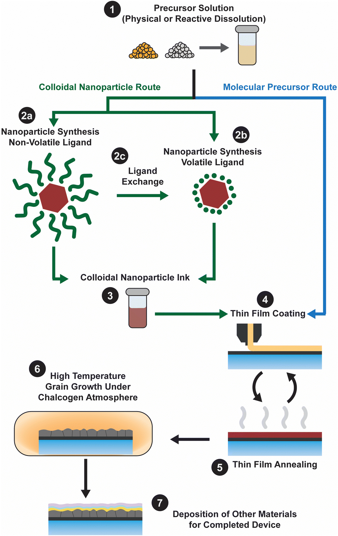 | ||
| Fig. 1 Fabrication scheme for solution processed absorber layer in thin film solar cells. | ||
| Ink Type | Coating method | Grain growth | Efficiency (%) | V oc (V) | J sc (mA cm−2) | FF (%) | Citation | |
|---|---|---|---|---|---|---|---|---|
| a Active area. b Total area. c Unspecified. | ||||||||
| Molecular precursor | Hydrazine–chalcogen | Spin coating | 540 °C | 15.2c | 0.623 | 32.6 | 75 | Todorov et al.22 |
| Hydrazine–chalcogen | Spin coating | 500–600 °C | 18.1a | 0.66 | 35.54 | 77.2 | Zhang et al.23 | |
| Amine–thiol | Spin coating | 550 °C with Se | 15.25a | 0.650 | 32.53 | 72.21 | Yuan et al.39 | |
| Amine–thiol | Spin coating | 550 °C with Se | 15.46a | 0.639 | 33.56 | 72.05 | Zhao et al.40 | |
| Amine–thiol | Spin coating | 520 °C with Se | 16.39a | 0.65 | 33.94 | 73.83 | Zhao et al.41 | |
| Amine–thiol | Spin coating | 550 °C with Se | 16.05a | 0.656 | 33.15 | 73.78 | Gao et al.86 | |
| Amine–thiol | Spin coating | 550 °C with Se | 16.02a | 0.656 | 33.61 | 72.65 | Zhao et al.88 | |
| DMF–thiourea | Spin coating | 580 °C with Se | 15.2a | 0.604 | 35.2 | 71.5 | Jiang et al.44 | |
| Ethanol–thiourea | Ink-jet printing | 530 °C with Se | 15.22b | 0.618 | 36.70 | 67.1 | Liu et al.45 | |
| Methanol (no chalcogen source) | Spin coating | 500 °C with H2S + Se | 15.3a | 0.612 | 34.1 | 73.1 | Kim et al.47 | |
| Methanol (no chalcogen source) | Spin coating | 500 °C with H2S + Se | 15.6a | 0.622 | 34.1 | 73.5 | Kim et al.48 | |
| Colloidal nanoparticle | Blade coating | 500 °C with Se | 15.0b | 0.63 | 32.1 | 73.4 | McLeod et al.62 | |
| Unspecified printing | Unspecified | 17.1c | 0.651 | 34.63 | 75.9 | Brown et al.72 | ||
| Spin coating and slot die coating | Unspecified temperature with Se | 18.68c | 0.660 | 37.2 | 76.0 | Aramoto et al.73 | ||
While this article is primarily focused on metal chalcogenide thin films for PV applications, these techniques can also find use in a variety of electronic and optoelectronic applications like transistors, light emitting diodes, and thermoelectrics.
Molecular precursor inks
Molecular precursor inks utilize soluble molecules that contain the target metal and chalcogen elements as precursors (Fig. 1 – step 1). After being coated at or near room temperature (Fig. 1 – step 4), heat treatment ideally leads to removal of the solvent and reaction of the precursors to produce the targeted metal chalcogenide thin film (Fig. 1 – step 5). Generally, the thin film is then heated in a chalcogen environment to coarsen the grains (Fig. 1 – step 6). For producing the highest quality thin film, chemistry of this ink should be carefully considered.The idea of molecular precursor deposition for a CuInSe2 solar cell can be traced back to aqueous spray coating of molecular precursor inks containing metal salts with thiourea or selenourea in 1979.20 However, molecular precursor inks based on hydrazine–chalcogen reactive dissolution chemistry really allowed for enhanced efficiencies approaching those obtained by vacuum deposition. This method was originally developed by Mitzi et al. at IBM, and efficiencies above 10% were achieved with inks containing Cu2S, In2Se3, Ga2Se3, S, and Se in hydrazine.21 Further optimization of this method and the use of Sb-doping resulted in efficiencies above 15%.22 Researchers from Raysoll Nanotech optimized the use of a Ga-gradient with this chemistry to achieve an efficiency of 18.1%.23
The power of the hydrazine–chalcogen method is its ability to minimize potential impurities in the resulting film. Hydrazine itself is made of only nitrogen and hydrogen atoms and can easily be volatilized or decomposed into gases. Additionally, in combination with a chalcogen, hydrazine has the ability to reactively dissolve a variety of generally insoluble metal chalcogenides via dimensional reduction.24 Dimensional reduction constitutes a 3D metal chalcogenide crystal structure being dismantled by reactive chalcogen species, forming lower dimensional units that are soluble in hydrazine. This reaction results in the formation of hydrazinium chalcogenidometallates which upon heating can cleanly decompose into the targeted metal chalcogenides.25 Working in a nitrogen-filled glovebox and avoiding metal salt precursors and organic solvents means that there is no source for potential oxygen, carbon, or halide impurities. However, there are significant safety concerns related to the use of hydrazine which is both highly toxic and explosive. These safety concerns create additional challenges for using this chemistry at an industrial scale.
As an alternative reactive dissolution chemistry, the Agrawal group has extensively studied the amine–thiol solvent system. Amine–thiol dissolutions were first independently reported by several groups. In early 2012, Liu et al. published that selenium could be dissolved in solutions of oleylamine and dodecanethiol.26 Around the same time, the Agrawal group reported that excess Se could be removed from Cu(In,Ga)Se2 nanoparticle syntheses by dissolution in a combination of oleylamine and hexanethiol.27 Then in 2013, Webber and Brutchey showed that solutions of 1,2-ethanedithiol and 1,2-ethylenediamine could reactively dissolve V2VI3 chalcogenides and appropriately termed amine–thiol solutions as alkahests. While the term “alkahest” dates back to alchemy and a search for a universal solvent, it has recently reemerged in a scientific context to describe solvent systems that are capable of solubilizing generally insoluble compounds via reactive dissolution (alkahest chemistry will be discussed in greater detail in subsequent sections). Within a short period, the Agrawal group showed that amine–thiol solutions could also reactively dissolve pure metals such as Cu, In, Ga, Zn, and Sn, and many of their sulfides and selenides.28–30 By adjusting the combination of amine and thiol, the reactivity of this system can be tuned, and researchers have found that over 100 precursors have been reactively dissolved.31 Similar to the hydrazine–chalcogen chemistry, reactive dissolutions of metal, chalcogen, and metal chalcogenide precursors can prevent incorporation of anionic impurities.
The Agrawal group has identified the metal thiolates formed from amine–thiol reactive dissolutions (Fig. 2a) and their decomposition mechanism into metal sulfides upon heating (Fig. 2b).28,32,33 It should be noted that the decomposition also produces other organic byproducts which are volatile, thereby minimizing impurities. With the ability to dissolve metal selenides and selenium, depending on precursor choice, this chemistry can enable to deposition of the sulfide Cu(In,Ga)S2 or the sulfoselenide Cu(In,Ga)(S,Se)2 material. While not always investigated in detail in the literature, it is important to note that evidence suggests even when making an ink from metal selenides and selenium the thiols present in the ink act as a sulfur source and produce Cu(In,Ga)(S,Se)2 rather than the pure selenide Cu(In,Ga)Se2.34 Recently, Turnley et al. introduced a sulfur-free, selenium-based alkahest using n-alkylammonium polyselenide solutions and reported CuInSe2 and Cu(In,Ga)Se2 absorber films without any fine grain layers.35 Preliminary CuInSe2 devices with minimal optimization showed efficiencies up to 7.25% and the potential for improvements is great due to the absence of impurities.
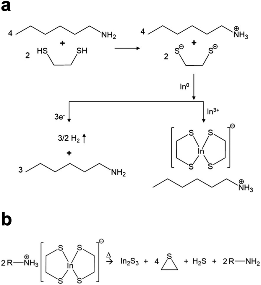 | ||
| Fig. 2 (a) Reactive dissolution mechanism for amine–thiol reaction with indium metal. Reprinted with permission.28 Copyright 2019 American Chemical Society. (b) Decomposition mechanism of the resulting indium thiolate into indium sulfide. Reprinted with permission.32 Copyright 2019 American Chemical Society. | ||
Amine–thiol chemistry has been used to great success for Cu(In,Ga)(S,Se)2 solar cells. The Agrawal group first used propylamine–ethanedithiol inks containing Cu2Se, In(III) acetate, Ga(III) acetylacetonate, and Se to produce devices with efficiencies above 12% and ultrathin devices (absorber layer ∼600 nm) with efficiencies above 10%.36 Later, in moving away from metal salt precursors, inks made from butylamine–ethanedithiol dissolutions of Cu2S, In, and Ga were used to obtain devices with active area efficiencies above 14%, among the highest efficiencies for devices without a gallium gradient.34 The group of Sixin Wu has also contributed substantially to amine–thiol processed Cu(In,Ga)(S,Se)2 devices. They first used inks of Cu, In, Ga, and Se dissolved in ethylenediamine–ethanedithiol solutions to produce 9.5% efficient solar cells.37 They later improved the efficiency to around 13% and then above 15% by employing strategies used in vacuum-deposited Cu(In,Ga)(S,Se)2 such as a Ga-gradient, surface sulfurization, and Ag-alloying.38–40 By controlling interfacial properties through the presence of the ordered vacancy compound they achieved an efficiency as high as 16.4%.41
While not explosive like hydrazine, amine–thiol chemistry does have safety concerns, especially from the use of toxic and malodorous thiols. One option that may help to alleviate these concerns is the separation of the synthesized alkylammonium metal thiolates from the bulk amine–thiol solution. Once separated, these metal organics can then be dissolved in a more benign solvent. Zhao et al. utilized this approach with redissolution in dimethyl sulfoxide (DMSO) and achieved around 9% efficient Cu(In,Ga)(S,Se)2 devices.28
On the other hand, in the pursuit of low-toxicity molecular precursor chemistry, researchers have devoted effort to improving inks based on polar organic solvent with a chalcogenourea. Solvents like DMSO and dimethylformamide (DMF) are substantially less toxic than hydrazine, ethylenediamine, and ethanedithiol.5 And the relatively polar nature of these solvents can allow some solubility of many common metal salts. Further, the solubility can be substantially increased with the addition of a complexing ligand. As a key step in the chemistry of this ink, thiourea and selenourea serve as an adduct on the metal salts, enhancing solubility and acting as the chalcogen source.42 The Hillhouse group applied this ink chemistry to Cu(In,Ga)(S,Se)2 solar cells, first achieving an efficiency of 14.7%.42 They also focused on the solution-processed gallium-free CuIn(S,Se)2 for tandem applications and produced efficiencies above 13%.42,43 Meanwhile, Jiang et al. used DMF–thiourea inks with CuCl, InCl3·4H2O, and GaCl3 to reach an efficiency of 15.2%.44 Liu et al. used an ethanol–thiourea ink with an additional ionic liquid and inkjet printing to produce Cu(In,Ga)(S,Se)2 devices above 15%.45 As a derivative of this method, SeCl4 has also been used as a chalcogen source that can also enhance the solubility of metal salts in DMF.46 Notably, researchers have also used methanol inks without a sulfur source to make oxide precursor films and were still able to achieve reasonably good efficiencies after selenization.47,48
Colloidal nanoparticle inks
Colloidal nanoparticle inks are attractive in that, unlike molecular precursor inks, the coating and the nucleation of nanocrystals are decoupled, giving additional degrees of freedom in designing processing conditions. Additionally, under ideal conditions exceptionally high mass concentrations can be achieved in colloidal nanoparticle inks. However, the differences between colloidal nanoparticle inks and molecular precursor inks also leads to new challenges. Of particular importance is nanoparticle ligand chemistry as surface ligand play important roles in controlling growth during synthesis and inducing colloidal stability in the ink.49 Unfortunately, these ligands can also introduce impurities into the resulting thin film.While colloidal nanoparticle synthesis has a long and celebrated history, much of it focused on metallic or binary chalcogenides materials like Au, Ag, Cu, CdS, CdSe, PbS, and PbSe.50–52 Synthesis of nanoparticles in the Cu(In,Ga)(S,Se)2 system posed a new challenge with its more complex crystal structure and frequent use of alloying (Fig. 1 – step 2). Early attempts to synthesize these materials showed challenges in obtaining a crystalline product, preventing agglomeration, and controlling formation of the chalcopyrite (tetragonal) phase versus the metastable sphalerite (cubic) phase.53–55 In 2008, results from the Agrawal and Hillhouse collaboration at Purdue University showed how reaction type can lead to phase control of CuInSe2, where sphalerite nanoparticles were obtained when Se was hot-injected into the reaction vessel containing CuCl and InCl3 and oleylamine but chalcopyrite nanoparticles are formed if the selenium is heated up with the CuCl and InCl3 in oleylamine.56 Furthermore, the nanoparticle shape can be changed with ligand chemistry, as the dual use of oleylamine and trioctylphosphine produced nanorings (Fig. 3).56 The Purdue team later studied the formation mechanism of these ternary nanoparticles, and hypothesized a binary-mediated route where depending on reaction conditions CuSe, Cu2−xSe, InSe, or In2Se3 will precede the formation of CuInSe2.57
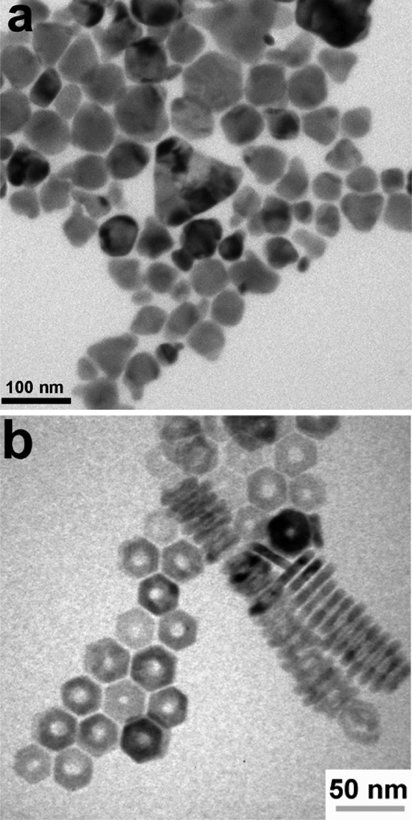 | ||
| Fig. 3 (a) Nanoparticles and (b) nanorings of CuInSe2 with morphology controlled by reaction conditions. Reprinted with permission.56 Copyright 2008 American Chemical Society. | ||
The application of nanoparticles for Cu(In,Ga)(S,Se)2 solar cells was first shown by the Purdue team, with CuInSe2 devices obtaining efficiencies up to 3.2%.56 The Korgel group published on this topic shortly after, though only obtaining efficiencies as high as 0.2%.58 A notable distinction in these methods is likely the cause for the efficiency difference. While the Korgel group stuck to low temperature processing and used a nanocrystalline absorber in the final device, the Purdue team used a moderate temperature heat treatment in the presence of selenium vapor to induce grain growth.56,58 At the time, a major impediment to achieving high efficiencies was that simply heating the selenide nanoparticle films at temperatures greater than 500 °C did not lead to coarsening into micron-sized grains. A major step forward in achieving high efficiencies came from the Purdue team when they introduced the selenization of sulfide nanoparticles as a means to coarsen grains and provide a dense selenide film.59,60 For Cu(In,Ga)S2 nanoparticle films, heating in a selenium atmosphere at temperatures of 500 °C or greater removed more than 95% of the sulfur in the material and resulted in dense Cu(In,Ga)(S,Se)2 absorber films. As such, it became common in the literature for sulfide precursors to be deposited and subsequently converted into coarse grain chalcogenide semiconductor films during a selenization process. Larger grain sizes reduce the number of interfaces in the film, which are known to be areas of high carrier recombination, improving the optoelectronic properties of the absorber layer. By optimizing the coating and grain-growth methods and taking advantage of sodium-inclusion, the use of sulfide Cu(In,Ga)S2 nanoparticles as precursors for a Cu(In,Ga)(S,Se)2 solar cell enabled the Purdue team to achieve efficiencies up to 12%.61 Later through further process optimization, the Agrawal group achieved total area efficiencies of 15% (active area efficiency of 16.2%).62 One of the reasons for this jump in efficiency past 12% might have been due to the use of KCN etching following coating. This step was employed with the intent of removing any CuSe from the precursor film before selenization. However, a second effect could have been the incorporation of potassium into the film, which is known to impact film morphology and device performance.63
Despite all of this progress in efficiency, large organic ligands (most commonly oleylamine) were used to cap the nanoparticles (Fig. 1 – step 2a). And these ligands contributed to a substantial amount of carbon impurities in the devices. Therefore, researchers have studied methods to replace these large organic ligands with smaller organic or inorganic ligands (through a process called ligand exchange, Fig. 1 – step 2c) or to use these smaller organic or inorganic ligands straight from the synthesis (Fig. 1 – step 2b).
As with many topics in Cu(In,Ga)(S,Se)2 nanoparticle research, ligand exchange chemistry was first studied extensively with cadmium and lead chalcogenide nanoparticles as simpler model systems.49,64 Ligand exchanges are often done in a single phase or in a two phase exchange. In the single phase, the nanoparticles are suspended in a solution with the target ligand. If the target ligand preferentially binds to the nanoparticle surface, over time it will replace the former ligand. On the other hand, in a two-phase system the target ligand and the nanoparticles are in two immiscible solvents (Fig. 4a). At the interface between the layers, nanoparticles can undergo ligand exchange and transfer to the other solvent, separating them spatially from the original ligand. The more complex surface of a ternary nanoparticle adds additional challenges in understanding and controlling ligands. One additional wrinkle in these exchanges is that amines, including oleylamine as the most commonly used ligand in these syntheses, has been observed to bind surprisingly strongly to the surface of CuInS2 nanoparticles.65 Therefore, ligand exchange methods must be carefully designed to obtain a higher percent removal of the oleylamine ligands.
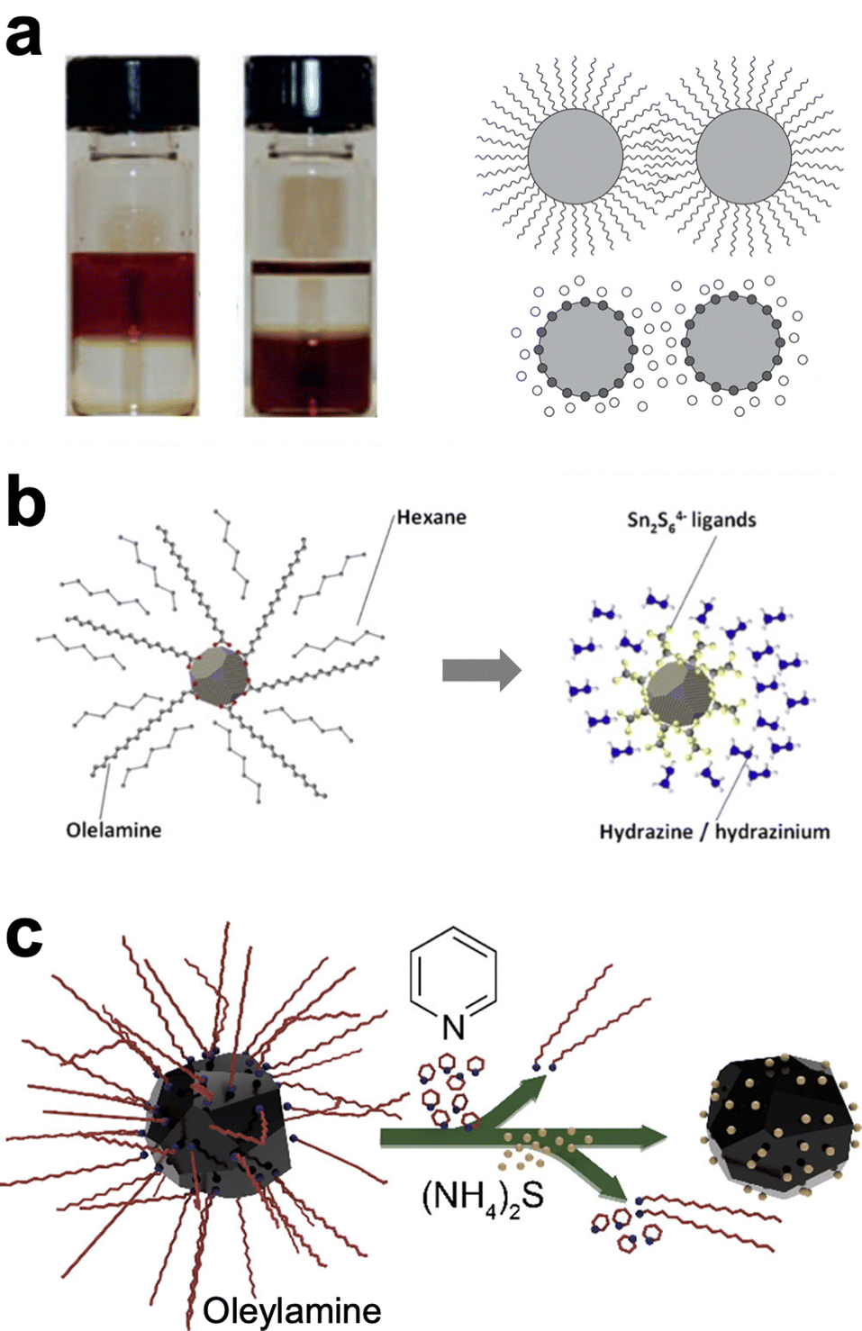 | ||
| Fig. 4 (a) Photograph and schematic of traditional, two-phase ligand exchange. Reprinted with permission.49 Copyright 2016 Springer Nature Limited. (b) Schematic of ligand exchange with inorganic, hydrazine-derived ligands. Reprinted with permission.68 Copyright 2012 Elsevier. (c) Schematic of hybrid, multistep ligand exchange. Reprinted with permission.69 Copyright 2020 American Chemical Society. | ||
One popular option has been to exchange for small inorganic ligands referred to as metal chalcogen complexes (MCCs).66–68 These MCCs are essentially the same chalcogenidometallates from hydrazine–chalcogen dissolution discussed above (Fig. 4b). Given the success and hazards of hydrazine–chalcogen molecular precursor chemistry, using these methods for nanoparticle ligands may not deliver a substantial enough benefit to justify the new safety concerns it introduces. The Agrawal group has targeted diammonium sulfide as an alternative inorganic ligand. Using a two-step exchange procedure (Fig. 4c), where oleylamine was first partially exchanged for pyridine and then exchanged for diammonium sulfide, over 98% of the oleylamine ligands could be removed and devices from these nanoparticles could achieve efficiencies up to 12%.69
To bypass the additional steps that ligand exchange introduces, direct synthesis of CuInS2 nanoparticles with small ligands has also been studied by the Agrawal group. To do this, metal thiolate molecules were heated in a sulfolane solution containing thioacetamide. During the heat up, the metal thiolates decompose into CuInS2 nanoparticles. The thioacetamide can also decompose, releasing H2S which can generate HS− ligands for the nanoparticles.70 With a similar motivation, CuInS2 nanoparticles were synthesized with a mixture of N-methyl-2-pyrrolidone (NMP) and propylamine ligands to reduce carbon impurities in the final CuInSe2 devices.71
Two of the highest efficiency solution processed Cu(In,Ga)(S,Se)2 solar cells have been reported by Nanosolar (17.1%) and Solar Frontier (18.7%), however less detail has been released about the fabrication methods.72,73 At least for the case of the Nanosolar device, it is known that a nanoparticle ink was used to print the absorber layer.72 For the Solar Frontier device, they report using a DMSO-based ink containing metal chalcogenides, which is most easily interpreted as a nanoparticle ink (though an interpretation of using some sort of molecular precursor metal chalcogen complex is also reasonable).73 Either way, these results exemplify the great potential for solution processing in the area of solar energy.
Thin film coating, grain growth, and film processing
Once a desired ink is obtained, the next step in the process is to deposit that ink onto the targeted substrate (Fig. 1 – step 4). This deposition process can play a major role in the quality of the resulting film and a variety of casting, coating, and printing techniques have been developed for this purpose. Techniques like spin coating, blade coating, slot-die coating, spray coating, and ink-jet printing have been developed to enhance the overall film quality. These deposition techniques are often combined with a low-to-moderate temperature annealing step in the range of 150 °C to 350 °C that results in a nanoparticulate film (Fig. 1 – step 5). While spin coating has been used extensively for lab-scale devices, Ellis et al. recently reported Cu(In,Ga)(S,Se)2 solar cells using slot die coating as a technique that could be more easily scaled to an industrial level.74,75 When carefully controlled and optimized, any of these techniques can result in extremely smooth films with controlled thicknesses ranging from a few nanometers to several microns. Fig. 5a and b show the top and cross-section scanning electron microscope (SEM) images of a film that was spin coated and annealed at 250–300 °C from a molecular precursor ink prepared by dissolving Cu2Se, indium acetate, and gallium acetylacetonate in a hexylamine–ethanedithiol (vol![[thin space (1/6-em)]](https://www.rsc.org/images/entities/char_2009.gif) :vol = 10:1) solution.36 The annealed film is very smooth and uniform, consisting of in situ formed nanocrystals with domain sizes less than 5 nm.76
:vol = 10:1) solution.36 The annealed film is very smooth and uniform, consisting of in situ formed nanocrystals with domain sizes less than 5 nm.76
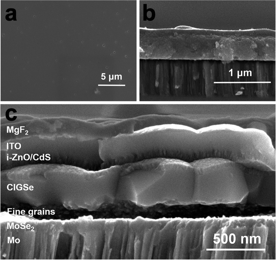 | ||
| Fig. 5 (a) Top view and (b) side view SEM images of nanoparticulate Cu(In,Ga)S2 precursor film and (c) side view SEM image of coarsened Cu(In,Ga)(S,Se)2 absorber in a completed device. Reprinted with permission.36 Copyright 2016 Royal Society of Chemistry. | ||
Ultimately, for a high-performance thin film solar cell, large grains are wanted to minimize the number of interfaces that carriers must cross within the absorber layer. Therefore, post-processing steps to induce grain growth in the nanoparticulate annealed films are often included in the solution processing of Cu(In,Ga)(S,Se)2 (Fig. 1 – step 6). In addition to inducing grain growth, this step in the process is likely to determine other factors like defect concentrations, grain boundary compositions, and surface properties. Therefore, this is a key step in obtaining high efficiency solar cells.
Initially, Guo et al. speculated that the coarsening of the sulfide Cu(In,Ga)S2 nanoparticles could be due to the larger lattice of the selenide crystal structure compared to the sulfide crystal structure.60 However, later work instead showed that liquid selenium condenses on the film and acts as a liquid flux, dissolving the precursor film and recrystallizing the large-grain selenide absorber.77,78 One major drawback for this process is the formation of a “fine-grain layer.” Instead of fully coarsening, it is common for a layer of smaller grains to be present, often at the bottom of the film. This fine-grain layer is often rich in carbon impurities. The presence of this layer has raised concerns on how it might impact device performance.34 To minimize the size of this layer, many researchers use thinner films overall, generally less than 1.5 μm despite high efficiency vacuum deposited Cu(In,Ga)(S,Se)2 using films of 2–3 μm in thickness. Fig. 5c shows the cross section SEM image of a Cu(In,Ga)(S,Se)2 solar cell prepared by the amine–thiol method described for Fig. 5a and b. A carbon and copper rich fine grain layer can be seen at the bottom of the coarsened absorber layer.
The selenium-flux mechanism also proposes an explanation for fine-grain layer formation.78 During this process, selenium condenses on top of the film and works its way down into the film leading to top-down coarsening. As this happens the metal sulfide precursors are dissolved into the liquid flux and the carbon impurities are rejected. As the growth works further down into the film, the carbon content continues to accumulate below the growth, eventually reaching a critical amount that stops further growth (Fig. 6).78
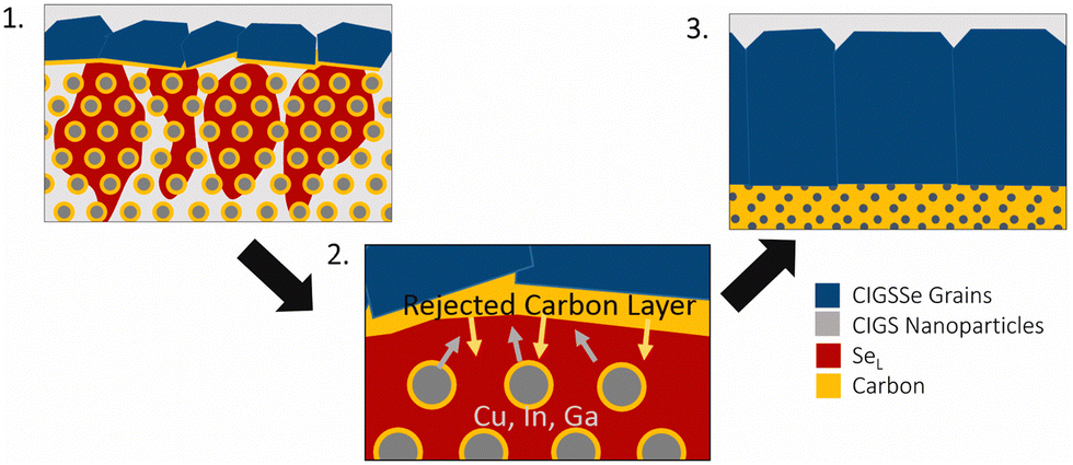 | ||
| Fig. 6 Schematic of grain growth mechanism and fine-grain layer formation via liquid selenium flux mechanism. Reprinted with permission.78 Copyright 2019 Elsevier. | ||
As such, one strategy to eliminate fine-grain layer has been to reduce the amount of carbon impurities in the film. Ellis et al. addressed this through ligand exchange on Cu(In,Ga)S2 nanoparticles to replace organic oleylamine ligands with inorganic diammonium sulfide ligands.69 By removing over 98% of the original oleylamine ligands, carbon impurities were dramatically reduced, and grain growth was enhanced. However, the fine-grain layer was not completely eliminated. A much thinner fine-grain layer was observed at the back of the absorber layer, but instead of being carbon-rich it was rich in copper and selenium.69 The Cu(In,Ga)(S,Se)2 family of materials is known to tolerate significantly off-stoichiometric compositions, particularly for copper content. So, the Agrawal group hypothesized that during the grain growth process, differences in reaction and diffusion rates between the different metals led to changes in the stoichiometry of the large-grain material, ultimately resulting in a small amount of copper and selenium rich material to form the fine-grain layer.
This then leads to the conclusion that to coarsen grains without a fine-grain layer, solution deposition routes need to both eliminate carbon impurities and have careful control over the chalcogen content. The Agrawal group addressed this in Deshmukh et al. where amine–thiol molecular precursor inks were tuned to utilize metal selenide precursors with excess elemental selenium to obtain films low in sulfur and carbon.34,79 Indeed, this allowed for coarsening without a fine grain layer. Turnley et al. further tuned the ink chemistry, eliminating the thiol as a potential sulfur and carbon source to confirm this result.35,79 In Deshmukh et al. and Turnley et al., films were able to fully coarsen at thicknesses greater than 2 μm (Fig. 7), something not previously shown in solution processed Cu(In,Ga)(S,Se)2 solar cells but standard in vacuum-deposited Cu(In,Ga)(S,Se)2 PV.34 However, there are still challenges with this process as the enhanced morphology in these films did not result in enhanced performance. More work is needed to better understand how to control defects, grain-boundaries, and interfaces to reach the potential of thicker films in solution processed Cu(In,Ga)(S,Se)2 PV.
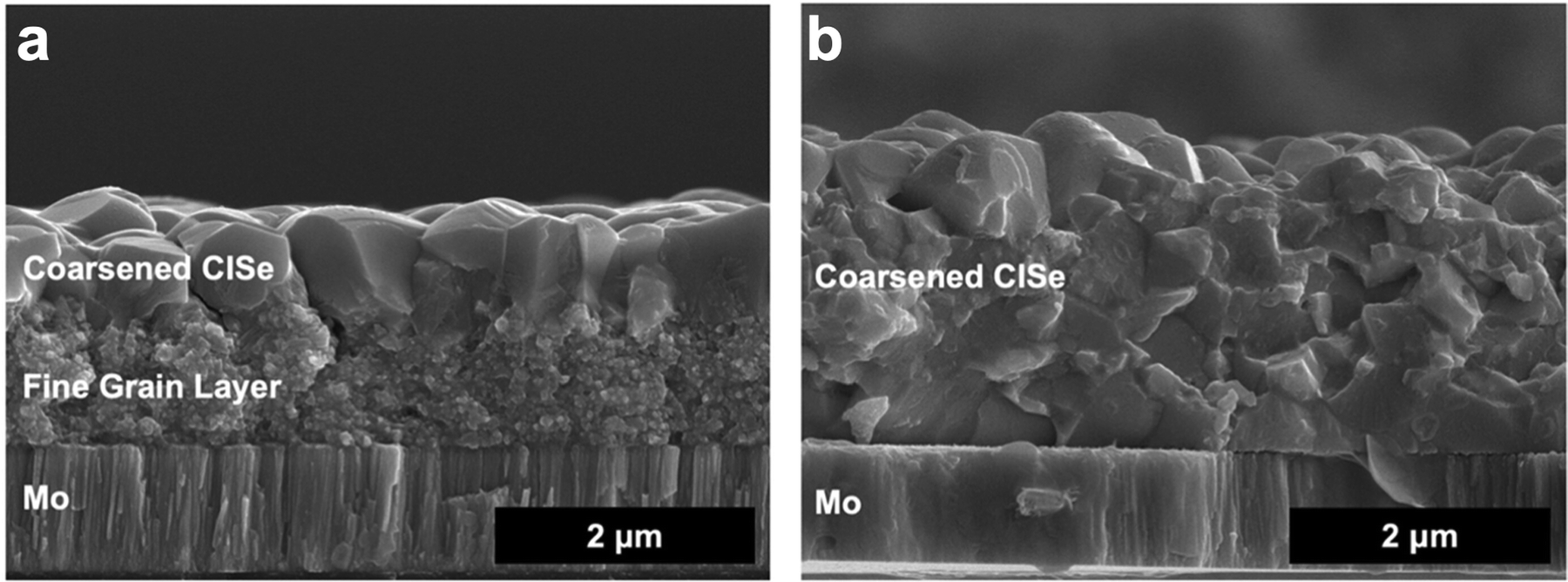 | ||
| Fig. 7 (a) SEM of coarsened CuInSe2 film made from a thick CuInS2 precursor film showing a large fine grain layer and (b) SEM of coarsened CuInSe2 film made from a thick CuInSe2 precursor film with no fine grain layer. Reprinted with permission.79 Copyright 2023 American Chemical Society. | ||
Beyond the use of selenium as a liquid flux, several other fluxing agents, based on both intrinsic and extrinsic elements, have been targeted for use in grain growth of solution processed Cu(In,Ga)(S,Se)2 solar cells. Considering elements that are intrinsic to the Cu(In,Ga)(S,Se)2 material system, in addition to elemental Se, CuSe is a common liquid fluxing agent.80 Given that the melting temperature is reported as 523 °C, a copper selenide complex flux is accessible within the normal processing temperature range for this material system of 500–600 °C. There is also the additional benefit that no extrinsic impurities are introduced that could hurt the optoelectronic properties. In terms of extrinsic fluxes, sodium polyselenides (Na2Sex) are another option that have been used to induce grain growth in solution processed Cu(In,Ga)(S,Se)2.81 Sodium has a long and complicated history as part of Cu(In,Ga)(S,Se)2. It is commonly incorporated during the growth process, either diffusing from the glass into the absorber material or being introduced intentionally. Depending on how and in what quantity the sodium is introduced, it can have beneficial or detrimental effects on the final material.7 Bismuth is another extrinsic element that has introduced to aid in grain through a proposed low melting point copper bismuth selenide.82
With any of these grain growth processes, it is important to keep in mind that at elevated temperatures and in the presence of a liquid flux, the atoms composing the Cu(In,Ga)(S,Se)2 can have a high mobility. This can lead to the loss of intentional compositional gradients (as discussed below, gallium grading and surface sulfurization can improve device performance) or the formation of undesired secondary phases.
High-performing solution-processed Cu(In,Ga)(S,Se)2 devices
In addition to the processing steps discussed above, a number of specific strategies are employed to boost efficiency in solution-deposited Cu(In,Ga)(S,Se)2. In general, many of these strategies are inspired by high-performing vacuum-deposited Cu(In,Ga)(S,Se)2. But modifications are needed to make these strategies applicable to solution processing. Analysis of the solution processed devices that have achieved efficiencies above 15% (Table 2) can convey which of these strategies have been most successful to date. For future progress towards 20% efficient solution processed Cu(In,Ga)(S,Se)2 solar cells, it is likely that multiple of these strategies, as well as new ideas, will need to be incorporated together in a complimentary way.Bandgap grading is an important strategy that can aid in carrier collection. In the context of Cu(In,Ga)(S,Se)2 this is primarily achieved by tuning the ratio of gallium to indium, referred to as gallium grading.83 Higher gallium contents are used at the back of the absorber layer to reduce recombination at the back interface and direct electrons towards the p–n junction. A slight increase in gallium content at the front interface can also aid in reducing recombination at the front interface. Gallium gradients were used in high efficiency devices from both Todorov et al. and Zhang et al.22,23 In particular, Zhang et al. showed that the champion device efficiency was boosted from 15.6% to 18.1% when introducing a gallium gradient.23
In addition to using gallium grading to reduce carrier recombination at the top interface of the Cu(In,Ga)(S,Se)2 absorber, surface sulfurization can also be used.84 In the context of solution processed Cu(In,Ga)(S,Se)2, Yuan et al. used solution-based thioacetamide treatment to achieve surface sulfurization.39 Alternatively, the formation of an ordered vacancy compound (OVC) like Cu(In,Ga)3Se5 or Cu(In,Ga)5Se8 at the top surface can help enhance the p–n junction.85 Zhao et al. reduced the copper content in the final layers of their solution processed Cu(In,Ga)(S,Se)2 to induce OVC formation.41
While copper-poor Cu(In,Ga)(S,Se)2 is often used in solar cells, there are two example of high efficiency devices that make use of a higher copper content. Gao et al. used a copper-rich composition at the back of the absorber to aid in the grain growth process.86 On the other hand, Jiang et al. used a fully copper-rich composition throughout the absorber layer.44 As Cu(In,Ga)(S,Se)2 will not form as a pure phase under these copper-rich conditions, this will lead to the formation of copper selenide secondary phases that need to be etched away. However, shifting the atomic ratios during the growth stage can alter defect formation energies, potentially enhancing the absorber quality.
Defect types and concentrations may also be altered through the introduction of doping or alloying.7 The impact of alkali metals on Cu(In,Ga)(S,Se)2 has been studied extensively, and their exact role is much debated.7 This was initially discovered serendipitously as the use of sodalime glass inadvertently introduced sodium into Cu(In,Ga)(S,Se)2 absorbers.87 Sodium is thought to play a role in grain growth in solution processed Cu(InGa)(S,Se)2 and potentially play a role in passivating defects in the bulk or at the grain boundaries.7 Intentional introduction of sodium during the absorber layer formation was used in the 15% efficient device by McLeod et al. but many of the record devices utilized sodalime glass.62 The use of potassium has also been studied by the Agrawal group.63 Potassium may play a different role in enhancing the front interface through the formation of KInSe2, though its interaction with sodium may be complicated and optimization of the two together may be different than either Na or K on their own. Zhao et al. also utilized intentional potassium addition to obtain high efficiency Cu(In,Ga)(S,Se)2 devices.88 Beyond alkali metals, Todorov et al. utilized antimony-doping with the target of enhancing grain growth.22 Shifting to alloying, the use of silver to form (Cu,Ag)(In,Ga)(S,Se)2 has twice been the focus of reports on high efficiency devices with Zhao et al. and Kim et al.40,47 Even at a few atomic percent, silver alloying can enhance grain growth and lower the temperatures needed for device processing.47 Additionally, the presence of silver in the crystal structure can alter defect formation energies and has been observed to reduce deep defects in the material.40 At the extreme of fully Ag-substituted AgInSe2, excellent optoelectronic properties have been observed but changes in carrier concentration require a new device architecture before high efficiency devices can be obtained.89
Solution processing of emerging metal chalcogenides
Cu(In,Ga)(S,Se)2 is both a material that has historical importance for its role in developing inorganic photovoltaics and an intriguing option for future multi-junction photovoltaics. However, there are legitimate concerns regarding the combination of low abundance and high competition for indium (and to a lesser extent gallium and selenium).18 The limitations of Cu(In,Ga)(S,Se)2 and the other prominent PV materials (Si, CdTe, and halide perovskites) has resulted in a wide search for new semiconductor materials that might overcome these limitations.90 Especially for future multi-junction PV applications, ideal properties for next generation semiconductors could include:(1) A composition containing earth-abundant and non-toxic elements that are easily accessible and free from geopolitical or supply chain constraints.
(2) A direct bandgap between 0.9 eV and 2.1 eV and a strong light absorption coefficient.
(3) Facile processability using solution methods and low-to-moderate temperatures.
(4) Defect tolerance and excellent optoelectronic properties.
With the first point in mind, it is worth mentioning that defining the toxicity of an element is not trivial. For a given element, the toxicity can vary widely depending on the specific compound it is in and may not be known for a new material. Further considerations need to be given to acute vs chronic affects, environmental toxicity, and potential exposures for the entirety of its use (cradle-to-grave). The complexities of the toxicities of metal compounds were considered in greater detail by Egorova and Ananikov.91
With these targets in mind, a wide range of strategies and concepts have motivated interest in a host of materials. Below we will focus on several emerging metal chalcogenide semiconductors, specifically emphasizing solution-based synthesis and use in inorganic solar cells.
Kesterite Cu2ZnSn(S,Se)4
Because Cu(In,Ga)(S,Se)2 satisfies several of the above listed criteria, researchers sought to develop a related material that could address the limitations around the use of indium. This has been done extensively through studies on Cu2ZnSn(S,Se)4, which takes the related kesterite crystal structure (Fig. 8). In essence, kesterite is basically two chalcopyrite unit cells where the +3 cations (In3+ and Ga3+) are replaced by the combination of a +2 cation (Zn2+) and a +4 cation (Sn4+).92,93 The similarity in structure and constituent elements enabled researchers to quickly transition methods used in Cu(In,Ga)(S,Se)2 processing to accelerate progress in Cu2ZnSn(S,Se)4 solar cells.94 Notably, solution processing methods have consistently been used in record devices for this material system.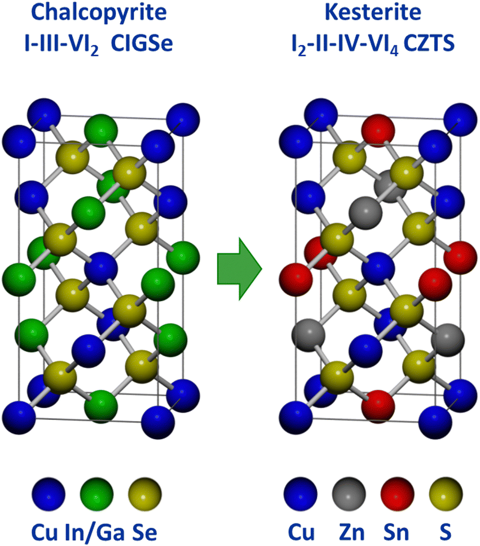 | ||
| Fig. 8 Comparison of chalcopyrite and kesterite crystal structures.93 | ||
In 2009, three groups independently published the synthesis of multinary Cu2ZnSnS4 nanoparticles.95–97 Building off of Cu(In,Ga)S2 nanoparticle work, the Purdue team produced 7.2% efficient Cu2ZnSn(S,Se)4 devices by coating and selenizing Cu2ZnSnS4 nanoparticles.98 Further optimization of this process lead to an efficiency boosts up to 9.0%.99 The Agrawal group also showed that amine–thiol chemistry was applicable to this material system as well, reactively dissolving precursors like Zn, Sn, SnS, and SnSe.30 Zhang et al. showed that the amine–thiol chemistry could enable the molecular precursor approach for Cu2ZnSn(S,Se)4 and produced devices achieving an efficiency of 7.86%.100
Similar to their work on Cu(In,Ga)(S,Se)2, the Hillhouse group developed DMSO-thiourea chemistry for applications in Cu2ZnSn(S,Se)4.101 The benign nature of this chemistry combined with the non-toxic nature of Cu2ZnSn(S,Se)4 makes this route particularly attractive for industrial applications. By addressing defects related to the oxidation state of the Sn precursors (Sn2+vs. Sn4+), the Xin group used this same type of chemistry to produce solar cells with efficiencies up to 12.4%.102
Hydrazine–chalcogen chemistry has also been highly successful in Cu2ZnSn(S,Se)4 research. In particular, the Mitzi group at IBM used this chemistry to produce a series of high efficiency devices.103–105 While molecular complexes can be obtained for the tin precursor through reactions of SnSe with Se in hydrazine, a nanoparticulate ZnSe(N2H4) is generated when Zn metal is added to the precursor ink.103 To improve the ink quality, the Mitzi group switched to a zinc salt for a fully molecular precursor ink.106 Ultimately, optimization of this new ink lead to a record device efficiency of 12.6%.107
While there are many example of Cu(In,Ga)(S,Se)2 research influencing Cu2ZnSn(S,Se)4 processing, influence in the reverse direction has also occurred. A major example of this is in regard to a selenium liquid flux for converting nanocrystalline sulfide precursor films into large-grain selenide absorber layers. The sulfide precursor route first used in Cu(In,Ga)(S,Se)2 work was quickly adopted for Cu2ZnSn(S,Se)4 solar cells.60,95 However, the presence of a selenium flux that enables both grain growth and conversion to a selenide material was first identified by Hages et al. for Cu2ZnSn(S,Se)4.77 This work was then highly influential on the selenium flux mechanism for Cu(In,Ga)(S,Se)2 proposed by McLeod et al.78
Unfortunately, after the record efficiency of 12.6% was obtained in 2014, no further progress in efficiency was made for many years.107 Researchers began to dive deeper into the defect chemistry, particularly in comparison to Cu(In,Ga)(S,Se)2, to see if there are fundamental features of this material that will limit its ability to obtain high efficiencies above 20%. Because of the more complicated quaternary crystal structure, a large number of antisite defects and defect clusters are possible. Researchers predicted that high concentrations of these defects will likely exist in the material, including some deep level defects.108–110 The Agrawal group contributed to the literature of defect chemistry of kesterite absorber layers through a number of optoelectronic characterization studies.111–115 Part of the reason that antisite defects can so readily form in this material is the similarity in size of the Cu+, Zn2+, and Sn4+ cations (Fig. 9).116,117 To try and limit these defects, a large amount of research has gone into partial or complete substitution of the cations in Cu2ZnSn(S,Se)4 with cations of different sizes. This strategy has aided in recent record efficiencies in substituted Cu2ZnSn(S,Se)4 and offers a new path for this material to obtain higher efficiencies.
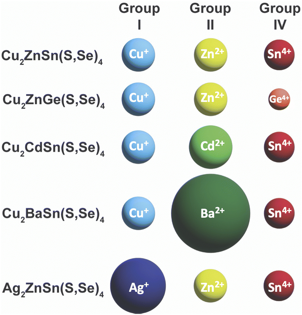 | ||
| Fig. 9 Comparison of ionic radii of cations in Cu2ZnSn(S,Se)4 and substituted variants. Ionic radii are based on a coordination number of 4, except for Ba2+ with a coordination number of 8: Cu+ – 0.6 Å, Ag+ – 1 Å, Zn2+ – 0.6 Å, Cd2+ – 0.78 Å, Ba2+ – 1.42 Å, Sn4+ – 0.55 Å, Ge4+ – 0.39 Å.117 | ||
Cu2ZnSn(S,Se)4-inspired materials
The immense initial success Cu2ZnSn(S,Se)4 followed by stagnation in device efficiency lead to extensive investigation into related materials that might overcome the intrinsic defect limitations in Cu2ZnSn(S,Se)4. These strategies ranged from partial substitution of one or more elements to complete replacement of one or more of the elements in Cu2ZnSn(S,Se)4. In particular, changing the compositions to increase the size difference between the cations is a prevalent strategy to decrease the concentration of antisite defects. A variety of monovalent, divalent, and tetravalent cations can be considered (Fig. 9). The most successful substitutions have been Ag+ for Cu+, Cd2+ or Ba2+ for Zn2+, and Ge4+ for Sn4+. However, determining improvements to the optoelectronic properties is not always straightforward. As the substitution not only affects defect formation energies, but also band alignment, it is possible to improve the absorber material but get worse device efficiencies because the device architecture is no longer appropriate for new absorber. Therefore, a variety of approaches at the material and device level are needed for a wholistic analysis. A detailed comparison of optoelectronic properties and device performance from alloyed-kesterites and kesterite-inspired materials was recently given in a review article by Hadke et al.118The Agrawal and Hillhouse collaboration led to the first exploration of Ge-substitution in solution processed Cu2Zn(Sn,Ge)(S,Se)4 solar cells. Ford et al. were able to make alloyed Cu2Zn(Sn,Ge)S4 nanoparticles with bandgap tuning using various Ge/Sn ratios with GeCl4 as the Ge-source.119 Coating and selenizing these nanoparticles enabled device efficiencies up to 6.8% at a Ge/(Ge + Sn) ratio of 0.7.119 Subsequently, at a much lower Ge/(Ge + Sn) ratio of 0.17, the device performance was increased to 8.4%.120 Hages et al. tuned the bandgap of Cu2Zn(Sn,Ge)(S,Se)4 by controlling the Ge content in Cu2Zn(Sn,Ge)S4 nanoparticles and carefully accounting for Ge loss during the high temperature selenization treatment.121 For a Ge/(Ge + Sn) atomic ratio of 0.3, total area efficiencies of up to 9.4% and increased minority charge carrier lifetimes were achieved. Hages et al. have conducted comparative analyses of Ge substituted and non-substituted Cu2ZnSn(S,Se)4 solar cells and concluded that Ge substitution may partially (but not fully) address defects in this material class.111,121–123 Vacuum deposited Cu2Zn(Sn,Ge)(S,Se)4 devices have surpassed the efficiencies of solution processed devices at 11.8% and 12.3% in different reports, but have yet to exceed record efficiencies of Ge-free Cu2ZnSn(S,Se)4.124,125
Cd-alloying and substitution for Zn is another popular strategy. Because of the similar chemistry between Cd and Zn, many of the same solution-based methods can often be used. For example, cadmium acetate can be substituted for zinc acetate with thiourea in 2-methoxyethanol.126 The substitution of Cd for Zn may reduce deep-level defects and minimize bandgap fluctuation in the material, but also leads to a crystal structure transformation from kesterite to stannite at higher Cd content.126,127 Record Cu2(Zn,Cd)Sn(S,Se)4 devices were produced by spin coating inks made with thiourea and 2-methoxyethanol chemistry, and achieved a notable efficiency of 12.6% at a Cd/(Cd + Zn) ratio of 0.4.128 However, this substitution on its own has yet to surpass the efficiencies of Cd-free Cu2ZnSn(S,Se)4 and the toxicity of Cd is concerning.
Ba-alloying and substitution for Zn has also been investigated due to the much larger ionic radius of Ba2+ compared to Zn2+. Unlike Ag, Ge, and Cd, Ba has a very different chemical nature compared to the base elements in Cu2ZnSn(S,Se)4. In particular, it is highly oxophylic and barium sulfate secondary phases are highly thermodynamically stable.129,130 Therefore, extra care has to be taken to solution-process Ba-containing metal chalcogenides. For example, this generally includes chemical storage and handling in an inert atmosphere (Schlenk line or glovebox) and using anhydrous solvents.131 The Mitzi group at Duke University has studied solution processed deposition of Cu2BaSn(S,Se)4 films using thiourea-DMSO chemistry and noted the challenge with obtaining barium sulfate secondary phases.132 In replacing Zn2+ with Ba2+ there is also a significant shift in crystal structure, with the +2 cation changing from 4-fold to 8-fold coordination. On the other hand the Cu and Sn maintain a similar network as part of corner sharing tetrahedra.133 Promising efficiencies of up to 6.5% have been achieved from solution processed Cu2BaSn(S,Se)4 solar cells but deep defects may limit this material moving forward.134,135
Ag-alloying in Cu2ZnSn(S,Se)4 is a particularly interesting option that has shown arguably the most promise to date.136 Many of the same chemistries used for copper chalcogenides can be extended to silver chalcogenides, though with the added challenge that many silver compounds can be sensitive to light.32,46,137 From the Agrawal group in 2016, Hages et al. introduced alloyed (Ag,Cu)2ZnSn(S,Se)4 thin films made by the solution deposition of (Ag,Cu)2ZnSnS4 nanoparticles.138 The addition of silver alloying improved the film morphology and lengthened carrier lifetimes. At a Ag/(Ag + Cu) ratio of 0.05, a device efficiency of 7.2% was achieved. Hu et al. went a step further showed that the fully substituted Ag2ZnSnS4 nanoparticles could also be synthesized.139 The fully substituted form of Ag2ZnSnSe4 may have the best defect properties of any of the kesterite-inspired materials.136 However, high levels of silver content in (Ag,Cu)2ZnSn(S,Se)4 has been shown to worsen device efficiency when using the conventional architecture employed by Cu(In,Ga)(S,Se)2 and Cu2ZnSn(S,Se)4 solar cells. This may be in part due to shifting of band positions in the material, but importantly the materials also reduces its hole concentration with increased Ag-alloying, becoming intrinsic and then weakly n-type with full Ag-substitution.140 As the Cu(In,Ga)(S,Se)2 device architecture was designed for a p-type absorber material, the poor performance with Ag2ZnSnSe4 is expected. With a redesigned device architecture that was still limited to a simulated efficiency to 6.4%, Gershon et al. used vacuum deposition to produce 5.18% efficient Ag2ZnSnSe4 solar cells.141,142 Recently, by using a new alkahest dissolution of Ag, Zn, and Sn, Turnley et al. were able to solution deposit pure Ag2ZnSnSe4 thin films by dropcasting.35 These are promising results and should prompt further investigation in designing a better absorber layer and device architecture for Ag2ZnSnSe4 solar cells.
Recently, a new certified record efficiency of 13.8% (total area) for an alloyed Cu2ZnSn(S,Se)4 solar cell has been achieved.143 Zhou et al. solution processed a (Ag,Cu)2ZnSn(S,Se)4 absorber layer with a Ag/(Ag + Cu) ration of 0.1 using thiourea and 2-methoxyethanol inks. Impressively, the ink formulation and coating was done in air, which could enable an easier transition to industry.143 While the long-time stagnation in efficiency may have diminished some enthusiasm about Cu2ZnSn(S,Se)4 PV, new strategies in alloyed (Ag,Cu)2ZnSn(S,Se)4 and recent efficiencies gain offer renewed hope that this class of materials can enable high efficiency and solution processable solar cells from non-toxic elements.
Copper pnictogen sulfides
Another class of metal chalcogenide semiconductors containing exclusively earth-abundant elements is the copper pnictogen sulfides. Of the pnictogens, phosphorus is particularly earth abundant. And while arsenic and especially antimony are not as abundant, they are produced in large volumes and tend to be reasonably cheap (though future production may be influenced by policy decisions).144 Various Cu–P–S, Cu–As–S, and Cu–Sb–S materials have been synthesized through solution processing and considered for optoelectronic applications. While much of the chemistry related to copper and sulfur can be extended from previous work on solution processed Cu(In,Ga)(S,Se)2 and Cu2ZnSn(S,Se)4, the pnictogens do introduce new challenges, particularly due to their multiple stable oxidation states.144Copper phosphorus sulfides would be extremely attractive from an earth-abundance standpoint and the Agrawal group has studied Cu3PS4 in particular. Sheets et al. developed a sequential colloidal nanoparticle synthesis whereby Cu nanoparticles are made and then reacted with P2S5 in trioctylphosphine to produce Cu3P. The Cu3P was then reacted with thiourea to generate Cu3PS4.145 Graeser and Agrawal tailored the CuCl2, P2S5, and 1-dodecanethiol system to report direct one pot synthesis of Cu3PS4 and Cu6PS5Cl nanoparticles.146 For PV applications, Cu3PS4 has a bandgap that is too large to serve as an absorber material (2.3–2.4 eV). However, its band positions allowed a Cu3PS4 nanoparticle layer to serve favorably as a hole selective layer for halide perovskite solar cells.147 Cu3PS4 has also been considered as an electrode in sodium-ion batteries.148
Copper arsenic sulfides have also been identified as interesting, earth-abundant candidates for semiconductor applications, though the use of arsenic raises concerns of toxicity.149 Notably, there are a number of different copper arsenic sulfide phases including enargite Cu3AsS4, luzonite Cu3AsS4, sinnerite Cu6As4S9, and tennantite Cu12As4S13.150,151 The Agrawal group first developed a colloidal nanoparticle synthesis for the luzonite and tennantite phases through the hot injection of CuCl, AsCl3, and sulfur in oleylamine, with crystal phase being controlled by reaction temperature.152 McClary et al. later used these luzonite Cu3AsS4 nanoparticles as colloidal precursors for solution deposited copper arsenic sulfide thin films.150 To prevent arsenic and sulfur loss during the grain growth step, the films were heat treated in a sealed ampule with As2S5, which could also enable an arsenic sulfide liquid flux. During this process, the luzonite nanoparticles converted to a coarse grain enargite film.150 The enargite phase of Cu3AsS4 has a near optimal bandgap of 1.4 eV for a single junction solar cell. However, despite reasonably high carrier lifetimes from enargite Cu3AsS4, the resulting solar cells had efficiencies below 1%.150,153,154 Recently, amine–thiol based molecular precursors were used to successfully alloy Ag into Cu3AsS4 up to Ag/(Ag + Cu) atomic ratios of 0.14, however solar energy conversion efficiencies remained below 1%.155
The first synthesis of Cu3SbS4 nanoparticles was reported by Van Embden and Tachibana in 2012 and was followed with the synthesis of CuSbS2, Cu3SbS3, and Cu12Sb4S13 nanoparticles.156–158 In 2016, Agrawal's group extended the methods of Cu3AsS4 nanoparticle synthesis to synthesize Cu3(Sb1−xAsx)S4 nanoparticle alloys to tune the optoelectronic properties for device applications.159,160 The bandgap was found to decrease from 1.2 eV to 0.84 eV as the value of x was decreased from 1 to 0 in the alloyed nanoparticles, indicating the potential for some of the alloyed compositions to be used as the bottom absorber in tandem solar cells. Much lower bandgap materials such as Cu3SbS4 are likely better suited for thermoelectric applications.161 Interestingly, by using amine–thiol chemistry to make sulfur-free selenium solutions, Balow et al. synthesized selenide Cu3(Sb1−xAsx)Se4 alloyed nanoparticles with values of x ranging from 0 to 1 and demonstrated the use of thin films derived from these nanoparticles for room-temperature thermoelectric devices.162 McClary et al. reported the synthesis of tetrahedrite–tennantite (Cu12Sb4S13–Cu12As4S13) nanoparticle alloys for the entire composition range of Sb to As.163
Chalcogenide perovskites
Chalcogenide perovskites have garnered interest for their enhanced stability compared to the halide perovskites while retaining bandgaps in the visible range.164,165 Like the halide perovskites they have an ABX3 compositions, but in this case A is commonly a +2 cation, B is commonly a +4 cation, and X is a −2 chalcogen anion. Their earth-abundant and non-toxic compositions are appealing. Additionally, they are predicted to have substantial defect tolerance, though experimental evidence of strong optoelectronic properties is still needed.166 The most studied chalcogenide perovskite is BaZrS3, but several others containing different combinations of alkaline earth or early transition metals are known.167–169 Generally, most observed and predicted chalcogenide perovskites have sulfide anions, but a selenide perovskite has been found as well.170While interest in chalcogenide perovskites has been growing, synthesis challenges limited the extent of research on these materials. Initially, methods like solid-state synthesis, sulfurization of oxide perovskites, and vacuum deposition were used to make chalcogenide perovskites. But these techniques often utilized temperatures around 1000 °C.167,168,171,172 This limits the ability of these synthesis methods to be used in device fabrication as most of the common substrates and conductive contact layers cannot tolerate these temperatures. As such, the Agrawal group and several other labs sought to develop low-to-moderate temperature synthesis techniques, especially via solution-based methods.
Several groups, including the Agrawal group, published low-to-moderate temperature syntheses of BaZrS3 in 2022. The Scragg group utilized physical vapor deposition to make thin films, and upon careful protection against oxide formation the sulfurization temperature could be dropped to around 600 °C.173,174 In noteworthy developments, both the Hages group and the Creutz group developed colloidal nanoparticle synthesis methods making use of reactive metal organic precursors.175,176
On the other hand, the Agrawal group focused on direct-to-film solution-based methods. This was first achieved by Turnley et al. utilizing a mixed ink containing both molecular and nanoparticle precursors.177 As a barium source a soluble barium thiolate was synthesized. For the zirconium source, nanoparticulate zirconium hydride was used. Upon coating and annealing, this produced films containing BaS and ZrH2 which could be sulfurized at temperatures of 550–575 °C to form BaZrS3. By switching the ZrH2 to HfH2 or TiH2 this method could also be extended to make the chalcogenide perovskite BaHfS3 or the hexagonal BaTiS3 (Fig. 10a).177 Vincent et al. subsequently showed that during the sulfurization process, a barium polysulfide (BaSx where x > 3) plays an important role as a liquid flux during the formation of the ternary chalcogenide perovskite (Fig. 10b).178 It should be noted that work from the Hages group corroborated the importance of a barium polysulfide liquid phase in the moderate temperature growth of Ba-containing chalcogenide perovskites.179 In collaboration with the Bart group, the Agrawal group also developed a fully molecular approach to synthesizing BaZrS3 and BaHfS3.180 Pradhan et al. utilized CS2 insertion chemistry to make barium dithiocarboxylates and zirconium or hafnium dithiocarbamates as soluble molecular precursors. After coating, a similar sulfurization process at temperatures around 575 °C enabled the formation of BaZrS3 and BaHfS3.180
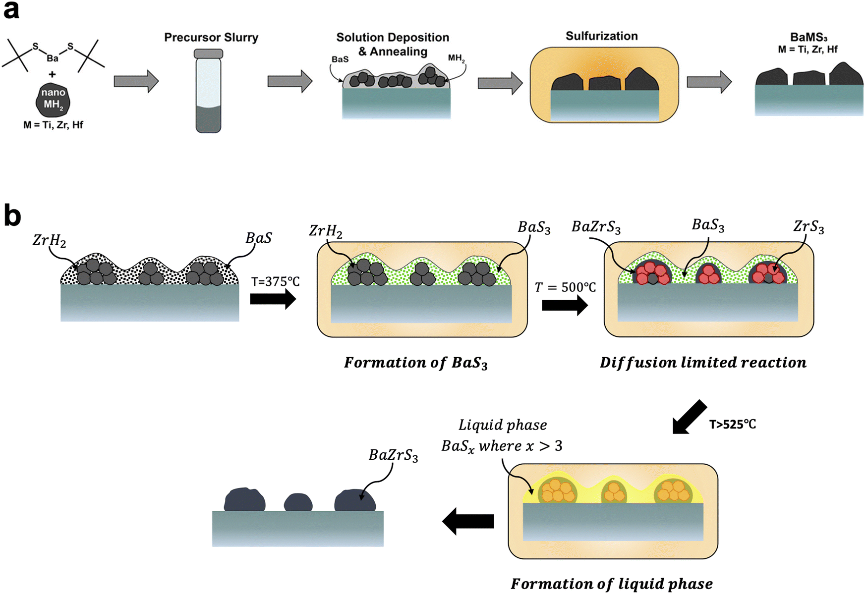 | ||
| Fig. 10 (a) Schematic of solution deposition approach for the synthesis of BaMS3 (M = Ti, Zr, Hf) materials. Reprinted with permission.177 Copyright 2022 American Chemical Society. (b) Schematic of the barium polysulfide liquid-flux assisted formation of BaZrS3. Adapted with permission.178 Copyright 2023 Wiley-VCH. | ||
Overall, solution processing of chalcogenide perovskites has been influenced by the work done on more traditional metal chalcogenide semiconductors but also has some notable differences. Similar to Cu(In,Ga)(S,Se)2 and Cu2ZnSn(S,Se)4, nanoparticle syntheses have utilized oleylamine as the high-boiling point solvent and ligand. Additionally, molecular precursors have included metal thiolates and other metal organics that contain metal–sulfur bonding. However, the metals in chalcogenide perovskites are notably different than those in traditional metal chalcogenide semiconductors. In Cu(In,Ga)(S,Se)2, Cu2ZnSn(S,Se)4, and CdTe, late-transition and post-transition metals constitute the cations. But the chalcogenide perovskites use alkaline earth and early-transition metals. This means that the cations in chalcogenide perovskites tend to be quite hard and oxophilic, creating a mismatch with the softer chalcogenide anions. The challenges in working with this type of metal chalcogenide was recently covered by Zilevu and Creutz.181 Looking across the chalcogenide perovskite literature, it is clear that synthesis methods need to be designed carefully. Methods that have worked for other metal chalcogenide may not be sufficient to produce chalcogenide perovskites. For example, the Agrawal group has typically used solvents as-received in Cu(In,Ga)(S,Se)2 research. But trace water impurities in these solvents inhibit chalcogenide perovskite formation and contribute to highly stable metal oxide or sulfate secondary phases. Therefore, extensive solvent drying techniques are standard in solution processed chalcogenide perovskite synthesis.
On the other hand, metal oxides would be cheap and easy-to-handle precursors if they could be converted to the chalcogenide perovskites at reasonable temperatures. Historically, sulfurization of oxide perovskites was done at extremely high temperatures. However, the Agrawal group has recently shown that the thermodynamics around the sulfurization step can be altered by heating in the presence of both HfH2 and sulfur.182 The sulfur initially reacts with the HfH2 to produce HfS3 and H2S. This HfS3 then functions as a powerful oxygen trap through the formation of HfO2 and the oxygen can be transported out of the oxide perovskite to the trap through an H2O/H2S shuttle. While a simple sulfurization is not able to convert a BaZrO3 film into BaZrS3, this reconfigured sulfurization changes the thermodynamics to facilitate the conversion at 575 °C. This process then enables the use of solution processed oxide perovskites as precursors for chalcogenide perovskite thin films with moderate temperature processing.182
While the differences in chalcogenide perovskite chemistry create some challenges in their synthesis, there are also new opportunities. For example, these alkaline earth and early transition metal chalcogenides have much more ionic bonding character than Cu(In,Ga)(S,Se)2, which can lead to different and interesting properties. These opportunities for chalcogenide perovskites and related materials are discussed further in the next section.
Opportunities for future development
Significant progress has been made in the solution processing of metal chalcogenide semiconductors for thin film PV applications, with solution processed Cu(In,Ga)(S,Se)2 devices achieving efficiencies above 18% and the state-of-the-art in (Ag,Cu)2ZnSn(S,Se)4 utilizing solution deposition.73,143 However, there are still a number of opportunities for further development, both from a fundamental science standpoint and in the pursuit of achieving a commercial impact.Amine–thiol alkahest chemistry
Fig. 11 sums up various insights and methods that have been studied and developed by several groups over the past decade to tailor amine–thiol solution chemistry to synthesize various inorganic chalcogenide nanoparticles and thin films. Due to the versatility and promise of this chemistry, it will now be discussed in detail.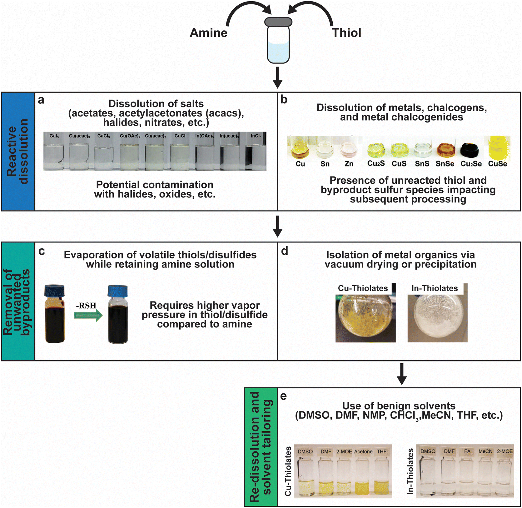 | ||
| Fig. 11 Versatility of amine–thiol solutions to tailor molecular precursor inks for a variety of nanoparticle and thin film applications. (a) The ability of amine–thiol solution to dissolve metal salts. Reprinted with permission.36 Copyright 2016 Royal Society of Chemistry. (b) The ability of amine–thiol solutions to dissolve metals, chalcogens, and metal chalcogenides. Reprinted with permission.30 Copyright 2016 Royal Society of Chemistry. (c) The ability to remove volatile biproducts from the ink. Reprinted with permission.188 Copyright 2014 Royal Society of Chemistry. (d) The ability to completely isolate metal thiolates and (e) the ability of redissolve metal thiolates for ink tailoring. Reprinted with permission.28 Copyright 2019 American Chemical Society. | ||
A mixture of monoamine (RNH2) or diamine (NH2RNH2) with a monothiol (RSH) or a dithiol (HSRSH) provides a potent mixture that is capable of reactively dissolving a large array of precursors. This includes traditional metal salt precursors like nitrates, halides, acetates, and acetylacetonates (Fig. 11a). However, oxygen and halogens present in the salts may not leave from the amine–thiol solutions and can get incorporated in the final nanoparticles or films. Murria et al. observed that the dissolution of CuCl2 and CuCl in 1-propanethiol and n-butylamine resulted in copper thiolate chlorides and alkylammonium chlorides in addition to the desired copper thiolates.33 Thin films prepared from these solutions revealed persistent chlorine impurities. It was also found that adding a chalcogen (S or Se) to the solutions and annealing at high temperatures helps in volatilizing the impurities.33,100 Another challenge while using chloride precursors while preparing Cu(In,Ga)(S,Se)2 precursor films was observed by Zhao et al.36 They observed that the use of inks containing Cl− ions results in the loss of Ga3+ as GaCl3 at lower annealing temperatures prior to its incorporation into Cu(In,Ga)(S,Se)2. When using Bi2O3 as a precursor in a solution of ethylenediamine with either ethanethiol or ethanedithiol, Brutchey's group observed Bi2O3 in the deposited sulfide material.183
In order to avoid halide, oxide, or sulfate secondary phases in the nanoparticles and the thin films due to the use of metal salt precursors, the use of precursors that avoid such anionic impurities is desirable.33,132,184,185 Herein lies the benefit of the “alkahest” chemistry of amine–thiol reactive solvent systems.186,187 Using the reactive solvent systems can enable the dissolution of precursors that are generally insoluble, such as metals, metal chalcogenides, and chalcogens at or near room temperatures (Fig. 11b).26,30,186,188 It should be mentioned that such solubilities could depend on the choice of amine–thiol pair. For example, Agrawal's group has reported solubility of Se in monoamine–monothiol188 and of metal chalcogenides (e.g. Cu2S, Cu2Se, CuS, CuSe, SnS, SnSe, In2S3, In2Se3, Ag2S and Ag2Se) and metals (e.g. Cu, Zn, Sn, and In) in an monoamine–dithiol,29,30 whereas Brutchey's group reported use of diamine–dithiol mixtures to dissolve V2VI3 chalcogenides.186 Similarly, it is known that while Se and S dissolve in almost any amine–thiol pair, Te does not dissolve in an monoamine and thiol mixture but it is found to dissolve in a diamine and ethanethiol mixture.189,190 Currently, a fundamental understanding of the impact of the choice of an amine–thiol pair on the solubility of a metal or its chalcogenide is not available. Experimental observation has resulted in a breadth of knowledge of useful precursor–solvent combinations, but a deeper theory that provides a predictive ability would allow for a major step forward in this alkahest chemistry.
Another aspect of the amine–thiol chemistry that is less understood is the nature of the metal compounds that are formed upon dissolution in an amine–thiol solvent and their reaction chemistry during subsequent processing for nanoparticle and thin film formation. Such an understanding is essential for tailoring the solution chemistry to obtained desired materials properties. A few studies have begun to shed some light on these aspects. In an early study, Vineyard reported formation of alkyl polysulfides when sulfur is added in a mixture of monothiol in either methanol or methylene chloride with n-butylamine in an amount of 2 to 2.5% of the thiol.191 On the other hand, there may be a need to revisit this sulfur dissolution chemistry as the amine–thiol alkahest chemistry described here generally uses much higher amine to thiol ratio in the range of 0.1 to 10. Upon dissolution of Se in a monoamine (R1NH2) and ethanethiol, Agrawal's group did not see alkyl polyselenides, but polyselenide anions (Sex2−) with various chain lengths counterbalanced by R1NH3+ cations (Fig. 12).188,190 In an alkylammonium polyselenide molecule, electrons that reduce the Se to form Sex2− result from the combination of two thiolate anions (RS−) to form a neutral diethyl disulfide molecule. Quantitative NMR revealed that increasing ratio of thiol/Se led to decrease in average chain length, x, of Sex2− ions from slightly above 6 to below 4. Interestingly, no Se–S bond was observed in the solution. However, replacement of the monoamine with a diamine (ethylenediamine) led to Sex2− anions at lower thiol/Se ratios and formed thiol-coordinated polyselenide ions (RSSey−) and eventually RSSe− anions with no Se–Se interaction in the solution with increasing thiol/Se ratio. The dissolution of Te in ethylenediamine and ethanethiol always indicated thiol-coordinated polytellurides. The difference between the two amine solutions could be due to different interactions in diammonium cation solutions vs. monoammonium cation solutions or due to chelating nature of ethylenediamine resulting in a possible intermediate pathway for Se–ethylenediamine coordination.190 Interestingly, while Te is not soluble in a monoamine–monothiol mixture, it was found to co-dissolve with Se revealing SexTey2− ions exclusively without any interaction of Se or Te containing species with the thiol's S.190 It is suggested that the Sex2− ion formed in this solution may act as a nucleophile similar to the RS− ion, leading to the dissolution of Te through the formation of SexTey2− complexes.190 This phenomenon could also explain the dissolution of some of the other metals when co-dissolved with Se but which remain nearly insoluble in the absence of Se.189 The Agrawal group used the co-dissolution of Se and Te in butylamine and ethanethiol to prepare uniformly alloyed PbSenTe1−n nanoparticles.190
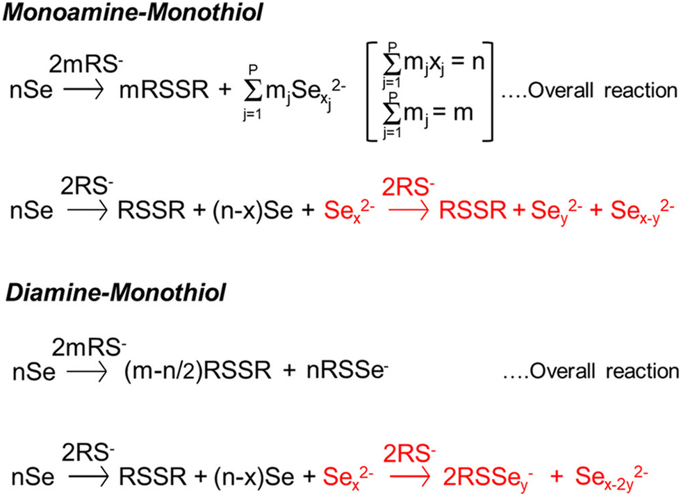 | ||
| Fig. 12 Reaction schemes for the reactive dissolution of selenium in different amine–thiol solutions. Reprinted with permission.190 Copyright 2020 American Chemical Society. | ||
A few studies on the formation of thiolatometallate ions upon the dissolution of metals in the amine–thiol solutions have also been done. Fig. 2a shows the formation of an In-thiolate molecule which takes place with the simultaneous liberation of hydrogen. Similar linear and compact cluster structures for Cu complexes have been identified.28,33 Upon heating, these metal thiolates can decompose into metal sulfides (Fig. 2b). More studies characterizing thiolatometallate and thiolatoselenometallate species in these solutions are needed. An example of the importance of connecting metal thiolate chemistry to the synthesis of metal chalcogenides is the work of the Tao group.192 Careful control of the thiolate structure has enabled them to use copper thiolate liquid crystals as a template to synthesize copper sulfides with anisotropic shapes.
After dissolution of metals, metal chalcogenides, and chalcogens, the amine–thiol mixture contains a number of sulfur-containing species including unreacted thiol, metal thiolates, and byproducts such as disulfides. This has several consequences when this solution is used for subsequent processing to prepare nanoparticles and thin films. First, it is difficult to prepare sulfur free chalcogenides from these solutions. Second, the presence of multiple sulfur species could influence the properties and the homogeneity of the final chalcogenide material that is formed. Third, thiols are malodorous and the resulting solution requires careful handling to alleviate safety concerns. Fourth, the ability to tailor the properties of the solution via solvent engineering is limited. As shown in Fig. 11c–e, the Agrawal group has been working to address these challenges.
A quick note on using thiols in a research lab is merited. Given the toxic and malodorous nature of thiols, the use of thiols in the Agrawal group is restricted to fume hoods and gloveboxes. Thiol-containing waste is stored in ventilated waste cabinets and respirators are available in case of emergency.
When a solution of Se in amine–thiol is directly used for the synthesis of nanoparticles and films, some incorporation of sulfur is often observed in the resulting material due to the presence of active thiol and disulfide compunds.34,188,193,194 The first solution to overcome this challenge was suggested through the dissolution of Se in an heavy amine and more volatile thiol followed by low temperature evaporation of all the sulfur containing species while keeping the formed polyselenides dissolved in the heavier amine (Fig. 11c).188,195 It should be noted that if the reverse is adopted, whereby a lighter amine is used and selectively evaporated while retaining heavier thiol, Se was found to precipitate out of the solution. Thus, Se was dissolved in an ethanethiol–oleylamine mixture at room temperature, and residual ethanethiol and byproduct diethyl disulfide were removed under vacuum reflux at ∼120 °C. The resulting Se precursor in oleylamine was used to synthesize sulfur-free nanoparticles of Se, PbSe, CuInSe2, Cu2ZnSnSe2, cuprous selenide, and Cu3(As,Sb)Se4.162,188 While this is a useful method to obtain a sulfur-free selenium precursor, the method necessitates the use of heavier amine and is therefore more applicable to nanoparticle synthesis than direct thin film deposition.
The method in Fig. 11d stems from the observation that polyselenide and polytelluride species as well as most thiolatometallate/thiolatoselenometallate species in amine thiol solutions have low vapor pressures. This provides an opportunity for the judicious choice of volatile amines and thiols that can be evaporated following the dissolution using vacuum at low temperatures, leaving behind the intact metal and chalcogen complexes. These complexes were found to be generally soluble in a host of benign solvents often used in solution processing (Fig. 11e).28 One known exception is the dissolution of Te in a diamine and thiol mixture, whereby, evaporation of the liquids leads to the precipitation of phase pure Te making this route infeasible.189,190 Thus, Agrawal's team first dissolved Cu, In and Se powders individually in the mixtures of hexylamine and ethanedithiol at room temperature.28 Then for each Cu, In and Se solution, the entire liquid phase was evaporated under vacuum below 120 mTorr by stagewise heating starting at room temperature and then slowly increasing temperature up to approximately 60 °C, 70 °C, and 42 °C respectively. Each of the complexes, due to the use of low temperature evaporation, were found to be intact during this heat up process and were soluble in an array of solvents including dimethyl sulfoxide, dimethylformamide, formamide, acetonitrile, tetrahydrofuran, and 2-methoxyethanol.
There are multiple ramifications to the isolation of metal and chalcogen complexes and their redissolution in benign solvents. First, this enables the downstream use of these complexes in a more environmentally friendly and safe manner. In addition, competing reactions due to the presence of thiols and disulfides are eliminated. The use of dialkyl disulfides and monothiols as sulfur sources have resulted in the formation of wurtzite CuInS2 and Cu2ZnSnS4 nanoparticles, whereas the use of sulfur leads to the corresponding chalcopyrite phase.189,194,196,197 The observation of both chalcopyrite and wurtzite phases of CuInS2 nanoparticles synthesized from the monoamine and dithiol solutions containing Cu and In under different reaction conditions could be partially assigned to the relative reaction rates of different sulfur-containing species, especially thiol and dialkyl disulfides.32 Finally, the evaporation of solvents and by products provides the opportunity for solvent engineering. For example, during the deposition of Se–Te alloy film from an ethylenediamine–ethanethiol ink containing a Se and Te mixture, it was found that during the coating of subsequent layers, the coating ink would redissolve the previously deposited Se–Te layers which hindered the growth of thicker layers.198 This challenge was overcome by evaporating all the liquids from the ink at room temperature and redissolving the residue in pure ethylenediamine. Note that after evaporation of the liquids in presence of Se, Te does not precipitate out as phase pure Te and remains part of the complex which is readily soluble in the diamine.190 The modified diamine ink without a thiol does not dissolve metallic Se and Te during the coating of the subsequent layers and results in films of the desired thickness. Further solvent engineering was used by redissolving the isolated complexes in a 50–50 mixture of the diamine and another solvent such as dimethyl sulfoxide, dimethylformamide, and ethanolamine to further tailor and optimize the Se–Te alloy film morphology for solar cell performance.
Another method to remove unreacted thiols and disulfides from the dissolved precursor solutions has been used recently by the Agrawal group.35,79 In this precipitation–redissolution method, the dissolved precursor is precipitated by adding an antisolvent mixture, centrifuged, decantated, and redissolved in a suitable solvent (Fig. 13). The redissolved complex can be again reprecipitated and the cycle repeated for further washings. When feasible, the advantage of this method is that the complex can generally be isolated at room temperature without any need for heat and evaporation. As discussed below, the precipitation–redissolution method has further provided unanticipated opportunities using a selenium-based alkahest.
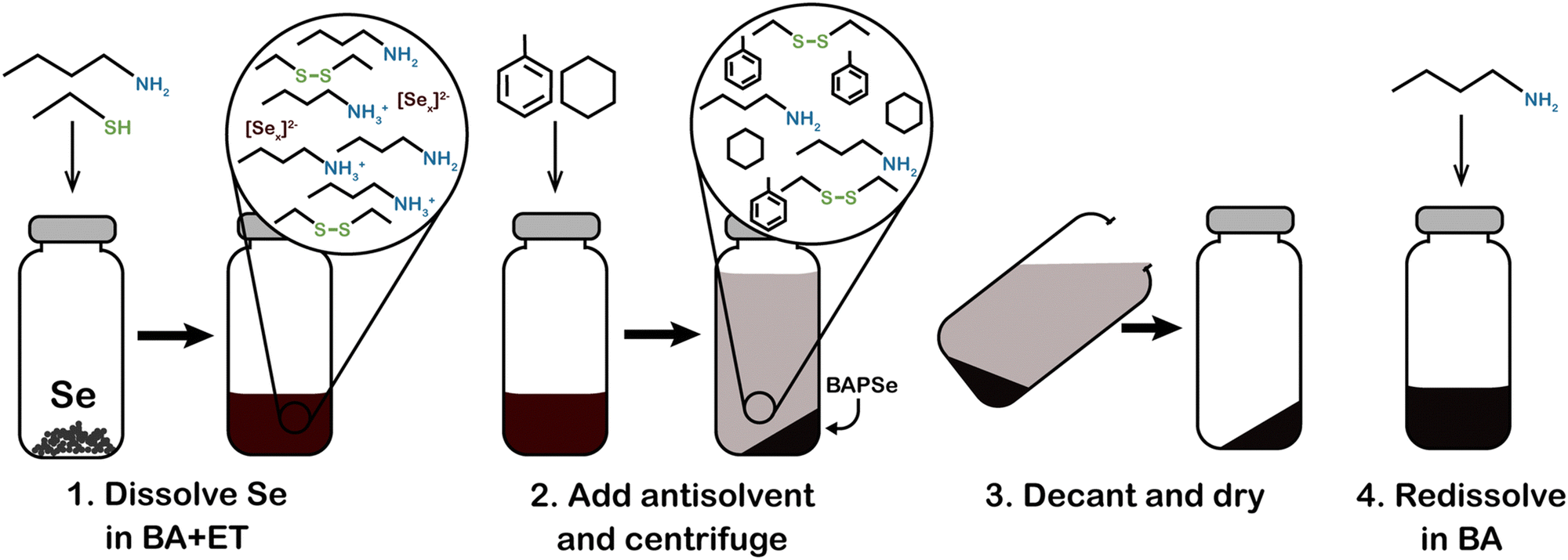 | ||
| Fig. 13 Schematic for a precipitation-based procedure for isolating alkylammonium polyselenides from a solution of butylamine (BA) and ethanethiol (ET). This same procedure can also be applied to isolating metal organics from amine–thiol solutions. Reprinted with permission.35 Copyright 2023 Royal Society of Chemistry. | ||
In this amine–thiol alkahest chemistry, metal precursors are dissolved in amine–thiol solutions as metal thiolates and are useful for making sulfide films. However, a recent observation by Turnley et al. provides an interesting possibility to make sulfur-free selenides for at least some of the metals using this chemistry.79 For example, it was found that when In or In2Se3 and Se are co-dissolved in butylamine and ethanedithiol solution with a Se to In ratio of 3 or greater, the complex formed in the solution does have In–S bonds. However, when the complex is precipitated using toluene–hexane (10:1 volume basis) and redissolved in butylamine (and further purified by subsequent redissolution and isolation steps) the In-containing complexes are changed into sulfur-free and soluble [InSex]− species. The absence of In–S bonds after precipitation–redissolution is indicative of the fact that chemical transformations do take place during these steps and could be used beneficially for certain applications. However, such complete removal of sulfur may not be observed with all metal precursors. For example, the use of the same precipitation–redissolution method with Cu2Se + 3Se, resulted in S/Cu atomic ratio of 0.40 and Se/Cu ratio of 1.4 and the method was unsuccessful in providing a completely S-free Cu complex. Potential processing benefits may result when the S-free or the S-poor and Se-rich complexes are used for selenide film preparations. For example, it is known that the use of sulfide thin films followed by selenization limits grain growth resulting in coarsened films of ∼1 μm with a bottom carbon containing fine grain layer for the remaining thickness of the film (Fig. 7a).79 The use of a Cu–In–Se ink, prepared by the precipitation–dissolution method, resulted in an annealed selenide precursor film with dramatically reduced carbonaceous peaks in the Raman spectra and without any evidence of sulfur in the material. Selenization of this film at 540 °C resulted in a coarsened absorber film of 2 μm or greater which is desirable for Cu(In,Ga)Se2 solar cells (Fig. 7b).
Another comment regarding the versality of the amine–thiol dissolution chemistry results from the impact of varying the C–C chain length within the alkyl groups of the amine and thiol molecules. In general, it is observed that the solubility of a given metal precursor decreases with the increase in the chain length within an amine and/or a thiol molecule. It also impacts the chemistry during subsequent processing steps. For example, Miskin et al. used various thiols with carbon chain lengths varying from 2 (ethanethiol) up to 12 (dodecanethiol) with butylamine to obtain PbX (X = S, Se, Te) nanoparticles and their assemblies (Fig. 14).199 The room temperature reaction between the Pb–amine–thiol precursor solutions prepared by dissolving PbI2 and the corresponding amine–thiol solution of chalcogens was found to be quite rapid resulting in immediate formation of particles upon mixing of the two solutions. Similarly, by greatly reducing the relative quantity of ethanethiol in the mixture with oleylamine (18 carbon chain length), individually dispersed 4 to 5 nm PbS and PbSe nanoparticles could be synthesized at room temperature.199 This example illustrates that along with carbon chain lengths in amine and thiol molecules, relative quantities of amine and thiol also influences rates of reaction, nucleation, growth, and shape of synthesized particles in subsequent processing.190,199,200
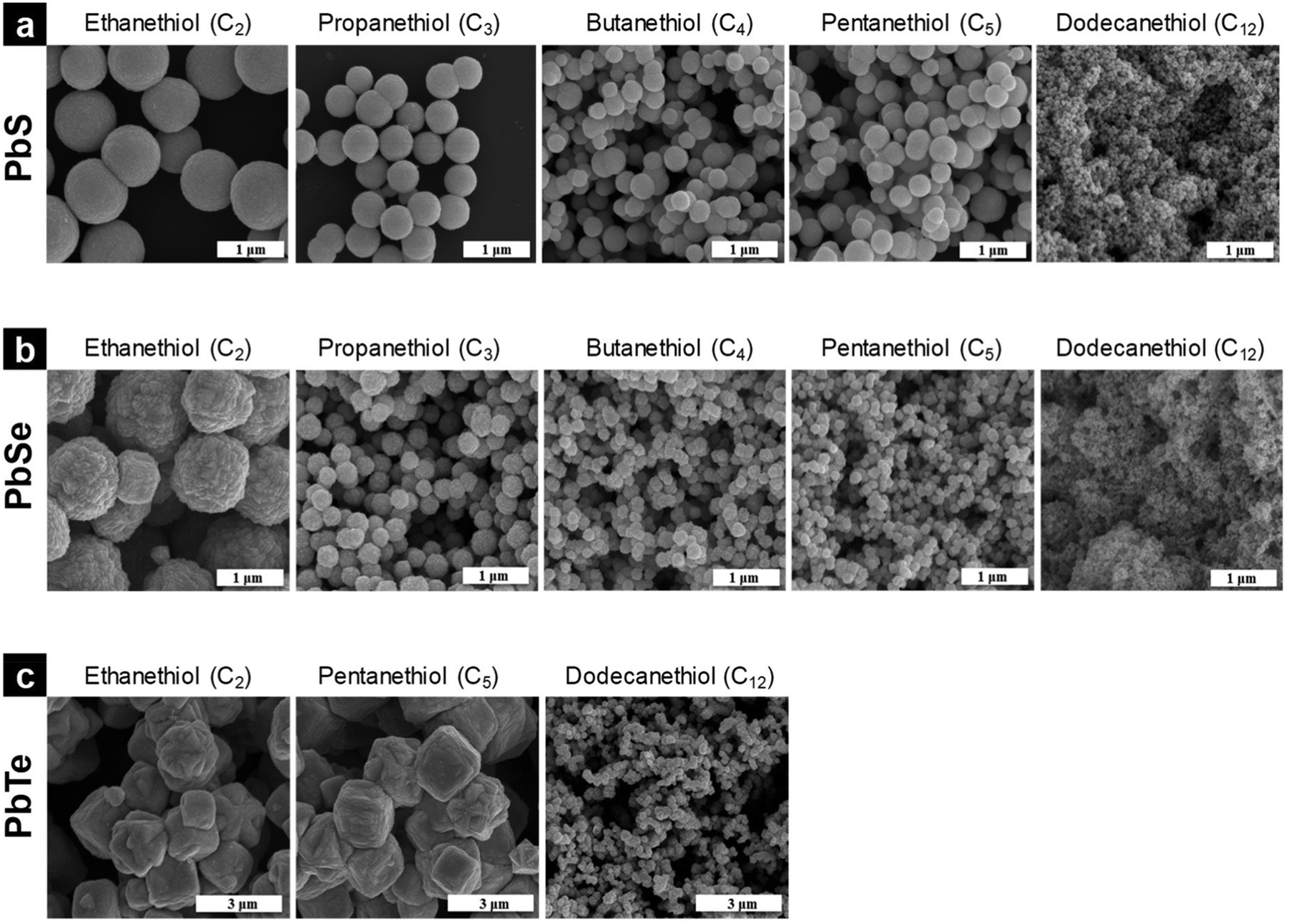 | ||
| Fig. 14 SEM images showing the morphological control via thiol selection in the synthesis of (a) PbS, (b) PbSe, and (c) PbTe particles. Reprinted with permission.199 Copyright 2019 American Chemical Society. | ||
Besides the synthesis of chalcogenide nanoparticles and thin films, precursor amine–thiol solutions can also be employed for ion exchange with chalcogenide materials. Micron-sized PbTe particles synthesized by the amine–thiol chemistry described above, were dipped in 0.5 M Se–ethylenediamine–ethanethiol solutions at room temperature for different durations.200 Within a few hours, the particles formed a core–shell structure with a Se-rich core and a Te-rich shell. The Te in the particle core was replaced with Se and all the particles showed the same level of Se exchange while retaining their uniform spherical shape and size. It should be noted that an attempt to directly prepare Se–Te alloyed particles from Se–Te and PbI2 inks in amine–thiols resulted in nonuniform size particles. While the initial rate of anion exchange is fast, it does saturate and ∼20% Te remained in the particles after a long exposure of seven days. It is well known that the extent of ion exchange, in addition to the differences between the lattice enthalpies of the starting and final materials, is also dependent on the entropy of exchange and the solvation/desolvation ion energies in the solvents used.201,202 As a result, even though on the basis of lattice enthalpy anion exchange of PbSe with Te is unfavorable, ∼45% of the Se could be exchanged from micron sized PbSe particles by exposing them to Te–ethylenediamine–ethanethiol solution. Note that Se has a much higher solubility in amine–thiol solutions than Te and that could facilitate some anion exchange in this case. Similar results for Se substitution were observed when PbS particles were exposed to Se–butylamine–ethanethiol solution. Deshmukh et al. also demonstrated room temperature anion exchange of Pb with Ag by dipping PbTe micron sized particles in a solution of AgCl in an ethylenediamine–ethanethiol mixture.200 Up to 96% of the Pb could be exchanged with Ag. Surprisingly, the microstructure of the particles remained intact, despite a crystal structure transition from cubic PbTe to monoclinic Ag2Te. However, room temperature cation exchange using amine–thiol chemistry has its own limitations as attempts to exchange Pb with Na, Cd, Zn and Bi in PbTe failed, suggesting a need for exploration of higher temperature ion exchange.
A selenium-based alkahest chemistry
As an offshoot of the amine–thiol dissolution chemistry research, the Agrawal group recently presented n-alkylammonium polyselenide ((RNH3)2Sex) solutions as a versatile, selenium-based solvent system for the synthesis of an array of phase pure metal selenide semiconductors.35 This finding was the result of two important observations: first, that Te could be made soluble in butylamine–ethanethiol solution as SexTey2− complexes when Te is otherwise insoluble in monoamine–monothiol mixtures,190 and second, through the method of precipitation–redissolution shown in Fig. 13, sulfur-free alkylammonium polyselenides (AAPSe) could be easily synthesized, isolated, and redissolved in an array of polar organic solvents including amines, dimethyl sulfoxide, or dimethylformamide. Turnley et al. showed that these AAPSe solutions can reactively dissolve a range of metals (including Cu, Ag, Zn, Cd, In, Ga, Sn, Ge, and As), metal chalcogenides, metal oxides, and metal halides.35 The ratio of selenium to metal was found to be an important factor in determining the amount of metal that could be solubilized. The reactive dissolution of metals in AAPSe solutions did not accompany any evolution of hydrogen and therefore, the dissolution mechanism was different from the one for the corresponding amine–thiol mixtures. It was identified that the mechanism consisted of metal oxidation via the reduction of longer polyslenide chains into smaller chains. These metal polyselenides were then used as convenient solution-based precursors for the synthesis of pure metal selenide semiconductor films including Ag2Se, Cu2−xSe, ZnSe, CdSe, In2Se3, SnSe2, CuInSe2, Cu(In,Ga)Se2, Cu2ZnSnSe4, and especially Ag2ZnSnSe4 (which has been notoriously tricky to make pure-phase due to competition with binary secondary phases). The AAPSe precursor inks were also used for the synthesis of nanoparticles such as chalcopyrite CuInSe2 and green-fluorescent nanorods of indium selenide. In the literature, the term “alkahest” is primarily associated with the amine–thiol reactive solvent systems.186 However, this concept of powerful reactive dissolution chemistry can be extended to AAPSe chemistry. Like the amine–thiol alkahest chemistry, there are limitations to the AAPSe alkahest. Not all metals tested by Turnley et al. dissolved in AAPSe solutions (specifically, Pb Bi, and Sb), and Ga did not dissolve on its own but did co-dissolve with In.35 Additionally, while not often labeled as such, hydrazine–chalcogen is another alkahest system, and beneficially contains no carbon.35The prospect of a deeper molecular level understanding of alkahest chemistry will enable the discovery of even more reactive solvent systems. A scientific understanding of the organometallic complexes formed and their dissociation products would help in tailoring the synthesis of chalcogenide semiconductor nanoparticles and thin films. And having a wider toolbox of alkahests will enable engineering of a broad range of materials for different applications, including solution processed photovoltaics. In particular, selenols and tellurols have been used in the synthesis of metal chalcogenides and given their relationship to thiols, they are interesting candidates for new alkahest systems.203–205
Alkali, alkaline earth, and early transition metal chalcogenides
As discussed earlier in this article, much of the research on metal chalcogenide semiconductors has delt with late transition or post transition metals. These materials have a more covalent bonding nature which can lead to useful properties like lower bandgaps in the near-IR and visible range.However, certain combination of metal chalcogenides that contain alkali, alkaline earth, or early transition metals have emerged as candidate materials with increased ionic bonding nature compared to conventional semiconductors but still having bandgaps in the visible range.181,206 This constitutes an exciting new opportunity for emerging materials that may address limitations in existing semiconductors. On the other hand, this class of materials poses a challenge from a synthesis perspective due to the different chemical nature of the constituent metals.
The chalcogenide perovskites are a clear example of this class of metal chalcogenide semiconductor. As has been previously discussed, intriguing properties but difficulties in synthesis have defined much of the work on chalcogenide perovskites to date.206 But since 2022, progress has been made towards the solution processing of the materials by the Agrawal, Hages, and Creutz groups.175–180 Lessons learned from this research can enable future work on related materials and includes findings such as design of reactive precursors, careful purification and sample handling to prevent oxide secondary phases, and the use of liquid fluxing agents to bypass solid state diffusion. Notably, the overwhelming majority of solution processed chalcogenide perovskite work has focused on BaZrS3. While there has been some exploration into BaHfS3, extending solution-processed chemistry to deal with Ca, Sr, Sc, Y, and the lanthanide elements could lead to the solution processing of other chalcogenide perovskites.
Additionally, there are a variety of materials with the same or similar elemental constituents as the chalcogenide perovskites but that have different crystal structures, such as hexagonal or needle-like crystals.164 By changing the stoichiometry of an ABX3 chalcogenide perovskite, the class of Ruddleden–Popper (RP) perovskites with 2D crystal anisotropy can by formed with an An+1BnX3n+1 composition.207 Examples of known RP chalcogenide perovskites includes Ba2ZrS4 and Ba3Zr2S7.165 Further, it is reasonable to assume there are a variety of undiscovered chalcogenide RP phases that could also possess interesting properties.
When considering binary metal chalcogenides from early transition metals, a variety of 2D van der Waals materials exist. Notably, this includes the transition metal dichalcogenides (TMDCs). MoS2 is perhaps the most well-known, but other molybdenum- and tungsten-based TMDCs have been studied extensively as well.208 Shifting to the group IV metals reveals a variety of less studied 2D materials. Like the chalcogenide perovskites, solution-based synthetic methods have proven difficult but could enable wider utilization of these materials.181 This group of materials includes the TMDCs TiS2, TiSe2, ZrS2, ZrSe2, HfS2, and HfSe2.209 However, there is a second class of 2D materials from these elements called transition metal trichalcogenides (TMTCs) which includes ZrS3, ZrSe3, HfS3, and HfSe3.210 Given the widespread interest in 2D materials from both a fundamental and applied perspective, these TMDCs and TMTCs merit further study by applying and extending the methods and tools described here.
Energy storage is an attractive opportunity for expanding the scope of how solution deposition of metal chalcogenides can impact energy technologies. To do this requires further expansion of this chemistry to utilize alkali and alkaline earth metals, most notably Li, Na, K, Mg, and Ca. The metal sulfides containing these elements have been proposed as both cathode materials and solid-state electrolytes in battery applications, but bottom-up synthesis from solution methods is not yet common in this context.211–213
Conclusions
Solution processing of inorganic metal chalcogenide semiconductors has been an exciting field of research and a key area of emphasis in the Agrawal research group. Over time these methods have been proven to be a promising route to make efficient solar cells with an eye towards rapid and low-cost industrial fabrication. In this review we have surveyed Cu(In,Ga)(S,Se)2 literature to exemplify the breadth of chemistry and processing that has been developed as part of solution-based deposition methods. The diversity of methods that have been used to produce high performing devices above 15% efficiency points to the generalizable principles behind solution processing. Further, we then expanded the discussion to cover emerging metal chalcogenides like Cu2ZnSn(S,Se)4 (and related materials), Cu4(P,As,Sb)S4, and chalcogenide perovskites. In doing so, we have highlighted where solution-processing methods can be easily translated from Cu(In,Ga)(S,Se)2 to these emerging materials and where new methods are needed.We hope that this article has highlighted key concepts that can enable progress in both fundamental and applied research. From a basic science standpoint, interesting alkahest chemistry is not yet fully understood, but has already shown great use in materials synthesis. Further, solution processing has enabled access to new, emerging materials. There is also clear benefit to applications like solar energy, where this review can serve as an initial guide for researchers on a quest to produce solution processed metal chalcogenide solar cells with efficiencies above 20%. However, the basic methods can also be translated beyond PV to applications like energy storage. Ultimately, a general understanding of the chemistry, materials science, and engineering behind solution processing can enable impactful research progress.
Author contributions
J. W. T. – conceptualization, visualization, writing – original draft, writing – review & editing. R. A. – conceptualization, writing – review & editing, supervision, funding acquisition.Conflicts of interest
There are no conflicts to declare.Acknowledgements
The authors would like to thank the National Science Foundation for financial support through Grants 1735282-NRT (SFEWS) and 10001536 (INFEWS). RA would also like to thank all of his collaborators and graduate students who enabled much of the research described in this paper.References
- O. Ellabban, H. Abu-Rub and F. Blaabjerg, Renewable Sustainable Energy Rev., 2014, 39, 748–764 CrossRef.
- G. M. Wilson, M. Al-Jassim, W. K. Metzger, S. W. Glunz, P. Verlinden, G. Xiong, L. M. Mansfield, B. J. Stanbery, K. Zhu, Y. Yan, J. J. Berry, A. J. Ptak, F. Dimroth, B. M. Kayes, A. C. Tamboli, R. Peibst, K. Catchpole, M. O. Reese, C. S. Klinga, P. Denholm, M. Morjaria, M. G. Deceglie, J. M. Freeman, M. A. Mikofski, D. C. Jordan, G. TamizhMani and D. B. Sulas-Kern, J. Phys. D: Appl. Phys., 2020, 53, 493001 CrossRef CAS.
- M. Green, Prog. Energy, 2019, 1, 013001 CrossRef.
- M. K. H. Rabaia, C. Semeraro and A.-G. Olabi, J. Cleaner Prod., 2022, 373, 133864 CrossRef.
- S. Suresh and A. R. Uhl, Adv. Energy Mater., 2021, 11, 2003743 CrossRef CAS.
- W. Li, J. M. R. Tan, S. W. Leow, S. Lie, S. Magdassi and L. H. Wong, Energy Technol., 2018, 6, 46–59 CrossRef CAS.
- S. Suresh, D. J. Rokke, A. A. Drew, E. Alruqobah, R. Agrawal and A. R. Uhl, Adv. Energy Mater., 2022, 12, 2103961 CrossRef CAS.
- T. K. Todorov, H. W. Hillhouse, S. Aazou, Z. Sekkat, O. Vigil-Galán, S. D. Deshmukh, R. Agrawal, S. Bourdais, M. Valdés, P. Arnou, D. B. Mitzi and P. J. Dale, J. Phys. Energy, 2020, 2, 012003 CrossRef CAS.
- S. De Wolf, J. Holovsky, S.-J. Moon, P. Löper, B. Niesen, M. Ledinsky, F.-J. Haug, J.-H. Yum and C. Ballif, J. Phys. Chem. Lett., 2014, 5, 1035–1039 CrossRef CAS PubMed.
- C. Ballif, F.-J. Haug, M. Boccard, P. J. Verlinden and G. Hahn, Nat. Rev. Mater., 2022, 7, 597–616 CrossRef.
- C. Kamaraki, M. T. Klug, T. Green, L. Miranda Perez and C. Case, Appl. Phys. Lett., 2021, 119, 70501 CrossRef CAS.
- J. J. Yoo, S. S. Shin and J. Seo, ACS Energy Lett., 2022, 7, 2084–2091 CrossRef CAS.
- H. Tsai, W. Nie, J. C. Blancon, C. C. Stoumpos, R. Asadpour, B. Harutyunyan, A. J. Neukirch, R. Verduzco, J. J. Crochet, S. Tretiak, L. Pedesseau, J. Even, M. A. Alam, G. Gupta, J. Lou, P. M. Ajayan, M. J. Bedzyk, M. G. Kanatzidis and A. D. Mohite, Nature, 2016, 536, 312–317 CrossRef CAS PubMed.
- S. Sidhik, Y. Wang, M. De Siena, R. Asadpour, A. J. Torma, T. Terlier, K. Ho, W. Li, A. B. Puthirath, X. Shuai, A. Agrawal, B. Traore, M. Jones, R. Giridharagopal, P. M. Ajayan, J. Strzalka, D. S. Ginger, C. Katan, M. A. Alam, J. Even, M. G. Kanatzidis and A. D. Mohite, Science, 2022, 377, 1425–1430 CrossRef CAS PubMed.
- B. P. Finkenauer, Y. Zhang, K. Ma, J. W. Turnley, J. Schulz, M. Gómez, A. H. Coffey, D. Sun, J. Sun, R. Agrawal, L. Huang and L. Dou, J. Phys. Chem. C, 2023, 127, 930–938 CrossRef CAS.
- M. A. Green, E. D. Dunlop, M. Yoshita, N. Kopidakis, K. Bothe, G. Siefer and X. Hao, Prog. Photovoltaics Res. Appl., 2023, 31, 651–663 CrossRef.
- M. Powalla, S. Paetel and E. Ahlswede, Appl. Phys. Rev., 2018, 5, 41602 Search PubMed.
- S. J. Jean, V. Bulović, J. Jean, P. R. Brown, R. L. Jaffe, T. Buonassisi and V. Buloví, Energy Environ. Sci., 2015, 8, 1200 RSC.
- J. Ramanujam and U. P. Singh, Energy Environ. Sci., 2017, 10, 1306–1319 RSC.
- B. Pamplin and R. S. Feigelson, Thin Solid Films, 1979, 60, 141–146 CrossRef CAS.
- D. B. Mitzi, M. Yuan, W. Liu, A. J. Kellock, S. J. Chey, V. Deline and A. G. Schrott, Adv. Mater., 2008, 20, 3657–3662 CrossRef CAS.
- T. K. Todorov, O. Gunawan, T. Gokmen and D. B. Mitzi, Prog. Photovoltaics Res. Appl., 2013, 21, 82–87 CrossRef CAS.
- T. Zhang, Y. Yang, D. Liu, S. C. Tse, W. Cao, Z. Feng, S. Chen and L. Qian, Energy Environ. Sci., 2016, 9, 3674 RSC.
- D. B. Mitzi, Adv. Mater., 2009, 21, 3141–3158 CrossRef CAS.
- C.-H. Chung, S.-H. Li, B. Lei, W. Yang, W. W. Hou, B. Bob and Y. Yang, Chem. Mater., 2011, 23, 964–969 CrossRef CAS.
- Y. Liu, D. Yao, L. Shen, H. Zhang, X. Zhang and B. Yang, J. Am. Chem. Soc., 2012, 134, 7207–7210 CrossRef CAS PubMed.
- B. Walker and R. Agrawal, 38th IEEE Photovoltaic Specialists Conference, 2012, 002654.
- X. Zhao, S. D. Deshmukh, D. J. Rokke, G. Zhang, Z. Wu, J. T. Miller and R. Agrawal, Chem. Mater., 2019, 31, 5674–5682 CrossRef CAS.
- R. Agrawal, R. Zhang, B. C. Walker and C. Handwerker, US Pat., US9738799B2, 2017.
- R. Zhang, S. Cho, D. G. Lim, X. Hu, E. A. Stach, C. A. Handwerker and R. Agrawal, Chem. Commun., 2016, 52, 5007–5010 RSC.
- K. M. Koskela, M. J. Strumolo and R. L. Brutchey, Trends Chem., 2021, 3, 1061–1073 CrossRef CAS.
- S. D. Deshmukh, R. G. Ellis, D. S. Sutandar, D. J. Rokke and R. Agrawal, Chem. Mater., 2019, 31, 9087–9097 CrossRef CAS.
- P. Murria, C. K. Miskin, R. Boyne, L. T. Cain, R. Yerabolu, R. Zhang, E. C. Wegener, J. T. Miller, H. I. Kenttämaa and R. Agrawal, Inorg. Chem., 2017, 56, 14396–14407 CrossRef CAS PubMed.
- S. D. Deshmukh, K. G. Weideman, R. G. Ellis, K. Kisslinger and R. Agrawal, Mater. Adv., 2022, 3, 3293–3302 RSC.
- J. W. Turnley, S. D. Deshmukh, V. M. Boulos, R. Spilker, C. J. Breckner, K. Ng, J. Kuan, Y. Liu, J. T. Miller, H. I. Kenttämaa and R. Agrawal, Inorg. Chem. Front., 2023, 10, 6032–6044 RSC.
- X. Zhao, M. Lu, M. J. Koeper and R. Agrawal, J. Mater. Chem. A, 2016, 4, 7390–7397 RSC.
- D. Zhao, A. Qingwen Tian, A. Zhengji Zhou, A. Gang Wang, Y. Meng, A. Dongxing Kou, A. Wenhui Zhou, A. Daocheng Pan and S. Wu, J. Mater. Chem. A, 2015, 3, 19263 RSC.
- Q. Fan, Q. Tian, H. Wang, F. Zhao, J. Kong and S. Wu, J. Mater. Chem. A, 2018, 6, 4095 RSC.
- S. Yuan, X. Wang, Y. Zhao, Q. Chang, Z. Xu, J. Kong and S. Wu, Appl. Energy Mater., 2020, 3, 6785–6792 CrossRef CAS.
- Y. Zhao, S. Yuan, D. Kou, Z. Zhou, X. Wang, H. Xiao, Y. Deng, C. Cui, Q. Chang and S. Wu, ACS Appl. Mater. Interfaces, 2020, 12, 12717–12726 CrossRef CAS.
- Y. Zhao, S. Yuan, Q. Chang, Z. Zhou, D. Kou, W. Zhou, Y. Qi and S. Wu, Adv. Funct. Mater., 2021, 31, 2007928 CrossRef CAS.
- A. R. Uhl, J. K. Katahara and H. W. Hillhouse, Energy Environ. Sci., 2016, 9, 130–134 RSC.
- A. R. Uhl, A. Rajagopal, J. A. Clark, A. Murray, T. Feurer, S. Buecheler, A. K.-Y. Jen and H. W. Hillhouse, Adv. Energy Mater., 2018, 8, 1801254 CrossRef.
- J. Jiang, R. Giridharagopal, E. Jedlicka, K. Sun, S. Yu, S. Wu, Y. Gong, W. Yan, D. S. Ginger, M. A. Green, X. Hao, W. Huang and H. Xin, Nano Energy, 2020, 69, 104438 CrossRef CAS.
- B. Liu, X. Shi, W. Shao, J. Gao, C. Zhao, F. Chen, D. Shen, B. Zou and D. Pan, Sol. RRL, 2023, 7, 2300318 CrossRef CAS.
- J. A. Clark, A. Murray, J.-M. Lee, T. S. Autrey, A. D. Collord and H. W. Hillhouse, J. Am. Chem. Soc., 2018, 141, 298–308 CrossRef PubMed.
- B. Kim, G. S. Park, J. H. Kim, S. Y. Park, D. S. Kim, D. K. Lee, D. H. Won, S. Kwon, D. W. Kim, Y. Kang, C. Jeong and B. K. Min, ACS Appl. Mater. Interfaces, 2020, 12, 36082–36091 CrossRef CAS PubMed.
- D.-S. Kim, G. Soon Park, B. Kim, S. Bae, S. Yeun Park, H.-S. Oh, U. Lee, D.-H. Ko, J. Kim and B. K. Min, ACS Appl. Mater. Interfaces, 2021, 13, 13289 CrossRef CAS PubMed.
- M. A. Boles, D. Ling, T. Hyeon and D. V. Talapin, Nat. Mater., 2016, 15, 141–153 CrossRef CAS.
- C. B. Murray, D. J. Norris and M. G. Bawendi, J. Am. Chem. Soc., 1993, 115, 8706–8715 CrossRef CAS.
- Y. Shirasaki, G. J. Supran, M. G. Bawendi and V. Bulović, Nat. Photonics, 2012, 7, 13–23 CrossRef.
- X. Ye, L. Jin, H. Caglayan, J. Chen, G. Xing, C. Zheng, V. Doan-Nguyen, Y. Kang, N. Engheta, C. R. Kagan and C. B. Murray, ACS Nano, 2012, 6, 2804–2817 CrossRef CAS PubMed.
- D. L. Schulz, C. J. Curtis, R. A. Flitton, H. Wiesner, J. Keane, R. J. Matson, K. M. Jones, P. A. Parilla, R. Noufi and D. S. Ginley, J. Electron. Mater., 1998, 27, 433–437 CrossRef CAS.
- M. A. Malik, P. O’Brien and N. Revaprasadu, Adv. Mater., 1999, 11, 1441 CrossRef CAS.
- H. Grisaru, O. Palchik, A. Gedanken, V. Palchik, M. A. Slifkin and A. M. Weiss, Inorg. Chem., 2003, 42, 7148–7155 CrossRef CAS PubMed.
- Q. Guo, S. Jun Kim, M. Kar, W. N. Shafarman, R. W. Birkmire, E. A. Stach, R. Agrawal and H. W. Hillhouse, Nano Lett., 2008, 18, 2982–2987 CrossRef PubMed.
- M. Kar, R. Agrawal and H. W. Hillhouse, J. Am. Chem. Soc., 2011, 133, 17239–17247 CrossRef CAS PubMed.
- M. G. Panthani, V. Akhavan, B. Goodfellow, J. P. Schmidtke, L. Dunn, A. Dodabalapur, P. F. Barbara and B. A. Korgel, J. Am. Chem. Soc., 2008, 130, 16770–16777 CrossRef CAS PubMed.
- Q. Guo, G. M. Ford, H. W. Hillhouse and R. Agrawal, 34th IEEE Photovoltaic Specialists Conference (PVSC), 2009, 002126.
- Q. Guo, G. M. Ford, H. W. Hillhouse and R. Agrawal, Nano Lett., 2009, 9, 3060–3065 CrossRef CAS PubMed.
- Q. Guo, G. M. Ford, R. Agrawal and H. W. Hillhouse, Prog. Photovoltaics Res. Appl., 2013, 21, 64–71 CrossRef CAS.
- S. M. McLeod, C. J. Hages, N. J. Carter and R. Agrawal, Prog. Photovoltaics Res. Appl., 2015, 23, 1550–1556 CrossRef CAS.
- E. H. Alruqobah and R. Agrawal, ACS Appl. Energy Mater., 2020, 3, 4821–4830 CrossRef CAS.
- A. Nag, M. V. Kovalenko, J.-S. Lee, W. Liu, B. Spokoyny and D. V. Talapin, J. Am. Chem. Soc., 2011, 133, 10612–10620 CrossRef CAS PubMed.
- R. Dierick, F. Van Den Broeck, K. De Nolf, Q. Zhao, A. Andrevantomme, J. J. Martins and Z. Hens, Chem. Mater., 2014, 26, 5950–5957 CrossRef CAS.
- C. Jiang, J.-S. Lee and D. V. Talapin, J. Am. Chem. Soc., 2012, 134, 5010–5013 CrossRef CAS PubMed.
- C. J. Stolle, M. G. Panthani, T. B. Harvey, V. A. Akhavan and B. A. Korgel, ACS Appl. Mater. Interfaces, 2012, 4, 2757–2761 CrossRef CAS PubMed.
- A. de Kergommeaux, A. Fiore, J. Faure-Vincent, F. Chandezon, A. Pron, R. de Bettignies and P. Reiss, Mater. Chem. Phys., 2012, 136, 877–882 CrossRef CAS.
- R. G. Ellis, J. W. Turnley, D. J. Rokke, J. P. Fields, E. H. Alruqobah, S. D. Deshmukh, K. Kisslinger and R. Agrawal, Chem. Mater., 2020, 32, 5091–5103 CrossRef CAS.
- R. G. Ellis, S. D. Deshmukh, J. W. Turnley, D. S. Sutandar, J. P. Fields and R. Agrawal, ACS Appl. Nano Mater., 2021, 4, 11466–11472 CrossRef CAS.
- D. C. Hayes, S. A. Langdon, R. M. Spilker and R. Agrawal, ACS Appl. Energy Mater., 2024, 7, 885–895 CrossRef CAS.
- G. Brown, P. Stone, J. Woodruff, B. Cardozo and D. Jackrel, Conf. Rec. IEEE Photovoltaic Spec. Conf., 2012, 3230–3233 Search PubMed.
- T. Aramoto, Y. Kawaguchi, Y.-C. Liao, Y. Kikuchi, T. Ohhashi, H. Iida and A. Nakamura, 32nd European Photovoltaic Solar Energy Conference and Exhibition, 2016, 1108–1111.
- R. G. Ellis, D. Vak, A. S. R. Chesman and R. Agrawal, IEEE 46th Photovoltaic Specialists Conference (PVSC), 2019, 1830–1833.
- D. Vak, K. Hwang, A. Faulks, Y. S. Jung, N. Clark, D. Y. Kim, G. J. Wilson and S. E. Watkins, Adv. Energy Mater., 2015, 5, 1401539 CrossRef.
- X. Zhao, R. Zhang, C. Handwerker and R. Agrawal, IEEE 43rd Photovoltaic Specialists Conference (PVSC), 2016, 0542–0544.
- C. J. Hages, M. J. Koeper, C. K. Miskin, K. W. Brew and R. Agrawal, Chem. Mater., 2016, 28, 7703–7714 CrossRef CAS.
- S. Mcleod, E. Alruqobah and R. Agrawal, Sol. Energy Mater. Sol. Cells, 2019, 195, 12–23 CrossRef CAS.
- J. W. Turnley, S. D. Deshmukh, V. M. Boulos, R. G. Ellis, N. J. Libretto, J. Kuan, Y. Liu, J. T. Miller, H. I. Kenttämaa and R. Agrawal, ACS Omega, 2023, 8, 47262–47270 CrossRef CAS PubMed.
- S. Jeong, B.-S. Lee, S. Ahn, K. Yoon, Y.-H. Seo, Y. Choi and B.-H. Ryu, Energy Environ. Sci., 2012, 5, 7539 RSC.
- J. Moon, S. Rehan, T. R. Rana, O. Byungsung, S. K. Ahn and S. J. Ahn, Sol. RRL, 2019, 3, 1900260 CrossRef CAS.
- F.-S. Chen, J.-S. Ma, J.-C. Sung and C.-H. Lu, Sol. Energy Mater. Sol. Cells, 2014, 124, 166–171 CrossRef CAS.
- O. Lundberg, M. Edoff and L. Stolt, Thin Solid Films, 2005, 480–481, 520–525 CrossRef CAS.
- J. K. Larsen, J. Keller, O. Lundberg, T. Jarmar, L. Riekehr, J. J. S. Scragg and C. Platzer-Björkman, IEEE J. Photovoltaics, 2018, 8, 604–610 Search PubMed.
- T. Nishimura, H. Sugiura, K. Nakada and A. Yamada, Prog. Photovoltaics Res. Appl., 2019, 27, 171–178 CrossRef CAS.
- Q. Gao, S. Yuan, Z. Zhou, D. Kou, W. Zhou, Y. Meng, Y. Qi, L. Han and S. Wu, Small, 2022, 18, 2203443 CrossRef CAS PubMed.
- T. Nakada, D. Iga, H. Ohbo and A. Kunioka, Jpn. J. Appl. Phys., 1997, 36, 732–737 CrossRef CAS.
- Y. H. Zhao, Q. Q. Gao, S. J. Yuan, Q. Q. Chang, T. Liang, Z. H. Su, H. L. Ma, S. Chen, G. X. Liang, P. Fan, X. H. Zhang and S.-X. Wu, Chem. Eng. J., 2022, 436, 135008 CrossRef CAS.
- S. Agarwal, K. Weideman, D. Rokke, K. C. Vincent, D. Zemlyanov and R. Agrawal, J. Mater. Chem. C, 2024, 12, 325–336 RSC.
- A. Zakutayev, Curr. Opin. Green Sustainable Chem., 2017, 4, 8–15 CrossRef.
- K. S. Egorova and V. P. Ananikov, Organometallics, 2017, 36, 4071–4090 CrossRef CAS.
- S. Schorr, M. Tovar, H.-J. Hoebler and H.-W. Schock, Thin Solid Films, 2009, 517, 2508–2510 CrossRef CAS.
- B. C. Walker, Purdue University, 2014.
- C. J. Hages and R. Agrawal, Copper Zinc Tin Sulfide-Based Thin-Film Solar Cells, John Wiley & Sons Ltd, Chichester, UK, 2015, pp. 239–270 Search PubMed.
- Q. Guo, H. W. Hillhouse and R. Agrawal, J. Am. Chem. Soc., 2009, 131, 11672–11673 CrossRef CAS PubMed.
- C. Steinhagen, M. G. Panthani, V. Akhavan, B. Goodfellow, B. Koo and B. A. Korgel, J. Am. Chem. Soc., 2009, 131, 12554–12555 CrossRef CAS PubMed.
- S. C. Riha, B. A. Parkinson and A. L. Prieto, J. Am. Chem. Soc., 2009, 131, 12054–12055 CrossRef CAS PubMed.
- Q. Guo, G. M. Ford, W.-C. Yang, B. C. Walker, E. A. Stach, H. W. Hillhouse and R. Agrawal, J. Am. Chem. Soc., 2010, 132, 17384–17386 CrossRef CAS PubMed.
- C. K. Miskin, W. C. Yang, C. J. Hages, N. J. Carter, C. S. Joglekar, E. A. Stach and R. Agrawal, Prog. Photovoltaics Res. Appl., 2015, 23, 654–659 CrossRef CAS.
- R. Zhang, S. M. Szczepaniak, N. J. Carter, C. A. Handwerker and R. Agrawal, Chem. Mater., 2015, 27, 2114–2120 CrossRef CAS.
- H. Xin, J. K. Katahara, I. L. Braly and H. W. Hillhouse, Adv. Energy Mater., 2014, 4, 1301823 CrossRef.
- Y. Gong, Y. Zhang, Q. Zhu, Y. Zhou, R. Qiu, C. Niu, W. Yan, W. Huang and H. Xin, Energy Environ. Sci., 2021, 14, 2369–2380 RSC.
- T. K. Todorov, K. B. Reuter and D. B. Mitzi, Adv. Mater., 2010, 22, E156–E159 CrossRef CAS PubMed.
- D. A. R. Barkhouse, O. Gunawan, T. Gokmen, T. K. Todorov and D. B. Mitzi, Prog. Photovoltaics Res. Appl., 2012, 20, 6–11 CrossRef CAS.
- T. K. Todorov, J. Tang, S. Bag, O. Gunawan, T. Gokmen, Y. Zhu and D. B. Mitzi, Adv. Energy Mater., 2013, 3, 34–38 CrossRef CAS.
- T. Todorov, H. Sugimoto, O. Gunawan, T. Gokmen and D. B. Mitzi, IEEE J. Photovoltaics, 2014, 4, 483–485 Search PubMed.
- W. Wang, M. T. Winkler, O. Gunawan, T. Gokmen, T. K. Todorov, Y. Zhu and D. B. Mitzi, Adv. Energy Mater., 2014, 4, 1301465 CrossRef.
- S. Chen, A. Walsh, X. G. Gong and S. H. Wei, Adv. Mater., 2013, 25, 1522–1539 CrossRef CAS PubMed.
- D. B. Mitzi, O. Gunawan, T. K. Todorov and D. A. R. Barkhouse, Philos. Trans. R. Soc., A, 2013, 371, 20110432 CrossRef PubMed.
- K. F. Tai, O. Gunawan, M. Kuwahara, S. Chen, S. G. Mhaisalkar, C. H. A. Huan and D. B. Mitzi, Adv. Energy Mater., 2016, 6, 1501609 CrossRef.
- C. J. Hages, N. J. Carter, R. Agrawal and T. Unold, J. Appl. Phys., 2014, 115, 234504 CrossRef.
- C. J. Hages, N. J. Carter and R. Agrawal, J. Appl. Phys., 2016, 119, 14505 CrossRef.
- J. Moore, C. J. Hages, N. Carter, R. Agrawal and M. Lundstrom, IEEE 39th Photovoltaic Specialists Conference (PVSC), 2013, 3255–3259.
- J. E. Moore, C. J. Hages, R. Agrawal, M. S. Lundstrom and J. L. Gray, Appl. Phys. Lett., 2016, 109, 21102 CrossRef.
- M. J. Koeper, C. J. Hages, J. V. Li, D. Levi and R. Agrawal, Appl. Phys. Lett., 2017, 111, 142105 CrossRef.
- Z.-K. Yuan, S. Chen, H. Xiang, X.-G. Gong, A. Walsh, J.-S. Park, I. Repins and S.-H. Wei, Adv. Funct. Mater., 2015, 25, 6733–6743 CrossRef CAS.
- R. D. Shannon, Acta Crystallogr., Sect. A: Cryst. Phys., Diffr., Theor. Gen. Crystallogr., 1976, 32, 751–767 CrossRef.
- S. Hadke, M. Huang, C. Chen, Y. F. Tay, S. Chen, J. Tang and L. Wong, Chem. Rev., 2022, 122, 10170–10265 CrossRef CAS PubMed.
- G. M. Ford, Q. Guo, R. Agrawal and H. W. Hillhouse, Chem. Mater., 2011, 23, 2626–2629 CrossRef CAS.
- Q. Guo, G. M. Ford, W.-C. Yang, C. J. Hages, H. W. Hillhouse and R. Agrawal, Sol. Energy Mater. Sol. Cells, 2012, 105, 132–136 CrossRef CAS.
- C. J. Hages, S. Levcenco, C. K. Miskin, J. H. Alsmeier, D. Abou-Ras, R. G. Wilks, M. Bär, T. Unold and R. Agrawal, Prog. Photovoltaics Res. Appl., 2015, 23, 376–384 CrossRef CAS.
- C. J. Hages, J. Moore, S. Dongaonkar, M. Alam, M. Lundstrom and R. Agrawal, 38th IEEE Photovoltaic Specialists Conference, 2012, 002658.
- J. Moore, C. Hages, M. Lundstrom and R. Agrawal, 38th IEEE Photovoltaic Specialists Conference, 2012, 001475.
- S. Giraldo, E. Saucedo, M. Neuschitzer, F. Oliva, M. Placidi, X. Alcobé, V. Izquierdo-Roca, S. Kim, H. Tampo, H. Shibata, A. Pérez-Rodríguez and P. Pistor, Energy Environ. Sci., 2018, 11, 582–593 RSC.
- S. Kim, K. Min Kim, H. Tampo, H. Shibata and S. Niki, Appl. Phys. Express, 2016, 9, 102301 CrossRef.
- S. Hadke, S. Levcenko, G. Sai Gautam, C. J. Hages, J. A. Márquez, V. Izquierdo-Roca, E. A. Carter, T. Unold and L. H. Wong, Adv. Energy Mater., 2019, 9, 1902509 CrossRef CAS.
- S. Hadke, W. Chen, J. Ming, R. Tan, M. Guc, V. Izquierdo-Roca, G.-M. Rignanese, G. Hautier and L. H. Wong, J. Mater. Chem. A, 2019, 7, 26927 RSC.
- Z. Su, G. Liang, P. Fan, J. Luo, Z. Zheng, Z. Xie, W. Wang, S. Chen, J. Hu, Y. Wei, C. Yan, J. Huang, X. Hao and F. Liu, Adv. Mater., 2020, 32, 2000121 CrossRef CAS PubMed.
- K. P. Kepp, Inorg. Chem., 2016, 55, 9461–9470 CrossRef CAS PubMed.
- CRC Handbook of Chemistry and Physics, ed. J. R. Rumble Jr., D. R. Lide and T. J. Bruno, CRC Press, Boca Raton, RL, 98th edn, 2017 Search PubMed.
- B. Teymur, Y. Zhou, E. Ngaboyamahina, J. T. Glass and D. B. Mitzi, Chem. Mater., 2018, 30, 6123 CrossRef.
- B. Teymur, S. Levcenco, H. Hempel, E. Bergmann, J. A. Márquez, L. Choubrac, I. G. Hill, T. Unold and D. B. Mitzi, Nano Energy, 2021, 80, 105556 CrossRef CAS.
- Y. Zhou, D. Shin, E. Ngaboyamahina, Q. Han, C. B. Parker, D. B. Mitzi and J. T. Glass, ACS Energy, 2017, 1, 117–183 CrossRef.
- B. Teymur, Y. Kim, J. Huang, K. Sun, X. Hao and D. B. Mitzi, Adv. Energy Mater., 2022, 12, 2201602 CrossRef CAS.
- B. Teymur, L. Choubrac, H. Hempel, O. Gunawan, T. Unold and D. B. Mitzi, ACS Appl. Energy Mater., 2022, 4, 10645–10656 CrossRef.
- A. Crovetto, S. Kim, M. Fischer, N. Stenger, A. Walsh, I. Chorkendorff and P. C. K. Vesborg, Energy Environ. Sci., 2020, 13, 3489–3503 RSC.
- M. Bardají, M. Barrio and P. Espinet, Dalton Trans., 2011, 40, 2570–2577 RSC.
- C. J. Hages, M. J. Koeper and R. Agrawal, Sol. Energy Mater. Sol. Cells, 2016, 145, 342–348 CrossRef CAS.
- X. Hu, S. Pritchett-Montavon, C. Handwerker and R. Agrawal, J. Mater. Res., 2019, 34, 3810–3818 CrossRef CAS.
- T. Gershon, Y. S. Lee, P. Antunez, R. Mankad, S. Singh, D. Bishop, O. Gunawan, M. Hopstaken and R. Haight, Adv. Energy Mater., 2016, 6, 1502468 CrossRef.
- T. Gershon, O. Gunawan, T. Gokmen, K. W. Brew, S. Singh, M. Hopstaken, J. R. Poindexter, E. S. Barnard, T. Buonassisi and R. Haight, J. Appl. Phys., 2017, 121, 174501 CrossRef.
- T. Gershon, K. Sardashti, O. Gunawan, R. Mankad, S. Singh, Y. S. Lee, J. A. Ott, A. Kummel and R. Haight, Adv. Energy Mater., 2016, 6, 1601182 CrossRef.
- J. Zhou, X. Xu, H. Wu, J. Wang, L. Lou, K. Yin, Y. Gong, J. Shi, Y. Luo, D. Li, H. Xin and Q. Meng, Nat. Energy, 2023, 8, 526–535 CrossRef CAS.
- J. M. Lipshultz, G. Li and A. T. Radosevich, J. Am. Chem. Soc., 2021, 143, 1699–1721 CrossRef CAS PubMed.
- E. J. Sheets, W. C. Yang, R. B. Balow, Y. Wang, B. C. Walker, E. A. Stach and R. Agrawal, J. Mater. Res., 2015, 30, 3710–3716 CrossRef CAS.
- B. Graeser and R. Agrawal, RSC Adv., 2018, 8, 34094 RSC.
- X. Yin, S. A. McClary, Z. Song, D. Zhao, B. Graeser, C. Wang, N. Shrestha, X. Wang, C. Chen, C. Li, K. K. Subedi, R. J. Ellingson, W. Tang, R. Agrawal and Y. Yan, J. Mater. Chem. A, 2019, 7, 4604 RSC.
- W. Brehm, A. L. Santhosha, Z. Zhang, C. Neumann, A. Turchanin, A. Martin, N. Pinna, M. Seyring, M. Rettenmayr, J. R. Buchheim and P. Adelhelm, Adv. Funct. Mater., 2020, 30, 1910583 CrossRef CAS.
- S. Wallace, K. L. Svane, W. P. Huhn, T. Zhu, D. Mitzi, V. Blum and A. Walsh, Sustainable Energy Fuels, 2017, 1, 1339–1350 RSC.
- S. A. McClary, J. Andler, C. A. Handwerker and R. Agrawal, J. Mater. Chem. C, 2017, 5, 6913–6916 RSC.
- S. A. McClary and R. Agrawal, MRS Commun., 2020, 10, 188–193 CrossRef CAS.
- R. B. Balow, E. J. Sheets, M. M. Abu-Omar and R. Agrawal, Chem. Mater., 2015, 27, 2290–2293 CrossRef CAS.
- S. A. McClary, M. M. Taheri, D. D. Blach, A. A. Pradhan, S. Li, L. Huang, J. B. Baxter and R. Agrawal, J. Appl. Phys., 2020, 117, 162102 CAS.
- J. Andler, X. Hu, S. A. Mcclary, R. Agrawal and C. A. Handwerker, Mater. Sci. Semicond. Process., 2022, 143, 106512 CrossRef CAS.
- A. A. Pradhan, C. Yao, S. A. McClary, K. G. Weideman, D. D. Blach, S. Khandelwal, J. Andler, D. J. Rokke, L. Huang, C. Handwerker, Y. Yan and R. Agrawal, Appl. Phys. Lett., 2023, 123, 193301 CrossRef CAS.
- J. Van Embden and Y. Tachibana, J. Mater. Chem., 2012, 22, 11466 RSC.
- J. Van Embden, K. Latham, N. W. Duffy and Y. Tachibana, J. Am. Chem. Soc., 2013, 135, 11562–11571 CrossRef CAS PubMed.
- S. Ikeda, S. Sogawa, Y. Tokai, W. Septina, T. Harada and M. Matsumura, RSC Adv., 2014, 4, 40969 RSC.
- R. B. Balow, C. K. Miskin, M. M. Abu-Omar and R. Agrawal, Chem. Mater., 2017, 29, 573–578 CrossRef CAS.
- R. Agrawal, B. W. Boudouris and R. B. Balow, US Pat., US10333045B2, 2019.
- M. Shen, S. Lu, Z. Zhang, H. Liu, W. Shen, C. Fang, Q. Wang, L. Chen, Y. Zhang and X. Jia, ACS Appl. Mater. Interfaces, 2020, 12, 8271–8279 CrossRef CAS PubMed.
- R. B. Balow, E. P. Tomlinson, M. M. Abu-Omar, B. W. Boudouris and R. Agrawal, J. Mater. Chem. A, 2016, 4, 2198–2204 RSC.
- S. A. Mcclary, R. B. Balow and R. Agrawal, J. Mater. Chem. C, 2018, 6, 10538 RSC.
- Y.-Y. Sun, M. L. Agiorgousis, P. Zhang and S. Zhang, Nano Lett., 2015, 15, 581–585 CrossRef CAS PubMed.
- S. Niu, J. Milam-Guerrero, Y. Zhou, K. Ye, B. Zhao, B. C. Melot and J. Ravichandran, J. Mater. Res., 2018, 33, 4135–4143 CrossRef CAS.
- X. Wu, W. Gao, J. Chai, C. Ming, M. Chen, H. Zeng, P. Zhang, S. Zhang and Y.-Y. Sun, Sci. China Mater., 2021, 64, 2976–2986 CrossRef CAS.
- R. Lelieveld and D. J. W. Ijdo, Acta Crystallogr., 1980, B36, 2223–2226 CrossRef CAS.
- A. Clearfield, Acta Crystallogr., 1963, 16, 135–142 CrossRef CAS.
- A. Crovetto, R. Nielsen, M. Pandey, L. Watts, J. G. Labram, M. Geisler, N. Stenger, K. W. Jacobsen, O. Hansen, B. Seger, I. Chorkendorff and P. C. K. Vesborg, Chem. Mater., 2019, 31, 3359–3369 CrossRef CAS.
- H. Zhang, X. Wu, K. Ding, L. Xie, K. Yang, C. Ming, S. Bai, H. Zeng, S. Zhang and Y.-Y. Sun, Chem. Mater., 2023, 35, 4128–4135 CrossRef CAS.
- J. A. Márquez, M. Rusu, H. Hempel, I. Y. Ahmet, M. Kölbach, I. Simsek, L. Choubrac, G. Gurieva, R. Gunder, S. Schorr and T. Unold, J. Phys. Chem. Lett., 2021, 12, 2148–2153 CrossRef PubMed.
- W. Meng, B. Saparov, F. Hong, J. Wang, D. B. Mitzi and Y. Yan, Chem. Mater., 2016, 28, 821–829 CrossRef CAS.
- C. Comparotto, A. Davydova, T. Ericson, L. Riekehr, M. V. Moro, T. Kubart and J. Scragg, Appl. Energy Mater., 2020, 3, 2762–2770 CrossRef CAS.
- C. Comparotto, P. Ström, O. Donzel-Gargand, T. Kubart and J. J. S. Scragg, ACS Appl. Energy Mater., 2022, 5, 6335–6343 CrossRef CAS.
- R. Yang, A. D. Jess, C. Fai and C. J. Hages, J. Am. Chem. Soc., 2022, 144, 15928–15931 CrossRef CAS PubMed.
- D. Zilevu, O. O. Parks and S. E. Creutz, Chem. Commun., 2022, 58, 10512–10515 RSC.
- J. W. Turnley, K. Catherine Vincent, A. A. Pradhan, I. Panicker, R. Swope, M. C. Uible, S. C. Bart and R. Agrawal, J. Am. Chem. Soc., 2022, 144, 18234–18239 CrossRef CAS PubMed.
- K. C. Vincent, S. Agarwal, J. W. Turnley and R. Agrawal, Adv. Energy Sustainability Res., 2023, 4, 2300010 CrossRef CAS.
- R. Yang, J. Nelson, C. Fai, H. Arif Yetkin, C. Werner, M. Tervil, A. D. Jess, P. J. Dale and C. J. Hages, Chem. Mater., 2023, 35, 4743–4750 CrossRef CAS.
- A. A. Pradhan, M. C. Uible, S. Agarwal, J. W. Turnley, S. Khandelwal, J. M. Peterson, D. D. Blach, R. N. Swope, L. Huang, S. C. Bart and R. Agrawal, Angew. Chem., Int. Ed., 2023, 62, e202301049 CrossRef CAS PubMed.
- D. Zilevu and S. E. Creutz, Chem. Commun., 2023, 59, 8779–8798 RSC.
- S. Agarwal, J. W. Turnley, A. A. Pradhan and R. Agrawal, J. Mater. Chem. C, 2023, 11, 15817–15823 RSC.
- C. L. McCarthy, D. H. Webber, E. C. Schueller and R. L. Brutchey, Angew. Chem., Int. Ed., 2015, 54, 378–8381 CrossRef PubMed.
- R. Marin, A. Skripka, Y.-C. Huang, T. A. J. Loh, V. Mazeika, V. Karabanovas, D. H. C. Chua, C.-L. Dong, P. Canton and F. Vetrone, Chem. Commun., 2020, 56, 3341–3344 RSC.
- S. W. Winslow, Y. Liu, J. W. Swan and W. A. Tisdale, ACS Mater. Lett., 2019, 1, 209–216 CrossRef CAS.
- D. H. Webber and R. L. Brutchey, J. Am. Chem. Soc., 2013, 135, 15722–15725 CrossRef CAS PubMed.
- C. L. McCarthy and R. L. Brutchey, Chem. Commun., 2017, 53, 4888 RSC.
- B. C. Walker and R. Agrawal, Chem. Commun., 2014, 50, 8331–8334 RSC.
- D. H. Webber, J. J. Buckley, P. D. Antunez and R. L. Brutchey, Chem. Sci., 2014, 5, 2498 RSC.
- S. D. Deshmukh, L. F. Easterling, J. M. Manheim, N. J. Libretto, K. G. Weideman, J. T. Miller, H. I. Kenttämaa and R. Agrawal, Inorg. Chem., 2020, 59, 8240–8250 CrossRef CAS PubMed.
- B. D. Vineyard, J. Org. Chem., 1967, 32, 3833–3836 CrossRef CAS.
- S. C. Smith, W. Bryks and A. R. Tao, Langmuir, 2019, 35, 2887–2897 CrossRef CAS PubMed.
- M. E. Norako, M. A. Franzman and R. L. Brutchey, Chem. Mater., 2009, 21, 4299–4304 CrossRef CAS.
- A. Singh, H. Geaney, F. Laffir and K. M. Ryan, J. Am. Chem. Soc., 2012, 134, 2910–2913 CrossRef CAS PubMed.
- R. Agrawal and B. C. Walker, US Pat., US9630845B2, 2017.
- W. C. Yang, C. K. Miskin, N. J. Carter, R. Agrawal and E. A. Stach, Chem. Mater., 2014, 26, 6955–6962 CrossRef CAS.
- W.-C. Yang, C. K. Miskin, C. J. Hages, E. C. Hanley, C. Handwerker, E. A. Stach and R. Agrawal, Chem. Mater., 2014, 26, 3530–3534 CrossRef CAS.
- S. D. Deshmukh, C. K. Miskin, A. A. Pradhan, K. Kisslinger and R. Agrawal, ACS Appl. Energy Mater., 2022, 5, 3275–3281 CrossRef CAS.
- C. K. Miskin, S. D. Deshmukh, V. Vasiraju, K. Bock, G. Mittal, A. Dubois-Camacho, S. Vaddiraju and R. Agrawal, Appl. Nano Mater., 2019, 2, 1242–1252 CrossRef CAS.
- S. D. Deshmukh, K. G. Weideman, C. K. Miskin, K. Kisslinger and R. Agrawal, ACS Omega, 2021, 6, 21350–21358 CrossRef CAS PubMed.
- X. Li, M. Ji, H. Li, H. Wang, M. Xu, H. Rong, J. Wei, J. Liu, J. Liu, W. Chen, C. Zhu, J. Wang and J. Zhang, Matter, 2020, 2, 554–586 CrossRef.
- L. De Trizio and L. Manna, Chem. Rev., 2016, 116, 10852–10887 CrossRef CAS PubMed.
- E. A. Ho, A. R. Peng and J. E. Macdonald, Nanoscale, 2022, 14, 76–85 RSC.
- E. H. Robinson, K. M. Dwyer, A. C. Koziel, A. Y. Nuriye and J. E. Macdonald, Nanoscale, 2020, 12, 23036–23041 RSC.
- J. J. Buckley, E. Couderc, M. J. Greaney, J. Munteanu, C. T. Riche, S. E. Bradforth and R. L. Brutchey, ACS Nano, 2014, 8, 2512–2521 CrossRef CAS PubMed.
- K. V. Sopiha, C. Comparotto, J. A. Márquez and J. J. S. Scragg, Adv. Opt. Mater., 2022, 10, 2101704 CrossRef CAS.
- S. Niu, D. Sarkar, K. Williams, Y. Zhou, Y. Li, E. Bianco, H. Huyan, S. B. Cronin, M. E. Mcconney, R. Haiges, R. Jaramillo, D. J. Singh, W. A. Tisdale, R. Kapadia, J. Ravichandran and M. Hsieh, Chem. Mater., 2018, 30, 4882–4886 CrossRef CAS.
- S. Mukherjee, J. Turnley, E. Mansfield, J. Holm, D. Soares, L. David and G. Singh, R. Soc. Open Sci., 2019, 6, 190437 CrossRef CAS PubMed.
- S. Jeong, D. Yoo, J. Jang, M. Kim and J. Cheon, J. Am. Chem. Soc., 2012, 134, 18233–18236 CrossRef CAS PubMed.
- J. O. Island, A. J. Molina-Mendoza, M. Barawi, R. Biele, E. Flores, J. M. Clamagirand, J. R. Ares, C. Sánchez, H. S. J. van der Zant, R. D’Agosta, I. J. Ferrer and A. Castellanos-Gomez, 2D Mater., 2017, 4, 022033 Search PubMed.
- H. Tan, Y. Feng, X. Rui, Y. Yu and S. Huang, Small Methods, 2020, 4, 1900563 CrossRef CAS.
- C. Gao, J. Zhang, C. He, Y. Fu, T. Zhou, X. Li, S. Kang, L. Tan, Q. Jiao, S. Dai, Y. Yue, C. Lin, C. Gao, J. Zhang, C. He, Y. Fu, T. Zhou, X. Li, S. Kang, L. Tan, Q. Jiao, S. Dai and C. Lin, Adv. Energy Mater., 2023, 13, 2204386 CrossRef CAS.
- M. Guo, C. Yuan, T. Zhang, X. Yu, M. Guo, C. Yuan, X. Yu and T. Zhang, Small, 2022, 18, 2106981 CrossRef CAS PubMed.
| This journal is © The Royal Society of Chemistry 2024 |