
 Open Access Article
 This Open Access Article is licensed under a Creative Commons Attribution-Non Commercial 3.0 Unported Licence
A carbazole-based self-assembled monolayer as the hole transport layer for efficient and stable Cs0.25FA0.75Sn0.5Pb0.5I3 solar cells†
Matteo
Pitaro
 a,
Javier Sebastian
Alonso
a,
Lorenzo
Di Mario
a,
David
Garcia Romero
a,
Karolina
Tran
a,
Teodor
Zaharia
a,
Malin B.
Johansson
b,
Erik M. J.
Johansson
b and
Maria Antonietta
Loi
*a
a,
Javier Sebastian
Alonso
a,
Lorenzo
Di Mario
a,
David
Garcia Romero
a,
Karolina
Tran
a,
Teodor
Zaharia
a,
Malin B.
Johansson
b,
Erik M. J.
Johansson
b and
Maria Antonietta
Loi
*a
aPhotophysics and OptoElectronics, Zernike Institute for Advanced Materials, University of Groningen, Nijenborgh 4, 9747 AG Groningen, The Netherlands. E-mail: m.a.loi@rug.nl
bDepartment of Chemistry – Ångström Laboratory, Physical Chemistry, Uppsala University, Lägerhyddsvägen 1, 75120 Uppsala, Sweden
First published on 19th May 2023
Abstract
Mixed tin/lead (Sn/Pb) perovskites have the potential to achieve higher performances in single junction solar cells compared to Pb-based compounds. The best Sn/Pb based devices are fabricated in a p-i-n structure, and PEDOT:PSS is frequently utilized as the hole transport layer, even if there are many doubts on a possible detrimental role of this conductive polymer. Here, we propose the use of [2-(9H-carbazol-9-yl)ethyl]phosphonic acid (2PACz) and [2-(3, 6-dibromo-9H-carbazol-9-yl) ethyl] phosphonic acid (Br-2PACz) as substitutes for PEDOT:PSS. By using Cs0.25FA0.75Sn0.5Pb0.5I3 as the active layer, we obtained record efficiencies as high as 19.51% on Br-2PACz, while 18.44% and 16.33% efficiencies were obtained using 2PACz and PEDOT:PSS, respectively. In addition, the implemented monolayers enhance both the shelf lifetime of the device as well as the operational stability. Finally, the Br-2PACz-based devices maintained 80% of their initial efficiency under continuous illumination for 230 h, and after being stored in a N2 atmosphere for 4224 h (176 days).
1. Introduction
The increasing global warming and the consequent urgency for finding more efficient renewable energy sources present massive challenges for the scientific community. Solar energy is the primary candidate to substitute, at least partially, fossil fuel sources. While the dominant commercially available technology is based on silicon (Si), there is great interest in finding materials that can give rise to more efficient solar panels and allow for a lower CO2 footprint in their production. Recently, metal halide perovskites have shown great potential for solar cell fabrication, showing efficiencies in small area devices (≤1 cm2) of 25.7%, which is very close to the record efficiency reported for single crystalline Si devices (26.7%).1,2 The excellent performance of metal halide perovskite solar cells (HPSCs) is ascribed to the outstanding optoelectronic properties of the active materials, and to the possibility to fabricate them from solution, which have allowed an enormous community of scientists to contribute to these efforts.3–5 Currently, the most efficient perovskite solar cells are fabricated using lead-based perovskites with an optical band gap of about 1.5–1.6 eV.1 When Sn is partially substituted by Pb in the perovskite structure, the Sn2+ state, which is generally deemed unstable, is stabilized. These mixed Sn/Pb compounds exhibit an optical band gap of 1.2–1.3 eV, which is lower than those of both Sn- and Pb-based perovskites, and is optimal for single junction devices, as defined by the maximum value of the Shockley–Queisser limit.6–8 Furthermore, mixed Sn/Pb perovskites have an ideal band gap for bottom cells, to combine with a broader band-gap perovskite in a tandem solar cell.9 Tandem solar cells are considered to be the next important strategy to further improve the power conversion efficiency, overcoming the theoretical limit for single junction devices, and reaching values above 35%.10,11Currently, mixed Sn/Pb perovskite solar cells challenge Pb-based perovskite devices, with a record efficiency of 23.6%.12 However, besides the about 2% lower efficiency compared to that of Pb-based compounds, the stability of the alloyed devices is still much inferior than that of their Pb counterparts.
Most record devices implement a p-i-n structure, where PEDOT:PSS is used as the hole transport layer (HTL). However, there is a general concern about using PEDOT:PSS, due to its hygroscopic and acidic nature that is expected to affect the long-term stability of solar cells.13–15 Among the few alternatives that have been identified up until now, poly(bis(4-phenyl)(4-fluoro-2-methylphenyl)amine) (PTAA) and nickel oxide (NiOx) have been successfully implemented as the HTL in mixed Sn/Pb perovskite solar cells.16,17 Although the results using PTAA and NiOx are promising, solar cells fabricated with these materials still suffer from poor reproducibility. A different case is the one reported by Shao et al.,18 who used an anionic conjugated polymer (PCP-Na) to achieve better reproducibility and efficiency compared to PEDOT:PSS.
Recently, Al-Ashouri et al. designed a family of carbazole-based molecules that can form self-assembled monolayers (SAMs), for use as the HTL in Pb-based perovskites and especially in tandem devices with Si.19 The phosphonic acid used as the anchoring group allows the formation of a compact monolayer on oxide surfaces,20,21 resulting in a HTL of a few nanometers. The situation is quite different in the case of PEDOT:PSS, where a thickness of 40–60 nm is necessary. In general, thicker HTLs result in a higher probability of recombination of charge carriers, and of parasitic absorption, which ultimately limit device performances. The relatively high hole mobility for carbazole-based SAMs and the few nanometer thickness allow the use of dopants to be avoided, which will easily diffuse through the device stack, affecting the long-term stability.
Generally, perovskite precursor solutions, due to their ionic nature, show poor wettability on the majority of the conjugated SAMs. The problem is even more accentuated in the case of mixed Sn/Pb or Sn-based perovskite materials. This could explain why, to our knowledge, there is a relatively vast body of literature on the use of carbazole based SAMs as the HTL for Pb-based perovskite solar cells, but only one work about mixed Sn/Pb perovskites.19,22,23 As described in this article, Kapil et al. fabricated solar cells based on a Sn/Pb perovskite active layer on a carbazole based SAM HTL.24 The authors reported the deposition of a homogeneous perovskite layer on a 2PACz SAM. Although the deposition method was not modified to solve the wettability issue, the SAM was composed of 2PACz and methyl phosphonic acid, which we believe had a positive effect on the wettability of the HTL. The authors reported an enhanced device efficiency when the SAM HTL is utilized instead of PEDOT:PSS, reaching 23.3% when Cs0.025FA0.475MA0.5Sn0.5Pb0.5I2.925Br0.075 is used as the active layer. This very recent article represents a milestone towards finding new HTLs for Sn/Pb perovskites. However, many questions remain about the feasibility of using SAMs with these alloyed perovskites.
To try to answer these questions, here we choose a perovskite active layer with a simpler composition than the one utilized in the previously mentioned work, namely Cs0.25FA0.75Sn0.5Pb0.5I3, but also a carbazole SAM without any other molecules (vide infra).
We test the classic (2-(9H-carbazol-9-yl) ethyl) phosphonic acid (2PACz), as well as [2-(3, 6-dibromo-9H-carbazol-9-yl) ethyl] phosphonic acid (Br-2PACz) for the first time as the HTL in a perovskite solar cell with an active layer with the composition Cs0.25FA0.75Sn0.5Pb0.5I3.
Several studies demonstrated that specific chemical substitutions could help in tuning the dipole moment, wettability, and energy alignment of the SAMs, ultimately influencing the device efficiency. However, there are only few studies showing carbazole functionalization for organic solar cells and none on perovskite solar cells.25,26
The SAM growth was investigated by X-ray photoelectron spectroscopy (XPS) and ellipsometry measurements, both techniques showing the presence of a compact and dense monolayer with a thickness of about 1 nm. The solar cells fabricated on 2PACz and Br-2PACz HTL display an improved efficiency of 18.44% and 19.51%, respectively. Cs0.25FA0.75Sn0.5Pb0.5I3 has been seldomly reported in the literature but is expected to be more stable than perovskites containing MA+ cations. At the time of writing, 19.1% was the record for this composition as reported by Werner et al.16 Only very recently 22.6% was reported by Wang et al., who implemented different additives to passivate the perovskite defects, and several dopants to improve the hole-conductivity of a carbazole based polymer used as the HTL.27
The device stability is widely improved when using the SAM HTL. In fact, encapsulated Br-2PACz based solar cells retained 80% of their initial efficiency after 230 hours under continuous working conditions, while that of PEDOT:PSS-based devices dropped under 80% after only 72 hours. Furthermore, the shelf-lifetime test in a N2 atmosphere also showed that the most stable devices are the ones using Br-2PACz as the HTL, which maintain 80% of their initial efficiency after 176 days (4224 h) of testing. This is outstanding stability, in particular when compared to that of devices using PEDOT:PSS, which solely preserve 71% of the initial PCE after 42 days.
2. Results and discussion
Fig. 1a shows the chemical structure of the two self-assembled monolayers (SAMs) studied in this work, namely 2PACz and Br-2PACz. Both molecules are carbazole-based, differing in the bromine (Br) functionalization. The presence of a Br atom could potentially passivate some iodine vacancies at the HTL/perovskite buried interface.28–30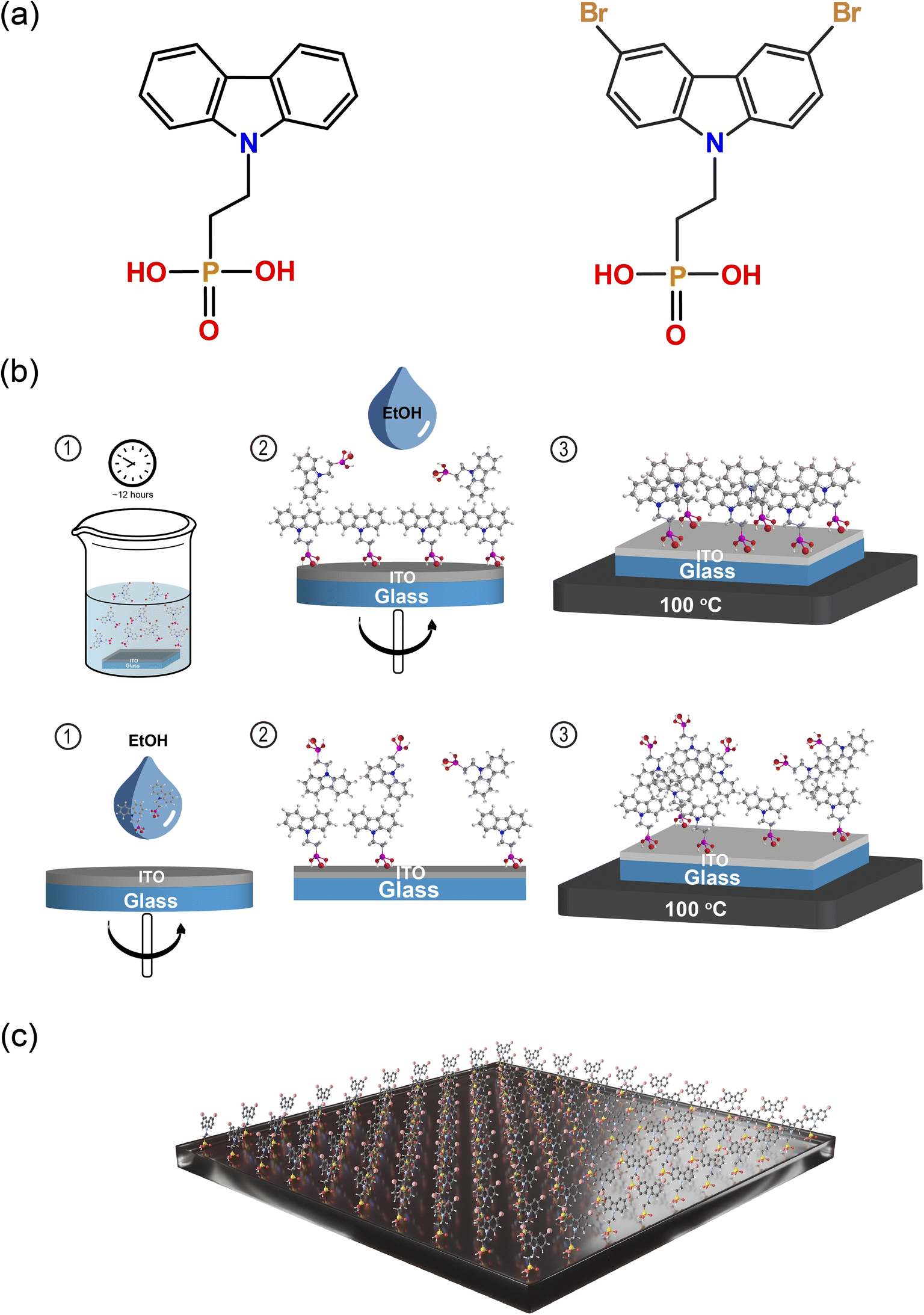 | ||
| Fig. 1 (a) Chemical structures of 2PACz (left) and Br-2PACz (right). (b) Schematic diagram of the deposition of 2PACz and Br-2PACz by liquid-phase immersion (top) and spin coating (bottom). (c) Schematic representation of the monolayer formed on an ITO substrate. | ||
First, we compare the two commonly used deposition techniques, namely liquid-phase immersion and spin-coating; the first is schematically shown in Fig. 1b.31–33 The liquid-phase immersion consists in dipping a UV-ozone pre-treated ITO substrate for 12 hours in an ethanol solution containing 0.1 mM of one of the two molecules. The phosphonic acid group reacts with the oxide (ITO) forming an ordered monolayer.34 This process is self-limited by the ITO surface and the steric hindrance of the molecule chosen.
It is reported that molecules with a phosphonic anchoring group can also form a dense layer by spin-coating.35 However, in our experience this fabrication technique does not give rise to a fully anchored monolayer. To investigate this, we performed X-ray photoelectron spectroscopy (XPS) measurements on the bare ITO substrate after SAM deposition via spin coating (2PACz), and liquid-phase immersion (Br-2PACz). The analysis of the Sn 3d 5/2 region shows the presence of Sn peaks for both bare ITO substrates and ITO with a spin-coated SAM (Fig. S1, ESI†). In contrast, the XPS spectrum for the SAM deposited via liquid-phase immersion does not exhibit any Sn peaks. Therefore, the XPS analysis confirms that the ITO substrate is fully covered when SAM molecules are deposited via liquid-phase immersion. In contrast, the spin-coating technique does not create a dense monolayer, with the presence of SAM molecules attached to the ITO surface, as shown by the presence of carbon and phosphorus atoms (C 1s, see Fig. S2a and b, ESI†). Finally, the features appearing in the Br 3d region (Fig. S2, ESI†) support the presence of bromine (Br) on the ITO/Br-2PACz sample.
Since we established that only with the liquid-phase deposition it is possible to obtain a compact monolayer, we continue to use this procedure for the rest of this work. Fig. S3 of the ESI† shows atomic force microscope (AFM) micrographs of the ITO, ITO/2PACz, and ITO/Br-2PACz samples (Fig. S3a–c, ESI†) revealing similar features with a practically unchanged surface roughness (2.26 nm, 2.32 nm, and 2.34 nm for ITO, 2PACz, and Br-2PACz, respectively). XPS measurements reveal the presence of a dense layer of carbazole-based molecules. To further investigate this molecular layer, we performed variable angle spectroscopic ellipsometry (SE) measurements (Fig. S4, ESI†). From these measurements, we calculated the mean square error (MSE) of the fit, assuming the SAM thickness to be in a range from 0 to 4 nm, and for the refractive index (n) to be in the range from 1.4 to 2.6 (Fig. S4a, ESI†).36,37 The minimum MSE value for the SAM thickness was found to be about 1 nm, while for the refractive index the minimum value is 2.2 (Fig. S4b, ESI†). It is important to note that 1 nm is indeed comparable with the molecular length of Br-2PACz (≈11 Å), which further indicates that this preparation method results in the formation of a high-quality molecular layer.
An important advantage of using a monolayer as the HTL is to reduce the amount of light that is absorbed outside the active layer. The optical absorption of ITO, and PEDOT:PSS, 2PACz, and Br-2PACz deposited on ITO substrates are shown in Fig. S5.† ITO/2PACz and ITO/Br-2PACz substrates present lower absorption (less than 1%) in the wavelength range from 370 nm to 475 nm and from 645 nm to the near infrared region when compared to an ITO/PEDOT:PSS substrate. We observed that ITO/PEDOT:PSS exhibits a lower absorption (0.6%) in the 475–650 nm range, in agreement with earlier literature.38
The effects of PEDOT:PSS, 2PACz, and Br-2PACz layers on the deposition and crystallization of the perovskite active layer was investigated with SEM, AFM, and XRD. First, the perovskite morphology was studied through SEM micrographs (Fig. 2a–c). Two parameters were selected for this analysis: the presence of pinholes and grain size. The perovskite layer deposited on PEDOT:PSS exhibits several pinholes located at the grain boundaries (Fig. 2a and S6a, ESI†). When 2PACz and Br-2PACz are used as HTLs, the perovskite layer appears more uniform and compact, with a widely reduced pinhole density (Fig. 2b, c, S6b and c, ESI†). Importantly, the grain dimension increased from 561.8 ± 5.4 nm (Fig. 2d) for the perovskite deposited on PEDOT:PSS films, to 717.6 ± 13.2 nm and 729.8 ± 12.8 nm (Fig. 2e and f) for the active layer grown on 2PACz and Br-2PACz, respectively.
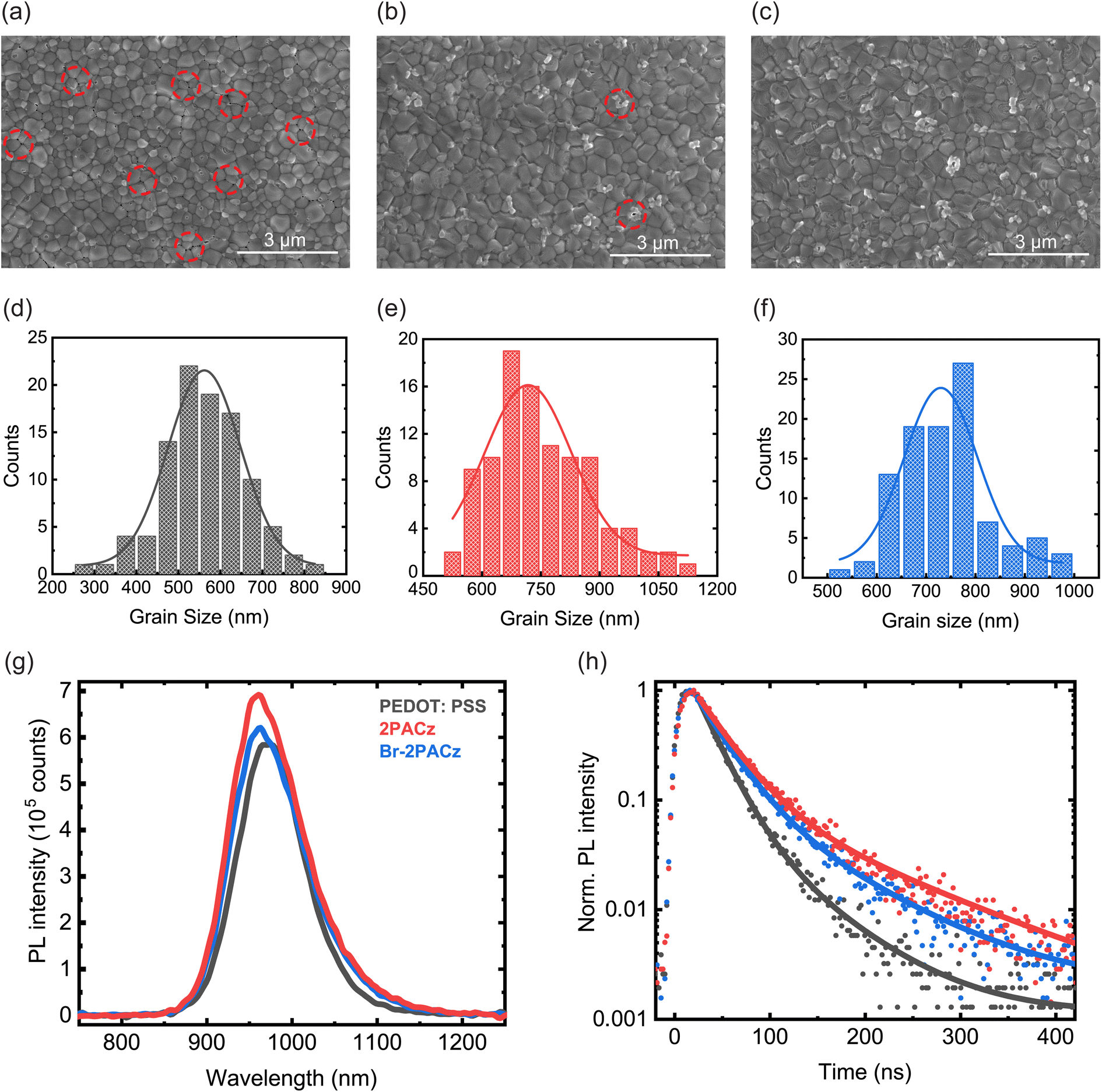 | ||
| Fig. 2 SEM micrographs of Cs0.25FA0.75Sn0.5Pb0.5I3 perovskite layers deposited on (a) PEDOT:PSS, (b) 2PACz, and (c) Br-2PACz. The red circles in (a) emphasize the presence of pinholes. Histograms showing the grain dimension distribution for the perovskite layers deposited on (d) PEDOT:PSS, (e) 2PACz, and (f) Br-2PACz. (g) Steady-state and (h) time-resolved photoluminescence of the active layer fabricated on the three different HTLs. | ||
The larger grains help to reduce the density of grain boundaries, which are places for non-radiative recombination.39 Finally, the AFM micrographs of the perovskite films confirm the better film quality when deposited on the SAMs (Fig. S7a–c, ESI†). In addition, the AFM micrographs show a slightly lower surface roughness for the perovskite deposited on the SAMs (28.66 nm and 27.14 for 2PACz and Br-2PACz, respectively) compared to that for the standard PEDOT:PSS HTL (29.81 nm).
X-ray diffraction (XRD) also confirmed the better perovskite film quality when deposited on SAMs (Fig. S8a, ESI†). We recorded a pattern with peaks located at 14.07°, 20.02°, 24.59°, 28.35°, 31.93°, and 40.67° which are assigned to (100), (110), (111), (200), (210), and (220), revealing a perovskite structure with space group Amm2.40 By comparing the (100) and (200) peak intensities for the perovskites grown on the three different HTLs (Fig. S8b and c, ESI†), we observed a higher intensity for the sample deposited on the SAMs. Specifically, Br-2PACz exhibits the highest perovskite peak intensity, revealing a film better-oriented toward (100) and (200) planes. Moreover, Cs0.25FA0.75Sn0.5Pb0.5I3 perovskite layers deposited on Br-2PACz exhibit a higher crystalline domain size (88.7 nm, calculated using the Scherrer equation) compared to the one on 2PACz (82.4 nm), and PEDOT:PSS (79.2 nm, Table S1, ESI†), in agreement with the bigger grain size observed in the SEM micrographs (Fig. 2d–f).
As shown in Fig. S9a of the ESI,† the absorption spectra of perovskite active layers deposited on the three different HTLs show a similar shape, with the active layers grown on SAMs exhibiting a slightly higher absorption in the range between 550 and 700 nm. This higher absorption is caused by the higher thickness of the perovskite thin film deposited on SAMs (400 nm) compared to the one deposited on PEDOT:PSS (340 nm). This relatively large difference is determined by the difference in surface energy between the carbazole body of the SAM and the PEDOT:PSS layer, which determines a different interaction with the perovskite precursors. This aspect is also observed in the film thickness of the perovskite active layer. In fact, the perovskite deposited on PEDOT:PSS presents a thickness of 500 nm, and 650 nm when deposited on the SAMs. The small shoulder located in the range between 975 and 1200 nm for the samples deposited on 2PACz and Br-2PACz monolayers, is attributed to the SAM absorption in the mentioned range (see inset of Fig. S9a, ESI†). Concerning the optical band gap of the perovskite layer, a negligible difference was detected with different HTLs, with all band gaps close to 1.24 eV (Fig. S9b, ESI†).
To further investigate the quality of the active layer, we performed steady-state and time-resolved photoluminescence (TRPL) measurements on ITO/HTL/perovskite samples (Fig. 2g and h). The photoluminescence (PL) intensity increases slightly for the perovskite deposited on 2PACz and Br-2PACz compared to the one deposited on PEDOT:PSS (Fig. 2g). In particular, the perovskite deposited on 2PACz shows the highest PL intensity among the three samples. A higher PL intensity suggests a reduction in non-radiative recombination, possibly due to the reduced density of traps as result of better film quality. However, the differences in PL intensity between the three samples are small, and other aspects, like the charge carrier collection at the HTL interface, could also contribute to the observed differences.41 The time-resolved PL data reported in Fig. 2h show results consistent with the steady-state PL. For all HTLs, the PL signal decays with a double exponential behavior. An initial fast charge carrier decay (τ1) is present, followed by a second slower dynamic (τ2) decay. It is important to point out that these measurements were performed by exciting the samples from the surface of the perovskite, with a wavelength of 400 nm, which is expected to be fully absorbed within the first few hundred nanometers. Therefore, we expect the measurements to initially probe the surface and bulk of the perovskite film before the carriers can diffuse to the HTL. The first rapid decay can then be related to trap-assisted recombination, which is reduced when the perovskite is deposited on 2PACz (31.10 ns) or Br-2PACz (28.27 ns), compared to on PEDOT:PSS (21.67 ns), as shown by the τ1 values in Table S2 of the ESI.† Presumably, the better perovskite quality is the main origin for the reduced trap-assisted recombination, which is well supported by the results described above. The reduced trap density is also confirmed by a limited blue shift (Fig. S10, ESI†) for the PL peak of the perovskite deposited on SAMs (960 nm and 970 nm for 2PACz/Br-2PACz and PEDOT:PSS, respectively). Generally, the non-radiative recombination assisted by trap states leads to a red shift of the PL emission, and therefore, a passivation of these intra-band gap trap states results in a blue shift.42 It is important to note that p-doping in Sn based perovskites will bring about a blue shift. However, the blue shift is accompanied by a deterioration in all the other physical parameters of the films (vide infra).43 Concerning the slower dynamic, we calculated larger values of τ2 for the perovskite deposited on ITO/SAM samples (119 ns and 85.11 ns for 2PACz and Br-2PACz, respectively) compared to PEDOT:PSS (63.85 ns). At longer delay times, the time-resolved PL measurements can become sensitive to the interaction between the perovskite and the HTL. A more efficient charge carrier transfer from the perovskite to the HTL could explain the lower value of τ2 obtained for perovskite films deposited on ITO/Br-2PACz compared to those deposited on ITO/2PACz.
At this point of our investigation, we have several reasons to expect higher performing Sn/Pb perovskite solar cells using the SAMs as the HTL. To analyze the device performance, we fabricated devices with a p-i-n architecture of the type of ITO/HTLs/perovskite/C60/BCP/Ag (Fig. 3a and S11, ESI†). Fig. 3b shows the J–V characteristics of the best devices. The best solar cell fabricated on PEDOT:PSS exhibits a power conversion efficiency (PCE) of 16.33%, with an open-circuit voltage (VOC) of 0.76 V, a short-circuit current (JSC) of 30.2 mA cm−2, and a fill factor (FF) of 0.71. The perovskite solar cells fabricated using 2PACz and Br-2PACz as HTLs display greatly improved efficiencies. The best 2PACz-based device shows an efficiency of 18.44%, a VOC of 0.8 V, a JSC of 31.1 mA cm−2, and a FF of 0.74 (Table S3, ESI†). As expected, the best device fabricated on Br-2PACz exhibits even higher performances with a PCE of 19.51%, a VOC of 0.81 V, a JSC of 32.1 mA cm−2, and a FF of 0.75. In addition, we tracked the steady-state power output for the best Br-2PACz device (Fig. S12, ESI†), which gives rise to a PCE of 19.12%, which is in good agreement with the value obtained from the J–V scan.
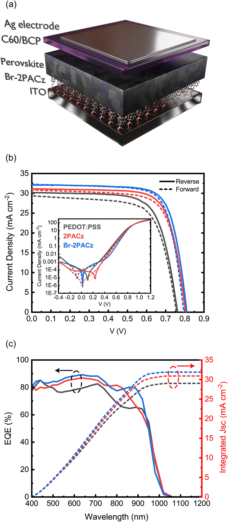 | ||
| Fig. 3 (a) Schematic representation of the p-i-n structures used for the solar cells. (b) Current density–voltage (J–V) characteristics measured under AM 1.5G illumination for PEDOT:PSS-(black lines), 2PACz-(red lines), and Br-2PACz-(blue lines) based devices. The solid lines show the reverse-bias measurements, while the dashed lines display the forward-bias measurements. (c) External quantum efficiency (EQE) versus wavelength and the corresponding integrated current for the three different fabricated solar cells. | ||
The higher VOC, JSC, and FF of the devices fabricated on SAMs can be explained by the higher crystallinity and overall improved quality of the perovskite layers. However, there is also a noticeable difference between the two SAMs. In fact, the solar cells fabricated on the Br-2PACz HTL exhibit higher values for every device metric compared to those fabricated on the 2PACz-based devices. This is consistent with the improved perovskite properties on these SAMs and furthermore could be because the Br can passivate halogen vacancies of the buried interface.
The inset of Fig. 3b shows the dark J–V characteristics for the three types of devices. The one for PEDOT:PSS based devices presents poor diode behavior and a high leakage current, as can be expected for the perovskite film showing the highest pinhole density and poorest crystallinity. The dark characteristics of devices fabricated using SAMs show much better diode behavior with a lower leakage current, which is again an indication of the higher quality of the active layers. However, the dark J–V characteristics of solar cells fabricated on PEDOT:PSS and 2PACz exhibit a large hysteresis. This is largely different from what is happening in devices using Br-2PACz, which show a hysteresis-free behavior. These better dark characteristics are determined by the much lower trap density present at the Br-2PACz/perovskite interface, which is due to the healing effect of the Br atom. Finally, Fig. 3c shows the external quantum efficiency (EQE) spectra, revealing the integrated currents for the three different devices fabricated with PEDOT:PSS, 2PACz, and Br-2PACz as the HTL to be 29.04, 30.92, and 31.91 mA cm−2, respectively, which agree well with the currents obtained from the J–V characteristics. We notice some differences in the shapes of the EQE graphs for the different devices, which could be due to the differences in their thickness and relative cavity effects (vide infra). However, the lower trap density present at the buried interface of the active layer deposited on Br-2PACz could also be a reason for the difference measured at the band-gap edge.
Fig. 4a–d show a statistical analysis of the data obtained from 20 devices for each type of sample. The average values confirm what has been previously mentioned for the best devices, namely that the samples fabricated with Br-2PACz as the HTL show the highest PCE with an average value of 19.1 ± 0.35% (Fig. 4d), and an overall improvement in all device parameters (Fig. 4a–c). In addition to the better efficiency, solar cells fabricated on SAMs show a better reproducibility compared to the ones on PEDOT:PSS. Considering the poor wettability of mixed Sn/Pb or pure Sn perovskite solution on the carbazole molecular layer, this represents a counterintuitive result. Indeed, the perovskite layer does not fully cover the SAM if a normal spin coating procedure is utilized, and this strongly affects the device reproducibility (Fig. S13 and Table S4, ESI†). To avoid any influence on our statistical analysis, we developed a deposition technique where the perovskite solution is manually spread to get full substrate coverage before the activation of the spin coater. While this technique is far from being ideal for device fabrication, it does allow us to compare the performance of the HTLs on the same footing. The XRD analysis reveals that this deposition method does not influence perovskite crystal growth and quality (Fig. S14, ESI†).
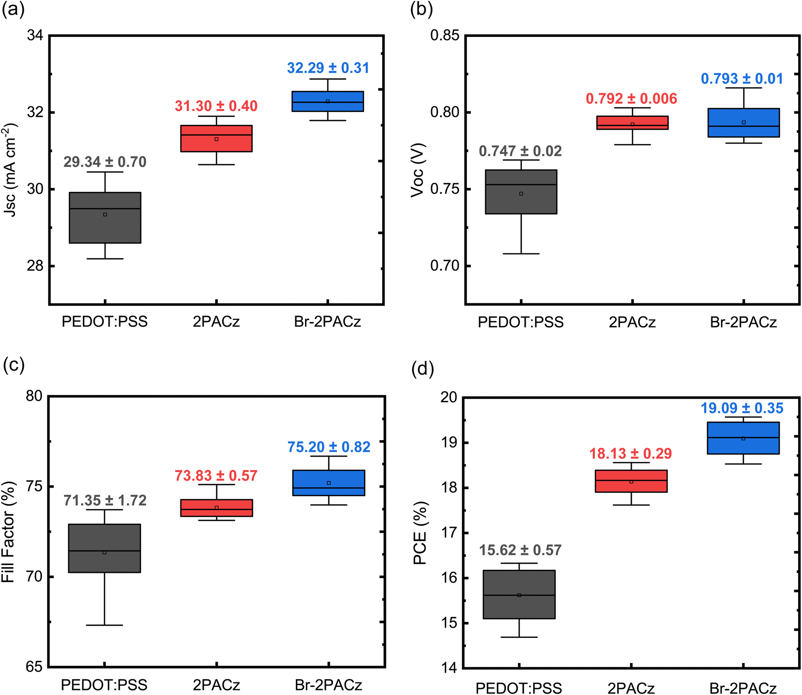 | ||
| Fig. 4 Statistical analysis performed on 20 devices fabricated with PEDOT:PSS (black boxes), 2PACz (red boxes), and Br-2PACz (blue boxes) as the HTL. Data for the (a) JSC, (b) VOC, (c) FF, and (d) PCE are reported. | ||
Going deeper in solar cell characterization, we investigated the light-intensity dependence of VOC and JSC, as shown in Fig. S15, ESI.† From the VOC behavior, we observed a lower slope for the devices fabricated on SAMs with respect to PEDOT:PSS (Fig. S15, ESI†). This lower slope underlies the suppressed trap-assisted recombination, which is especially reduced for the Br-2PACz-based devices. This is a strong reason for the improved VOC.44 Ultimately, the improved VOC could be assigned to a better energy alignment between the HTL HOMO level and the perovskite valence band. To prove this, we measured the work function (WF) values of the HTLs investigated using Kelvin-probe force microscopy (KPFM) (Fig. S16a and b, ESI†). The entire KPFM analysis has been performed in air, which is the reason for the marginally different values obtained when compared to the literature.25 The bare ITO surface has a measured WF of −4.71 eV. When the ITO surface is covered with a PEDOT:PSS film or 2PACz monolayer, the WF value decreases to −4.97 eV and −4.83 eV, respectively. On the other hand, the ITO/Br-2PACz electrode presents a further increase of the WF value (−5.28 eV), which we attribute to the effect of Br functionalization. The ITO/Br-2PACz electrode shows a WF value closer to the perovskite valence band, which could be another reason for the improved VOC.
The charge recombination was further investigated with impedance spectroscopy under open-circuit and dark conditions (Fig. S17a and S18, ESI†). PEDOT:PSS-based devices presented two different semicircles fitted by two RC components, as shown in Fig. S18 of the ESI.† The small low-frequency arch describes the recombination in the HTL (RHTL), while the larger high-frequency semicircle is related to the recombination that occurs in the perovskite bulk (Rrec).45 The 2PACz-based devices also exhibit two arches. However, for this sample, the low-frequency semicircle presents negative impedance values, probably linked to ion accumulation at the perovskite/HTL interface.46,47 In contrast, devices fabricated using Br-2PACz as the HTL only exhibit an arch, revealing a widely reduced recombination at the perovskite/HTL interface. To better estimate the recombination in the perovskite bulk and at the HTL/perovskite interface, we compared the value for the RHTL and Rrec for the three different devices (Table S5, ESI†). From this table it is clear that the Rrec values increase going from PEDOT:PSS to 2PACz and to Br-2PACz, revealing reduced charge recombination in the perovskite bulk when Br-2PACz is used as the HTL. Moreover, the charge recombination at the HTL/perovskite interface is reduced when 2PACz is used, and completely removed when Br-2PACz is implemented as revealed by the absence of the low frequency arch. This finding supports the fact that the buried interface on the Br-2PACz sample is much less defective due to the ability of Br to partially passivate halide vacancies.
Finally, Mott–Schottky analysis (Fig. S17b, ESI†) reveals a decrease in background charge-carrier density from 1.73 × 1016 cm−3 for PEDOT:PSS to 1.27 × 1016 cm−3 for SAM-based solar cells. The background charge-carrier density is mainly caused by self p-doping due to Sn2+ oxidation. The reduction of the background charge-carrier density in the SAM HTL samples is certainly due to the higher crystallinity.43
To conclude our investigation, we studied the stability of the fabricated solar cells. First, we analyzed the device behavior under ambient conditions at room temperature (21 °C, 40% RH, Fig. 5a); then we investigated the thermal stability (85 °C, N2 atmosphere) (Fig. 5b) for both non-encapsulated devices, and finally, we studied the operation stability under AM 1.5G for encapsulated devices in air (Fig. 5c). The devices fabricated using the SAMs exhibit higher stability with respect to those using PEDOT:PSS under all the studied conditions. In addition, we observe a negligible difference between the two SAMs, where Br-2PACz shows better performance. Specifically, when stored in air (21 °C, 40% RH), the PEDOT:PSS-based device exhibits a fast decay, losing half of its initial efficiency after 10 hours (Fig. 5a). In contrast, the 2PACz- and Br-2PACz-based devices show a much slower decay, with a small difference between the fresh device and the one stored in air for 10 hours. The poor air stability for the PEDOT:PSS-based device is attributed to its hygroscopic and acidic nature, which rapidly degrades the perovskite active layer.48 On the other hand, 2PACz and Br-2PACz molecules are hydrophobic, and repel water molecules. This is one of the possible and most plausible reasons for the drastically improved air stability of these devices. The thermal stability of the solar cells confirmed the results of the air stability study (Fig. 5b). Fig. 5c shows impressive results for stability under working conditions of mixed Sn/Pb-based perovskite solar cells with devices fabricated with Br-2PACz and 2PACz, maintaining 92% and 89% of their initial PCE after 72 hours. The device using PEDOT:PSS retains only 79% of its initial PCE after the same period. Importantly, solar cells using Br-2PACz HTL show an efficiency 80% of their initial efficiency (T80 lifetime) after 230 h of operation. This result exceeds the literature record device for mixed Sn/Pb perovskite solar cells (T80 after around 215 h).12 The higher stability for the SAM-based devices could be explained by the slower Sn2+ oxidation in this sample with respect to the one using PEDOT:PSS as the HTL, as has been recently suggested.33 Finally, our shelf-lifetime in a N2 atmosphere is presented in Fig. 5d. This measurement also confirms the widely improved stability when the SAMs are implemented as HTLs. Solar cells with Br-2PACz retain 80.2% of their efficiency after 176 days (4224 h), while PEDOT:PSS exhibits a faster decay and a higher PCE decrease after only 42 days.
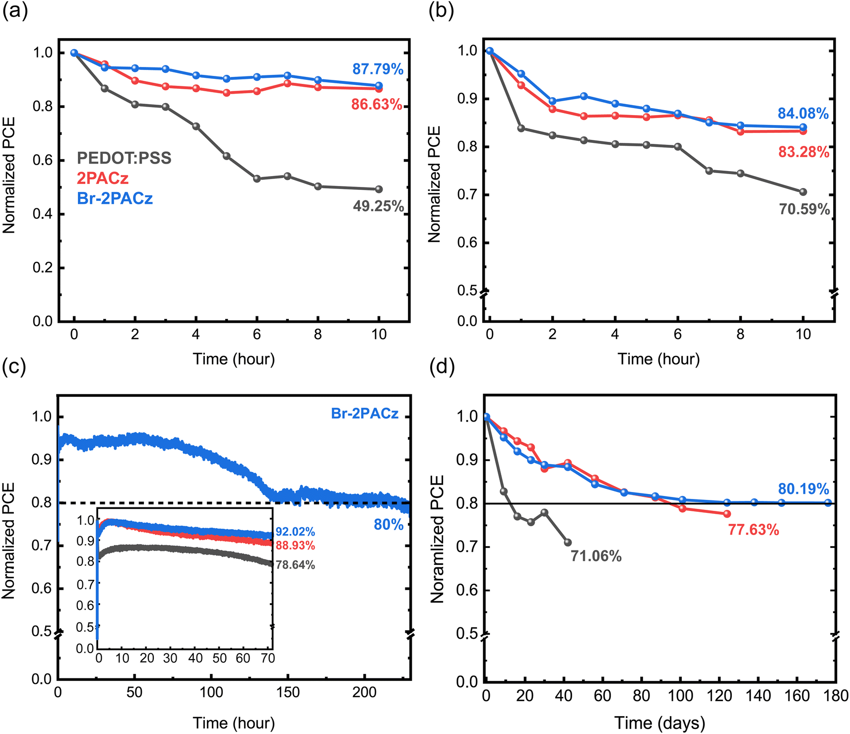 | ||
| Fig. 5 Stability of the three different devices using PEDOT:PSS (black curves), 2PACz (red curves), and Br-2PACz (blue curves) s HTLs measured (a) under ambient conditions (21 °C, 40% RH); (b) at high temperature (85 °C, N2 atmosphere); (c) under operation in AM 1.5G (encapsulated device in air); and (d) in a shelf-life time test (N2 atmosphere, dark condition). | ||
3. Conclusion
We have used two different carbazole based SAMs as the HTL in Sn/Pb perovskite solar cells using Cs0.25FA0.75Sn0.5Pb0.5I3 as the active layer. By using Br-2PACz as the HTL we achieved a PCE of 19.51% without any anti-reflective coating or doping for the HTL. This result represents the first successful attempt of implementing a halogenated SAM in an MA-free perovskite solar cell, achieving one of the highest device performances (Fig. S19, ESI†). 80.2% of the device efficiency is maintained after 176 days (4224 h) in a glove box. This result demonstrates that the halogen functionalization of the SAMs is an efficient way to improve both the device performance and stability. Several factors seem to determine these improvements. The two carbazole-based molecules are able to form a self-assembled monolayer which shows minimal parasitic absorption and low charge recombination when compared to PEDOT:PSS films. Additionally, depositing the perovskite layer on the SAM results in higher crystallinity, with reduced pinhole density and larger grains. The defect density of the perovskite films was also reduced when deposited on Br-2PACz or 2PACz compared to on PEDOT:PSS. PL and TRPL measurements further confirmed the better perovskite film quality when deposited on a SAM, with reduced charge recombination and enhanced charge transfer for Br-2PACz compared to PEDOT:PSS. Finally, the wettability of the perovskite precursor solution on top of the SAM is a problem which could limit the application of SAMs in Sn or mixed Sn/Pb perovskite solar cells. A solution for this issue may allow the improvement of both the scalability and reproducibility of the SAM-based perovskite solar cell.4. Experimental section
4.1 Materials
Poly(3,4-ethylenedioxythiophene) polystyrene sulfonate (PEDOT:PSS) in a water dispersion (Clevios VP Al 4083) was purchased from Heraeus. [2-(9H-Carbazol-9-yl)ethyl]phosphonic acid (2PACz) and [2-(3,6-dibromo-9H-carbazol-9-yl)ethyl]phosphonic acid (Br-2PACz) were acquired from Dyenamo. Formamidinium iodide (FAI, >98%) and bathocuproine (BCP, >99%) were bought from TCI EUROPE N. V. Tin(II) iodide (SnI2, 99.999%), tin(II) fluoride (SnF2, 99%), cesium iodide (CsI, 99.999%), dimethylformamide (DMF, 99.8%), anisole (anhydrous, 99.7%), and buckminsterfullerene (C60, 99.9%) were purchased from Sigma Aldrich. Lead(II) iodide (PbI2, 99.999%), and dimethyl sulfoxide (DMSO, 99.8+%) were acquired from Alfa Aesar. Ethanol (EtOH, 99.5%) was acquired from Thermo Fisher Scientific. Finally, silver rods (Ag, 99.99%) were purchased from Umicore.4.2 Perovskite deposition
The perovskite solution (1.4 M) was prepared by dissolving FAI (1.05 mmol), CsI (0.35 mmol), SnI2 (0.7 mmol), PbI2 (0.7 mmol), and SnF2 (0.07 mmol) in 800 µl of DMF and 200 µl of DMSO. The solution was continuously stirred for 3 hours and filtered using 0.2 µm PTFE membrane capsules. Next, the perovskite solution was spin coated on ITO/HTLs substrates at 4000 rpm for 80 s in a N2-filled glovebox with O2 and H2O concentrations of <0.1 ppm. Anisole (250 µl) was used as the antisolvent and dropped 25 s after the start of the spinning process. The perovskite films were immediately annealed at 120 °C for 10 min.4.3 Device fabrication
30 × 30 mm2 patterned ITO substrates were washed using a soapy water solution (soap![[thin space (1/6-em)]](https://www.rsc.org/images/entities/char_2009.gif) :water 1:9) and subsequently sonicated in deionized water, acetone, and isopropyl alcohol for 20 minutes each. Then, the substrates were dried in air at 130 °C to remove excess IPA. After the drying procedure, the ITO substrates were transferred to a UV-ozone chamber for 30 min. For the PEDOT:PSS-based devices, a PEDOT:PSS layer has been spin coated at 3000 rpm for 60 s and annealed at 140 °C for 20 min. For the SAM-based solar cells, the ITO substrates were transferred to a N2 filled glovebox and dipped in a sonicated (30 min) EtOH solution (30 ml), where 0.1 mM of 2PACz or Br-2PACz was dissolved. The ITO substrates were left in the EtOH solution for around 12 hours. Later, the substrates were dried using a spin coater machine at 3000 rpm for 30 s and further dried at 100 °C for 2 minutes. After this process, on the ITO substrate there is a SAM with several aggregated molecules. To remove these agglomerates, we proceeded to wash the monolayer. EtOH solution (200 µl) was dynamically spin coated on ITO/SAM at 3000 rpm for 30 s to remove the aggregates, and the substrates were annealed at 100 °C for 1 min. For the functionalized carbazole molecules deposited via spin coating, we prepared a solution of the carbazole derivatives in ethanol (1 mM), which was stirred overnight. The carbazole derivative solution was spin coated on UV-treated ITO substrates at 3000 rpm for 30 s. Before starting the spin coating procedure, we left the SAM solution to react with ITO for 1 min. Then, the ITO substrates were annealed for 10 min at 100 °C. Next, the perovskite layer was deposited as previously described. Finally, all the substrates were transferred to a vacuum chamber where 30 nm of C60, 6 nm of BCP, and 100 nm of Ag were evaporated under a pressure of 10−7 mbar.
:water 1:9) and subsequently sonicated in deionized water, acetone, and isopropyl alcohol for 20 minutes each. Then, the substrates were dried in air at 130 °C to remove excess IPA. After the drying procedure, the ITO substrates were transferred to a UV-ozone chamber for 30 min. For the PEDOT:PSS-based devices, a PEDOT:PSS layer has been spin coated at 3000 rpm for 60 s and annealed at 140 °C for 20 min. For the SAM-based solar cells, the ITO substrates were transferred to a N2 filled glovebox and dipped in a sonicated (30 min) EtOH solution (30 ml), where 0.1 mM of 2PACz or Br-2PACz was dissolved. The ITO substrates were left in the EtOH solution for around 12 hours. Later, the substrates were dried using a spin coater machine at 3000 rpm for 30 s and further dried at 100 °C for 2 minutes. After this process, on the ITO substrate there is a SAM with several aggregated molecules. To remove these agglomerates, we proceeded to wash the monolayer. EtOH solution (200 µl) was dynamically spin coated on ITO/SAM at 3000 rpm for 30 s to remove the aggregates, and the substrates were annealed at 100 °C for 1 min. For the functionalized carbazole molecules deposited via spin coating, we prepared a solution of the carbazole derivatives in ethanol (1 mM), which was stirred overnight. The carbazole derivative solution was spin coated on UV-treated ITO substrates at 3000 rpm for 30 s. Before starting the spin coating procedure, we left the SAM solution to react with ITO for 1 min. Then, the ITO substrates were annealed for 10 min at 100 °C. Next, the perovskite layer was deposited as previously described. Finally, all the substrates were transferred to a vacuum chamber where 30 nm of C60, 6 nm of BCP, and 100 nm of Ag were evaporated under a pressure of 10−7 mbar.
4.4 Film characterization
X-ray photoelectron spectroscopy (XPS) was performed using a PHI Quantera II ESCA spectrometer from Physical Electronics. A monochromatic Al Kα X-ray source with an output energy of 25 W (15 kV) was used. The band-pass energy for the survey was 112 eV and for the element characterization 69 eV. Scanning electron microscopy (SEM) images were recorded using a Nova NanoSEM 650 with an acceleration voltage of 5 kV. The cross-section measurements were performed using a LEO 1530 FEG scanning electron microscopy instrument (LEO Electron Microscopy Ltd, Cambridge, UK) with an in-lens detector operating at 3 kV. The absorption spectrum of the films without encapsulation was recorded using a Shimatzu UV-vis-NIR spectrophotometer (UV 3600). We used a Bruker Multimode 8 microscope with ScanAsyst air probes (resonant frequency 70 kHz and spring constant 0.4 N m−1) to perform atomic force microscopy (AFM) of the perovskite and monolayer morphology. The AFM images were recorded using a scan rate of 0.912 Hz with a resolution of 1024 samples per line. The data were later analyzed with Gwyddion-free scanning probe microscope data analysis software. For the Kelvin-probe force microscopy (KPFM) measurements, we used SCM-PIT-V2 tips (resonant frequency 75 kHz and spring constant 3 N m−1) and the electrical & magnetic lift modes/surface potential (FM-KPFM). The measurements were performed using a drive frequency of 75.9 kHz and an amplitude frequency of 55.5 mV. To determine the sample work function, we need to know the work function of the tip. For this purpose, we used freshly cleaved highly ordered pyrolytic graphite (HOPG) whose work function is about 4.6 eV. The ellipsometry measurements were carried out using a UV-vis ellipsometer M2000, from J. A. Woollam Co., using the commercial software WVase32® to collect and analyze the data. Prior to the measurement, the system was calibrated using a known optical constant substrate (27 nm of SiO2 on a Si wafer). Then, the measurements were performed at incident angles from 70 to 75° and the data were modeled using a Cauchy dispersion formula in a wavelength range from 350 to 1700 nm. The silicon substrates used (back side etched and front side polished) were covered with a native oxide, whose thickness (1.6 nm) was individually measured for each sample used, for an accurate fitting. The chemical interaction between the phosphonic acid group and the oxide from either the Si wafer or ITO substrate is identical. For this reason, we can assume that the characterization made on a Si wafer can be translated to the ITO substrate. The spectroscopic ellipsometry (SE) measurements were performed after every layer deposition step to ensure a correct fitting of the individual thicknesses. This meant that SE data were collected for native oxide substrates alone and on the substrate covered with SAMs (Br-2PACz). X-ray diffraction (XRD) patterns were recorded on perovskite films without encapsulation in air using a Bruker D8 Advance X-ray diffractometer with a Cu Ka source (λ = 1.54 Å) and a Lynxeye detector. Steady-state and time-resolved photoluminescence (PL) measurements were performed in reflection geometry, exciting the samples from the surface of the perovskite (top side). A wavelength of 400 nm was obtained as second harmonic of a mode-locked Ti:sapphire laser (Coherent Mira 900). The laser repetition rate of 76 MHz was reduced through an optical pulse picker to extend the time range in the time-resolved measurements and to allow for complete charge carrier relaxation after each laser pulse. All the measurements were performed with a fluence of about 4.2 µJ cm−2 per pulse. Steady-state spectra were acquired using a Hamamatsu spectral-calibrated EM-CCD camera. Time-resolved PL traces were recorded with a Hamamatsu streak camera, in a single-sweep mode. The samples were mounted in a sealed sample holder and kept in a nitrogen atmosphere during the measurements.4.5 Device characterization
The device J–V curves were measured in a N2-filled glovebox (O2 < 0.1 ppm and H2O < 0.1 ppm) using a Keithley 2400 source meter and a Steuernagel Solar constant 1200 metal halide lamp. To perform the measurements under the standard test condition (295 K, AM 1.5G solar illumination), we used a Si reference cell. A shadow mask (0.04 cm2) was used to exclude lateral contributions beyond the device area. A home-built setup was used for measuring the external quantum efficiency (EQE) of the solar cells. The setup is described in our previous work.49 The final integrated JSC value was multiplied by the mismatch factor (1.07) due to the small difference between the spectral response of the silicon and perovskite solar cells. We performed the capacitance–voltage (C–V) measurements using a Solartron 1260 gain-phase analyzer. The measurements were conducted under dark conditions, applying an AC drive voltage of 40 mV with a fixed frequency of 10 kHz. The applied DC bias was swept from −0.9 V to 0.9 V. For impedance spectroscopy, the frequency was swept in a range from 0.1 Hz to 1 MHz, while the device was kept under open-circuit conditions. For the operation stability under AM 1.5G, we encapsulated the device by covering the solar cells with 20 nm of Al2O3 deposited by atomic layer deposition at 60 °C.Conflicts of interest
There are no conflicts to declare.Acknowledgements
We kindly acknowledge A. Kamp for the technical support and for designing the device structure. We acknowledge Dyenamo for providing the SAMs utilized in this study. This publication is part of the Netherlands Organization for Scientific Research (NWO)-Focus Group “Next Generation Organic Photovoltaics”, participating in the Dutch Institute for Fundamental Energy Research (DIFFER). This work was partially funded by the European Union's Horizon 2020 program, through a FET Proactive Research and Innovation Action under grant agreement no. 101084124 (DIAMOND). E. M. J. Johansson acknowledges financial support from the Swedish Energy Agency.References
- H. Min, D. Y. Lee, J. Kim, G. Kim, K. S. Lee, J. Kim, M. J. Paik, Y. K. Kim, K. S. Kim, M. G. Kim, T. J. Shin and S. Il Seok, Nature, 2021, 598, 444 CrossRef CAS PubMed.
- K. Yoshikawa, H. Kawasaki, W. Yoshida, T. Irie, K. Konishi, K. Nakano, T. Uto, D. Adachi, M. Kanematsu, H. Uzu and K. Yamamoto, Nat. Energy, 2017, 2, 17032 CrossRef CAS.
- P. Roy, N. Kumar Sinha, S. Tiwari and A. Khare, Sol. Energy, 2020, 198, 665–688 CrossRef CAS.
- J. S. Manser, J. A. Christians and P. V. Kamat, Chem. Rev., 2016, 116, 12956–13008 CrossRef CAS PubMed.
- E. L. Unger, L. Kegelmann, K. Suchan, D. Sörell, L. Korte and S. Albrecht, J. Mater. Chem. A, 2017, 5, 11401–11409 RSC.
- W. Schockley, J. Appl. Phys., 1961, 32, 1402 CrossRef.
- R. Prasanna, A. Gold-Parker, T. Leijtens, B. Conings, A. Babayigit, H. G. Boyen, M. F. Toney and M. D. McGehee, J. Am. Chem. Soc., 2017, 139, 11117–11124 CrossRef CAS PubMed.
- S. Kahmann, Z. Chen, O. Hordiichuk, O. Nazarenko, S. Shao, M. V. Kovalenko, G. R. Blake, S. Tao and M. A. Loi, ACS Appl. Mater. Interfaces, 2022, 14, 34253–34261 CrossRef CAS PubMed.
- M. Jošt, L. Kegelmann, L. Korte and S. Albrecht, Adv. Energy Mater., 2020, 10, 1904102 CrossRef.
- A. Filippetti, S. Kahmann, C. Caddeo, A. Mattoni, M. Saba, A. Bosin and M. A. Loi, J. Mater. Chem. A, 2021, 9, 11812–11826 RSC.
- M. H. Futscher and B. Ehrler, ACS Energy Lett., 2016, 1, 863–868 CrossRef CAS.
- S. Hu, K. Otsuka, R. Murdey, T. Nakamura, M. A. Truong, T. Yamada, T. Handa, K. Matsuda, K. Nakano, A. Sato, K. Marumoto, K. Tajima, Y. Kanemitsu and A. Wakamiya, Energy Environ. Sci., 2022, 15, 2096 RSC.
- J. Cameron and P. J. Skabara, Mater. Horiz., 2020, 7, 1759–1772 RSC.
- M. Jørgensen, K. Norrman and F. C. Krebs, Sol. Energy Mater. Sol. Cells, 2008, 92, 686–714 CrossRef.
- M. Kim, M. Yi, W. Jang, J. K. Kim and D. H. Wang, Polymers, 2020, 12, 129 CrossRef CAS PubMed.
- J. Werner, T. Moot, T. A. Gossett, I. E. Gould, A. F. Palmstrom, E. J. Wolf, C. C. Boyd, M. F. A. M. Van Hest, J. M. Luther, J. J. Berry and M. D. McGehee, ACS Energy Lett., 2020, 5, 1215–1223 CrossRef CAS.
- Q. Han, Y. Wei, R. Lin, Z. Fang, K. Xiao, X. Luo, S. Gu, J. Zhu, L. Ding and H. Tan, Sci. Bull., 2019, 64, 1399–1401 CrossRef PubMed.
- S. Shao, Y. Cui, H. Duim, X. Qiu, J. Dong, G. H. Brink, G. Portale, R. C. Chiechi, S. Zhang, J. Hou and M. A. Loi, Adv. Mater., 2018, 30, 1803703 CrossRef PubMed.
- A. Al-Ashouri, A. Magomedov, M. Roß, M. Jošt, M. Talaikis, G. Chistiakova, T. Bertram, J. A. Márquez, E. Köhnen, E. Kasparavičius, S. Levcenco, L. Gil-Escrig, C. J. Hages, R. Schlatmann, B. Rech, T. Malinauskas, T. Unold, C. A. Kaufmann, L. Korte, G. Niaura, V. Getautis and S. Albrecht, Energy Environ. Sci., 2019, 12, 3356–3369 RSC.
- W. Gao, L. Dickinson, C. Grozinger, F. G. Morin and L. Reven, Langmuir, 1996, 12, 6429–6435 CrossRef CAS.
- R. Quiñones, A. Raman and E. S. Gawalt, Thin Solid Films, 2008, 516, 8774–8781 CrossRef.
- X. Deng, F. Qi, F. Li, S. Wu, F. R. Lin, Z. Zhang, Z. Guan, Z. Yang, C. S. Lee and A. K. Y. Jen, Angew. Chem. Int. Ed., 2022, 61, e202203088 CAS.
- S. Y. Kim, S. J. Cho, S. E. Byeon, X. He and H. J. Yoon, Adv. Energy Mater., 2020, 10, 2002606 CrossRef CAS.
- G. Kapil, T. Bessho, Y. Sanehira, S. R. Sahamir, M. Chen, A. K. Baranwal, D. Liu, Y. Sono, D. Hirotani, D. Nomura, K. Nishimura, M. A. Kamarudin, Q. Shen, H. Segawa and S. Hayase, ACS Energy Lett., 2022, 7, 966–974 CrossRef CAS.
- Y. Lin, A. Magomedov, Y. Firdaus, D. Kaltsas, A. El-Labban, H. Faber, D. R. Naphade, E. Yengel, X. Zheng, E. Yarali, N. Chaturvedi, K. Loganathan, D. Gkeka, S. H. AlShammari, O. M. Bakr, F. Laquai, L. Tsetseris, V. Getautis and T. D. Anthopoulos, ChemSusChem, 2021, 14, 3569–3578 CrossRef CAS PubMed.
- Y. Lin, Y. Zhang, J. Zhang, M. Marcinskas, T. Malinauskas, A. Magomedov, M. I. Nugraha, D. Kaltsas, D. R. Naphade, G. T. Harrison, A. El-labban, S. Barlow, S. De Wolf, E. Wang, I. Mcculloch, L. Tsetseris, V. Getautis, S. R. Marder and T. D. Anthopoulos, Adv. Energy Mater., 2022, 12, 2202503 CrossRef CAS.
- J. Wang, Z. Yu, D. D. Astridge, Z. Ni, L. Zhao, B. Chen, M. Wang, J. Zhou, G. Yang, X. Dai, A. Sellinger and J. Huang, ACS Energy Lett., 2022, 7, 3353–3361 CrossRef CAS.
- S. Tan, T. Huang and Y. Yang, JPhys Energy, 2021, 3, 042003 CrossRef CAS.
- J. Y. Lee, S. Y. Kim and H. J. Yoon, Adv. Opt. Mater., 2022, 10, 2101361 CrossRef CAS.
- N. Jia, P. Guo, K. Zhang, C. Liu, R. Chen, Z. Liu, Q. Ye and H. Wang, ACS Sustain. Chem. Eng., 2022, 10, 16359–16367 CrossRef.
- D. Zhang, H. Zhang, H. Guo, F. Ye, S. Liu and Y. Wu, Adv. Funct. Mater., 2022, 32, 2200174 CrossRef CAS.
- J. Dagar, M. Fenske, A. Al-Ashouri, C. Schultz, B. Li, H. Köbler, R. Munir, G. Parmasivam, J. Li, I. Levine, A. Merdasa, L. Kegelmann, H. Näsström, J. A. Marquez, T. Unold, D. M. Többens, R. Schlatmann, B. Stegemann, A. Abate, S. Albrecht and E. Unger, ACS Appl. Mater. Interfaces, 2021, 13, 13022–13033 CrossRef CAS PubMed.
- G. Kapil, T. Bessho, Y. Sanehira, S. R. Sahamir, M. Chen, A. K. Baranwal, D. Liu, Y. Sono, D. Hirotani, D. Nomura, K. Nishimura, M. A. Kamarudin, Q. Shen, H. Segawa and S. Hayase, ACS Energy Lett., 2022, 7, 966–974 CrossRef CAS.
- S. Casalini, C. A. Bortolotti, F. Leonardi and F. Biscarini, Chem. Soc. Rev., 2017, 46, 40–71 RSC.
- R. F. Dou, X. C. Ma, L. Xi, H. L. Yip, K. Y. Wong, W. M. Lau, J. F. Jia, Q. K. Xue, W. S. Yang, H. Ma and A. K. Y. Jen, Langmuir, 2006, 22, 3049–3056 CrossRef CAS PubMed.
- N. Phung, M. Verheijen, A. Todinova, K. Datta, M. Verhage, A. Al-Ashouri, H. Köbler, X. Li, A. Abate, S. Albrecht and M. Creatore, ACS Appl. Mater. Interfaces, 2022, 14, 2166–2176 CrossRef CAS PubMed.
- M. Prato, R. Moroni, F. Bisio, R. Rolandi, L. Mattera, O. Cavalleri and M. Canepa, J. Phys. Chem. C, 2008, 112, 3899–3906 CrossRef CAS.
- H. Choi, C. K. Mai, H. B. Kim, J. Jeong, S. Song, G. C. Bazan, J. Y. Kim and A. J. Heeger, Nat. Commun., 2015, 6, 7348 CrossRef CAS PubMed.
- T. S. Sherkar, C. Momblona, L. Gil-Escrig, J. Ávila, M. Sessolo, H. J. Bolink and L. J. A. Koster, ACS Energy Lett., 2017, 2, 1214–1222 CrossRef CAS PubMed.
- G. E. Eperon, T. Leijtens, K. A. Bush, R. Prasanna, T. Green, J. T. W. Wang, D. P. McMeekin, G. Volonakis, R. L. Milot, R. May, A. Palmstrom, D. J. Slotcavage, R. A. Belisle, J. B. Patel, E. S. Parrott, R. J. Sutton, W. Ma, F. Moghadam, B. Conings, A. Babayigit, H. G. Boyen, S. Bent, F. Giustino, L. M. Herz, M. B. Johnston, M. D. McGehee and H. J. Snaith, Science, 2016, 354, 861–865 CrossRef CAS PubMed.
- J. H. Lee, I. S. Jin, Y. W. Noh, S. H. Park and J. W. Jung, ACS Sustain. Chem. Eng., 2019, 7, 17636–17642 CrossRef.
- Y. Shao, Z. Xiao, C. Bi, Y. Yuan and J. Huang, Nat. Commun., 2014, 5, 5748 CrossRef PubMed.
- S. Kahmann, S. Shao and M. A. Loi, Adv. Funct. Mater., 2019, 29, 1902963 CrossRef.
- D. Yang, X. Zhou, R. Yang, Z. Yang, W. Yu, X. Wang, C. Li, S. Liu and R. P. H. Chang, Energy Environ. Sci., 2016, 9, 3071–3078 RSC.
- E. Von Hauff and D. Klotz, J. Mater. Chem. C, 2022, 10, 742–761 RSC.
- I. Zarazua, J. Bisquert and G. Garcia-Belmonte, J. Phys. Chem. Lett., 2016, 7, 525–528 CrossRef CAS PubMed.
- F. Ebadi, N. Taghavinia, R. Mohammadpour, A. Hagfeldt and W. Tress, Nat. Commun., 2019, 10, 1574 CrossRef PubMed.
- Q. Wang, C. C. Chueh, M. Eslamian and A. K. Y. Jen, ACS Appl. Mater. Interfaces, 2016, 8, 32068–32076 CrossRef CAS PubMed.
- M. Pitaro, R. Pau, H. Duim, M. Mertens, W. T. M. Van Gompel, G. Portale, L. Lutsen and M. A. Loi, Appl. Phys. Rev., 2022, 9, 021407 CAS.
Footnote |
| † Electronic supplementary information (ESI) available. See DOI: https://doi.org/10.1039/d3ta01276j |
| This journal is © The Royal Society of Chemistry 2023 |