
Stability and efficiency improvement of perovskite solar cells by surface hydroxyl defect passivation of SnO2 layer with 4-fluorothiophenol†
Yun-Sung
Jeon
 a,
Dong-Ho
Kang
a,
Jeong-Hyeon
Kim
a and
Nam-Gyu
Park
*ab
a,
Dong-Ho
Kang
a,
Jeong-Hyeon
Kim
a and
Nam-Gyu
Park
*ab
aSchool of Chemical Engineering and Center for Antibonding Regulated Crystals, Sungkyunkwan University, Suwon 16419, Republic of Korea. E-mail: npark@skku.edu
bSKKU Institute of Energy Science and Technology (SIEST), Sungkyunkwan University, Suwon 16419, Republic of Korea
First published on 16th January 2023
Abstract
Chemical bath-deposited SnO2 has been widely used as an electron transport layer for high-efficiency perovskite solar cells (PSCs). However, the solution-processed SnO2 has –OH groups on its surface due to proton-rich condition, which degrades the stability and efficiency of PSCs. In this study, we report on an effective way to reduce the density of surface hydroxyl groups on SnO2 and thereby improve the stability and efficiency of SnO2-based PSCs. Post-treatment of as-prepared SnO2 layer with halogen-substituted thiophenol, specifically 4-fluorothiophenol, results in substantial reduction of surface hydroxyl groups as confirmed by X-ray photoelectron spectroscopy and X-ray absorption near edge structure. Hydroxyl groups are found to act as defect sites since interfacial charge transfer and carrier lifetime of perovskite are improved by post-treatment. As a result, power conversion efficiency (PCE) is enhanced from 21% to 23% by substitution of surface hydroxyl with 4-fluorothiophenol. Moreover, a stability test for 500 h reveals that 90% of initial PCE is maintained for perovskite deposited on the surface-modified SnO2, while a significant degradation by more than 40% is observed for that formed on untreated SnO2. Pinholes generated at the perovskite/SnO2 interface are reduced by surface modification with 4-fluorothiophenol, which is responsible for the improved stability.
1. Introduction
Perovskite solar cells (PSCs) have been intensively studied since the first stable 9.7% efficient solid-state PSC reported in 2012,1 which eventually led to a power conversion efficiency (PCE) of 25.7%2 that surpassed the PCEs of conventional thin-film technologies based on CIGS and CdTe.3,4 High-efficiency PSCs reported are typically based on n-i-p structure, where an electron transport layer (ETL) is deposited on a transparent conductive oxide and a hole transport layer is formed on the perovskite layer. TiO2 and SnO2 have been widely used for ETLs.5–10 Amorphous-like SnO2, specifically for PSCs, is more beneficial than high-temperature-annealed TiO2 due to lower temperature processing. In terms of coating SnO2, as far as we are aware, the chemical bath deposition (CBD) method was reported to be the most efficient among the studied methods for high-efficiency PSCs.7,8 Solution-processed SnO2, however, was reported to have oxygen vacancies and surface hydroxyl defects,11–14 which tend to degrade the photovoltaic performance of PSCs. Thus, it is necessary to passivate the surface defects of solution-processed SnO2 in order to reduce the trap state between SnO2 and perovskite layer. Ionic salts such as KCl,8,15 KF,16 and NH4F,14 functional organic compounds like zwitterions,17 self-assembled monolayers,18–20 2-methylbenzimidazole,21 benzylamine hydrochloride,22 and phosphate23 were proposed as chemicals for passivating the surface of SnO2. For instance, NH4F treatment modified surface hydroxyl groups by inducing Sn–F chemical bonding via capturing the surface hydroxyl anions by NH4+,14 and for the case of zwitterions,17 anions were anchored on the SnO2 surface and cations interacted with the perovskite interfacial layer. Besides reducing trap state by passivation, the strategy of lowering the SnO2/perovskite interfacial energy barrier was attempted by using benzylamine hydrochloride22 and phosphate.23 Those studies indicate that bifunctionality of the passivation agents plays an important role at heterogeneous interface. It was also reported that the surface modification of the SnO2 layer could alter the perovskite grain size and morphology.24 Thus, the bifunctionality for chemical interaction and the modified surface for perovskite crystal growth are simultaneously considered when selecting a passivation material. With this selection strategy, we are interested in a molecule with thiol and halogen for bifunctionality that are attached in a π-electron resonance structure in trans position benefiting charge transport, an example of which is 4-fluorothiophenol. Unlike ionic passivation materials, we are also interested in perovskite morphology grown on the 4-fluorothiophenol molecules covering the SnO2 surface.Here, we report on the effect of SnO2 surface modification with 4-fluorothiophenol on the photovoltaic performance of PSCs. X-ray photoelectron spectroscopy (XPS), scanning electron microscopy (SEM) and X-ray absorption near edge structure (XANES) were used to understand surfaces before and after modification. Photoluminescence, impedance and bias-voltage-dependent current were investigated to understand the effect of the surface modification on optical and electrical properties. Stability was also tested. We have found that all the photovoltaic parameters were improved by the 4-fluorothiophenol treatment of the SnO2 layer due to the improved interface and much better stability was also observed.
2. Results and discussion
XPS was used to verify the existence of 4-fluorothiophenol on the surface of the SnO2 and understand the interaction between 4-fluorothiophenol and SnO2. Fig. 1(a) and (b) show the O 1s peak for the SnO2 films before and after surface modification by 4-fluorothiophenol (hereafter FT-SnO2). The peak was deconvoluted into two peaks that can be assigned to a hydroxyl group on the SnO2 surface at ∼532 eV and the oxygen in SnO2 lattice (O–Sn) at ∼530.1 eV.14,25 It is noted that the intensity of the OH peak is reduced after modification. Although quantitative analysis is hard to realize from the XPS data, the intensity ratio of the OH peak to the O–Sn peak, IOH/IO–Sn, is used to measure the change in IOH before and after surface modification. IOH/IO–Sn is decreased from 2.20 to 1.02 by surface modification. This indicates that surface OH is reduced by surface modification (this does not mean the increase of O–Sn). In addition, the existence of 4-fluorothiophenol in FT-SnO2 is confirmed from the F 1s XPS data (Fig. 1(c)). In the Sn 3d XPS data in Fig. 1(d), two distinct peaks observed are assigned to Sn 3d5/2 centered at 487.00 eV and Sn 3d3/2 centered at 495.40 eV for the bare SnO2, corresponding to Sn4+, which shifts to higher binding energy of 487.30 eV and 495.70 eV after surface modification. This indicates that electron density around Sn is reduced probably due to forming partially either –Sn–F– or –Sn–S–. Since surface OH is reduced after modification as confirmed by O 1s XPS, interaction of SnO2 with hydrogen in the thiol group of 4-fluorothiophenol can be excluded. We have examined O 1s for 4-bromothiophenol-treated SnO2 (BrT-SnO2), which is compared with that for FT-SnO2 (Fig. S1(a)†). The IOH/IO–Sn ratio is lower for BrT-SnO2 than for FT-SnO2, which is indirect evidence of the interaction between Sn and halogen in halothiophenol rather than Sn–S interaction. In addition, Sn 3d XPS data in Fig. S1(b)† show that binding energy gradually shifts to higher value in the following order: FT-SnO2 > BrT-SnO2 > bare SnO2. This also supports the interaction between Sn and Br or F. It was reported that Sn 3d peaks shifted to higher binding energy after incorporation of 2,2,2-trifluoroethanol into SnO2 due to Sn–F interaction.26 It was also reported that the Sn 3d XPS peak for the Sn–F bond was slightly higher than that for the Sn–O bond.27 In the case of interaction of fluorine with tin, the thiol functional group is expected to interact with perovskite for the perovskite deposited on FT-SnO2. Since this FT-SnO2/perovskite interface is hard to directly measure by XPS, we measured Pb 4f XPS spectra with a powder sample obtained by forming perovskite on the FT-SnO2 powder that was dispersed in perovskite precursor solution. Pb 4f XPS spectra in Fig. 1(e) show that the binding energies of Pb 4f peaks for the FAPbI3 formed on FT-SnO2 (137.95 eV for Pb 4f7/2 and 142.78 eV for Pb 4f5/2) are lower than those for pure FAPbI3 powder (138.15 eV for Pb 4f7/2 and 143.03 eV for Pb 4f5/2). This indicates that electron density around Pb is increased, presumably due to electron donation from Lewis basic sulfur in the thiol group to Pb. Pb L3-edge XANES data in Fig. 1(f) confirm a slight reduction of Pb ion for FAPbI3 deposited on FT-SnO2 powder as compared to FAPbI3 formed on bare SnO2, which is well consistent with the XPS result. Furthermore, energies of valence band maximum (EVB) and conduction band minimum (ECB) of SnO2 are found to be upshifted from −9.33 eV to −9.13 eV and from −5.34 eV to −5.14 eV, respectively, by the surface modification according to ultraviolet photoelectron spectroscopy (UPS) data analysis combined with Tauc plot in Fig. S2,† where EVB is estimated by using the equations EVB = EF − EF,edge (EF and EF,edge represent Fermi level and Fermi edge binding energy, respectively) and EF = 21.22 − Ecut-off (cut-off binding energy).28,29ECB is then estimated by ECB = EVB + Eg (bandgap energy), where Eg is obtained from Tauc plot. Parameters for estimating EVB and ECB are listed in Table S1†, where parameters measured with FAPbI3 perovskite are also listed. An energy band diagram constructed based on the observed values is schematically presented in Fig. S2,† where electron injection from perovskite to FT-SnO2 is energetically favorable. Work function (WF), represented by EF, is lowered from 5.37 eV to 5.30 eV by the surface modification. It was reported that change in WF was linearly proportional to dipole moment.30 A relatively small change in WF is due to a tiny dipole moment of 0.04 D for 4-fluorothiophenol.31 The change in WF and band energies of the FT-SnO2 layer is expected to be beneficial for charge collection and open-circuit voltage (Voc).32 To investigate the coverage of 4-fluorothiophenol on the SnO2 layer, X-ray energy dispersive spectroscopy (EDS) mapping was conducted (Fig. S3†), where fluorine element is uniformly distributed in the FT-SnO2 layer.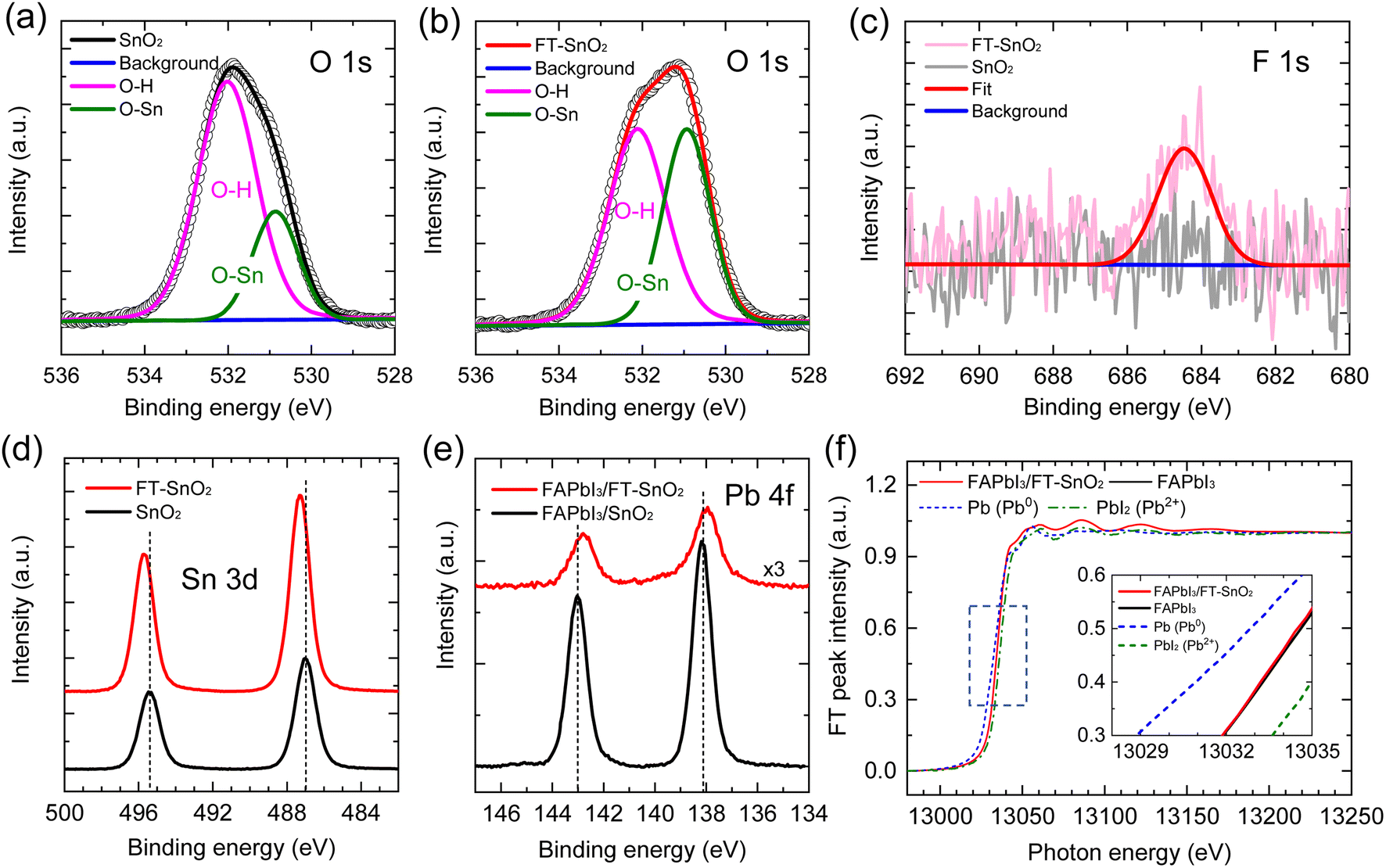 | ||
| Fig. 1 O 1s XPS data for (a) bare SnO2 and (b) SnO2 modified with 4-fluorothiophenol (FT-SnO2). (c) F 1s and (d) Sn 3d XPS spectra of bare SnO2 and FT-SnO2. (e) Pb 4f XPS spectra and (f) Pb L3 edge XANES spectra of FAPbI3 black powder and FAPbI3-coated FT-SnO2 powder. XANES spectra of metal Pb and PbI2 were measured for reference. Inset shows XANES data of the rectangular dashed line region. | ||
The effect of halogen-substituted thiophenol (4-bromothiophenol, 4-chlorothiophenol and 4-fluorothiophenol) on photovoltaic performance was investigated. As compared to the PCE of a device based on bare SnO2, post-treated SnO2-based devices show higher PCEs (Fig. S4†). It is noted that photovoltaic performance is likely to depend on halogen, where PCE becomes lower in the following order: FT-SnO2 > BrT-SnO2 > ClT-SnO2, where BrT-SnO2 and ClT-SnO2 represent 4-bromothiophenol-treated SnO2 and 4-chlorothiophenol-treated SnO2, respectively. Comparative study between thiophenol without halogen substituent and 4-fluorothiophenol in Fig. S5† reveals higher performance for FT-SnO2 than thiophenol-treated SnO2 (T-SnO2). Since FT-SnO2 showed better photovoltaic performance than the other two candidates of BrT-SnO2 and ClT-SnO2, further studies were carried out with FT-SnO2 and compared with bare SnO2.
Fig. 2(a) compares current density–voltage (J–V) curves of best performing n-i-p type PSCs before and after surface treatment with 5 mM 4-fluorothiophenol, where optimal concentration is determined from the study of the effect of 4-fluorothiophenol concentration on photovoltaic parameters (Fig. S6†). PCE averaged out from reverse and forward scanned data is enhanced from 21.15% to 22.96% as a result of the surface treatment due to a significant increase in fill factor (FF) along with a slight increase in both photocurrent density (Jsc) and Voc. The relevant photovoltaic parameters are listed in Table 1. External quantum efficiency (EQE) in Fig. 2(b) shows a slight increase in the wavelength ranging from 350 nm to 400 nm for FT-SnO2, which is indicative of an improved charge collection efficiency due to the surface modification at the electron collecting layer in the n-i-p structure.33 Statistical photovoltaic parameters are shown in Fig. 2(c–f). Bare SnO2-based PSCs show mean Jsc of 24.998 ± 0.248 mA cm−2, Voc of 1.1189 ± 0.0144 V and FF of 75.22 ± 2.40%, leading to a mean PCE of 20.88 ± 0.80%, whereas FT-SnO2-based ones demonstrate an improved mean PCE of 22.82 ± 0.58% due to the enhanced mean Jsc of 25.231 ± 0.400 mA cm−2, Voc of 1.1336 ± 0.0061 V and FF of 80.25 ± 2.58%. Stabilized power output (SPO) at maximum power point shows that 89.1% of SPO (20.2%) was maintained after 2000 s for the bare SnO2, whereas the FT-SnO2-based device demonstrates more stable PCE of 94.4% of SPO (21.5%) after 2000 s (Fig. S7†). A substantial increase in FF is in part ascribed to the increased conductivity of SnO2 after 4-fluorothiophenol modification (Fig. S8†). The degree of enhancement in photovoltaic performance after surface treatment of the CBD-based SnO2 in this work is compared with those reported elsewhere (Table S2†), where a slight enhancement from 22.4% to 23.2% and 19.69% to 21.24% was observed due to the slightly enhanced Voc and/or FF without alteration of Jsc (relevant references are in the ESI†). This tendency is consistent with what we observed in this work. For the case of spin-coated SnO2 in Table S2†, Jsc seems to be enhanced after surface treatment of SnO2 due to the enhanced surface coverage resulting from surface treatment.
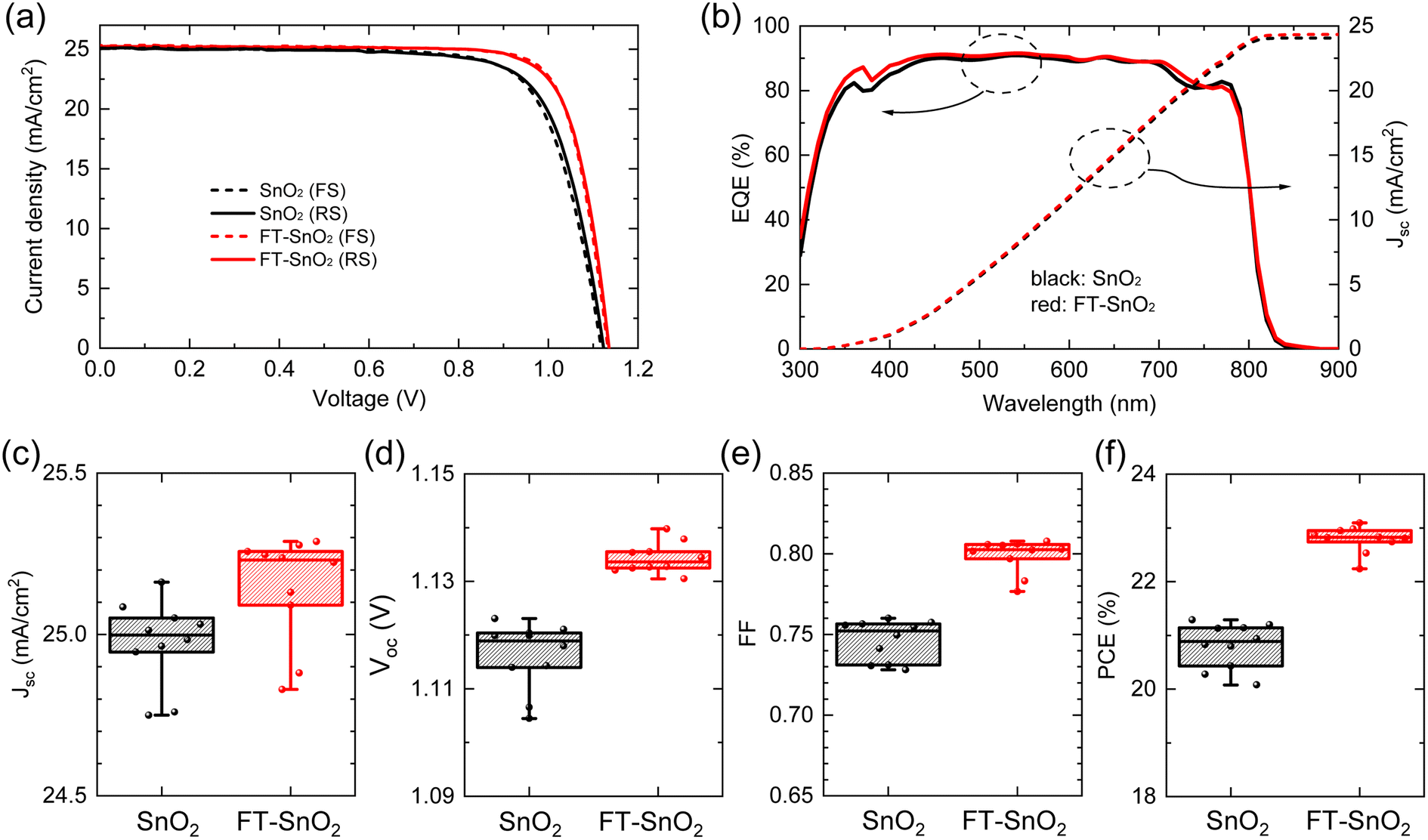 | ||
| Fig. 2 (a) J–V curves of the best performing PSCs based on bare SnO2 and FT-SnO2. Solid and dashed lines represent reverse scan (RS) and forward scan (FS), respectively. (b) EQE and integrated Jsc of the best performing PSCs based on bare SnO2 and FT-SnO2. Statistical photovoltaic parameters of (c) Jsc, (d) Voc, (e) FF and (f) PCE for PSCs based on bare SnO2 and FT-SnO2. Data were collected under 1 sun illumination with devices having an aperture area of 0.125 cm2. | ||
| ETL | Scan direction | J sc (mA cm−2) | V oc (V) | FF (%) | PCE (%) |
|---|---|---|---|---|---|
| SnO2 | Reverse | 25.085 | 1.1231 | 75.58 | 21.29 |
| SnO2 | Forward | 25.032 | 1.1180 | 75.75 | 21.20 |
| FT-SnO2 | Reverse | 25.223 | 1.1355 | 79.70 | 22.83 |
| FT-SnO2 | Forward | 25.288 | 1.1327 | 80.60 | 23.09 |
SEM images show that surface morphology of the perovskite layer does not seem to be affected by the surface modification. However, perovskite grains are increased to ∼1000 nm upon deposition on the FT-SnO2 layer as compared to the mean size of ∼850 nm grown on the bare SnO2 layer (Fig. 3(a and b)). X-ray diffraction (XRD) data show little change in crystal structure of the perovskite film before and after surface modification of SnO2 (Fig. 3(c)), which might be related to the surface roughness22 being unaffected by the passivation (Table S3†). In addition, absorption onset and absorbance of the perovskite films are also unaffected by the surface modification (Fig. 3(d)). Optical transmittance (Fig. S9†) and morphological and topographical properties (Fig. S10†) of SnO2 are hardly changed by the surface passivation, which seems to be responsible for little change in both absorbance and morphology of perovskite. Thus, the increased Jsc might be related an improved charge collection efficiency and/or charge extraction capability.
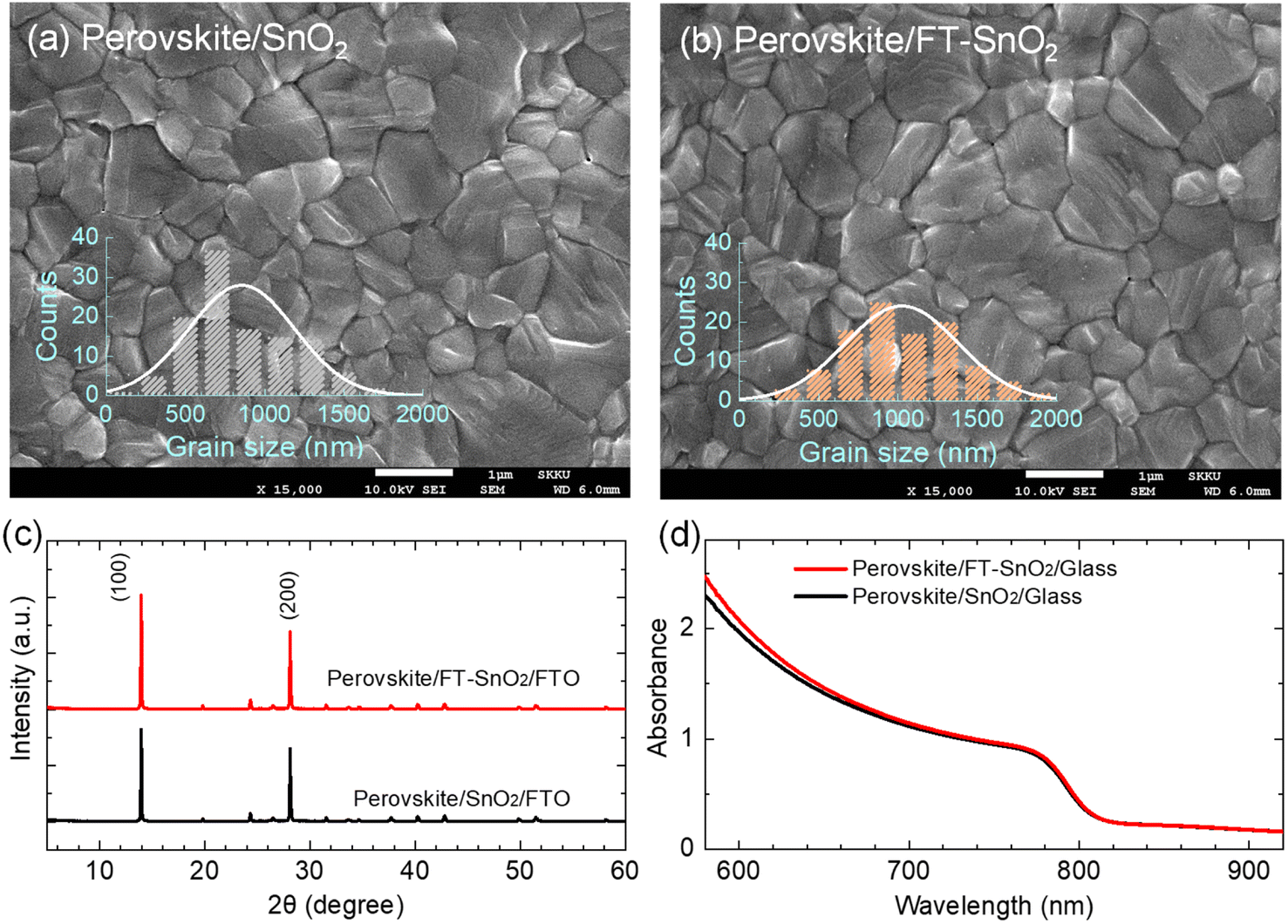 | ||
| Fig. 3 Top-view SEM image of the perovskite layer coated on (a) bare SnO2 and (b) FT-SnO2. Insets show grain size distribution. (c) XRD patterns of the perovskite films formed on SnO2- and FT-SnO2-coated FTO substrate. (d) Absorbance of the perovskite films deposited on SnO2- and FT-SnO2-coated glass substrate. | ||
To understand the effect of surface passivation of the SnO2 layer on electron extraction and carrier lifetime of the perovskite layer, steady-state photoluminescence (SSPL) and time-resolved photoluminescence (TRPL) were investigated. SSPL in Fig. 4(a) shows that PL is quenched more effectively for FT-SnO2 than for bare SnO2, which indicates that electron transfer from perovskite to SnO2 is improved by the surface modification. Decay in PL intensity of TRPL data in Fig. 4(b) is fitted using a biexponential decay equation, 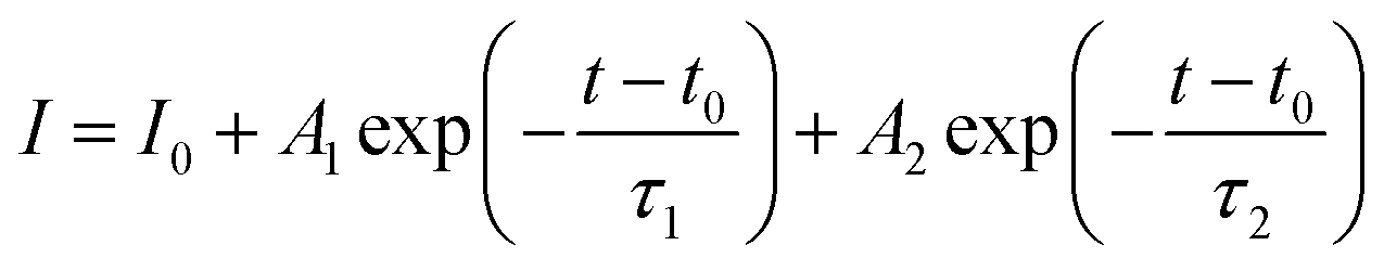 , where the fast decay time (τ1) and the slow decay time (τ2) are related to the charge extraction by ETL and radiative recombination in bulk perovskite film, respectively.5,34–36 Average life time (τavg) is calculated using the equation
  . Parameters obtained by fitting TRPL data are listed in Table 2, where τ1 and τ2 decrease from 5.7 ns to 5.0 ns and from 70 ns to 48 ns, respectively, after surface modification. As a result, τavg decreases from 64.6 ns to 43.1 ns, which indicates that electron transfer is kinetically favorable for FT-SnO2. Space-charge-limited current (SCLC) was measured with an electron-only device of FTO/SnO2 (or FT-SnO2)/perovskite/PCBM/BCP/Au to investigate defect density, where dark current–voltage curves in Fig. 4(c) and (d) are analyzed as follows. There are three typical regions depending on bias voltage: ohmic at low voltage, trap-filled-limited at medium voltage and child region at high voltage. The trap-filled-limited voltage (VTFL) is estimated by the relation VTFL = qntL2/2ε0ε, where L, q, nt, ε0 and ε are the thickness of the perovskite (580 nm in this study), the electric charge (1.602 × 10⁻¹⁹ C), the trap density, the vacuum permittivity (8.8542 × 10⁻¹⁴ F cm−1) and the dielectric constant of perovskite, respectively.37ε is calculated using the geometrical capacitance at 1.0608 × 10⁴ Hz obtained from capacitance–frequency plots (Fig. S11†).29 All parameters are listed in Table S4†. It is found that nt decreases from 6.42 × 1015 cm−3 to 4.95 × 1015 cm−3 due to the fact that VTFL is lowered from 0.563 V to 0.407 V as a result of the surface passivation of SnO2 with 4-fluorothiophenol. Since surface passivation of SnO2 decreases the defects of the perovskite film, defects are assumed to be concentrated at the SnO2/perovskite interface. In addition, electrochemical impedance spectroscopy (EIS) was used to understand transfer resistance. Fig. 4(e) shows Nyquist plots measured at a bias voltage of 0.8 V under illumination, which were fitted with an equivalent circuit having series resistance (Rs), charge transfer resistance (Rct) and constant phase element (CPE), which are listed in Table S5†. Rct is decreased from 151.5 Ω to 139.4 Ω upon surface passivation of SnO2, which implies that FT-SnO2 is more beneficial for electron extraction than bare SnO2.9 TRPL, SCLC and EIS studies explain well the basis for the increased Voc and FF as well as Jsc.
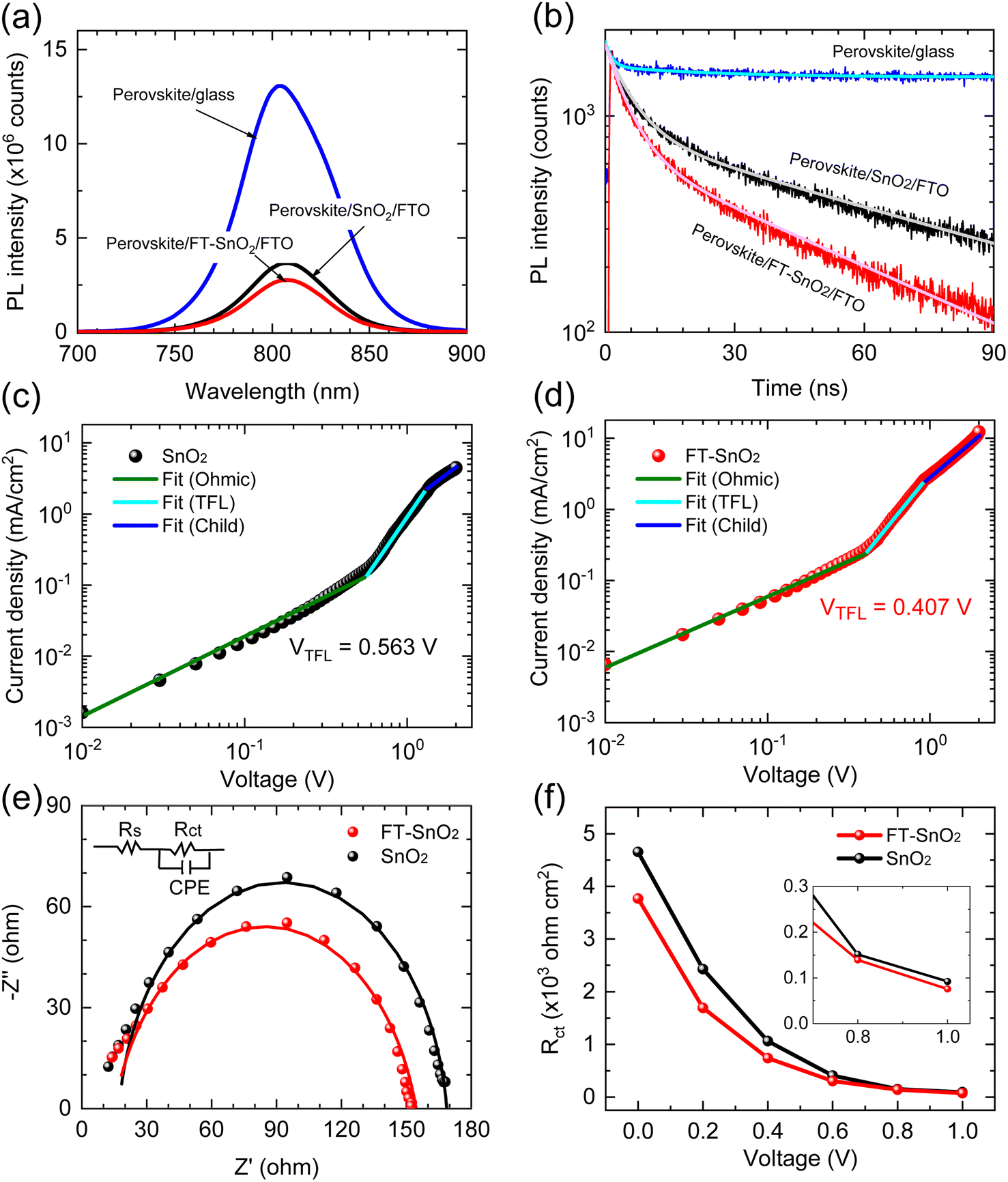 | ||
| Fig. 4 (a) SSPL and (b) TRPL of perovskite films deposited on SnO2- and FT-SnO2-coated FTO substrate. Perovskite film formed on a plane glass substrate was also measured as reference. Dark current density–voltage curves of electron-only devices: (c) FTO/SnO2/perovskite/PCBM/BCP/Au and (d) FTO/FT-SnO2/perovskite/PCBM/BCP/Au. The different regions were fitted to obtain VTFL. (e) Nyquist plots of PSCs based on SnO2 and FT-SnO2 measured at a bias voltage of 0.8 V under one sun illumination. Inset shows an equivalent circuit to fit the data. (f) Rct as a function of applied voltage extracted from the Nyquist plots. Inset shows Rct at high voltage bias region. | ||
| Sample | τ 1 (ns) | A 1 (%) | τ 2 (ns) | A 2 (%) | τ avg (ns) |
|---|---|---|---|---|---|
| SnO2 | 5.7 | 52.94 | 70 | 47.06 | 64.6 |
| FT-SnO2 | 5.0 | 55.17 | 48 | 44.83 | 43.1 |
Long-term stability was investigated to determine any positive effect from the FT-SnO2. Fig. 5(a) compares PCE of PSC based on FT-SnO2 with that based on bare SnO2, where the devices were stored for 500 h at ambient condition without encapsulation. The perovskite deposited on bare SnO2 shows a quick degradation leading to 59.7% of initial PCE after 500 h; on the other hand, the perovskite formed on FT-SnO2 maintains 90% of initial PCE after 500 h. This superior stability observed by surface passivation of SnO2 with 4-fluorothiophenol underlines that the interface between SnO2 and perovskite is critical in degradation. The cross-sectional SEM images of the 500 h-aged PSCs are compared. As compared to the PSC based on FT-SnO2 in Fig. 5(c), pinholes are generated at the interface for the perovskite film deposited on bare SnO2 (Fig. 5(b)). Pinholes are formed at specific sites, not at all the interfaces, which indicates that there are sites for creating pinholes. However, it cannot be ruled out that some of pinholes might exist before aging in the bare SnO2/perovskite interface because pinholes can be induced by unwetted perovskite on bare SnO2. We confirm that no pinholes are detected for both SnO2 and FT-SnO2 (Fig. S12†). Thus, pinholes after aging result from degradation. It was reported that hydroxyl defects on SnO2 surface could deprotonate methylammonium ion (MA+) and thereby pinholes were generated in the vicinity of the perovskite/SnO2 interface.38–40 Therefore, no pinholes generated for the perovskite film deposited on the FT-SnO2 is attributed to the effective passivation of hydroxyl defects by 4-fluorothiophenol.
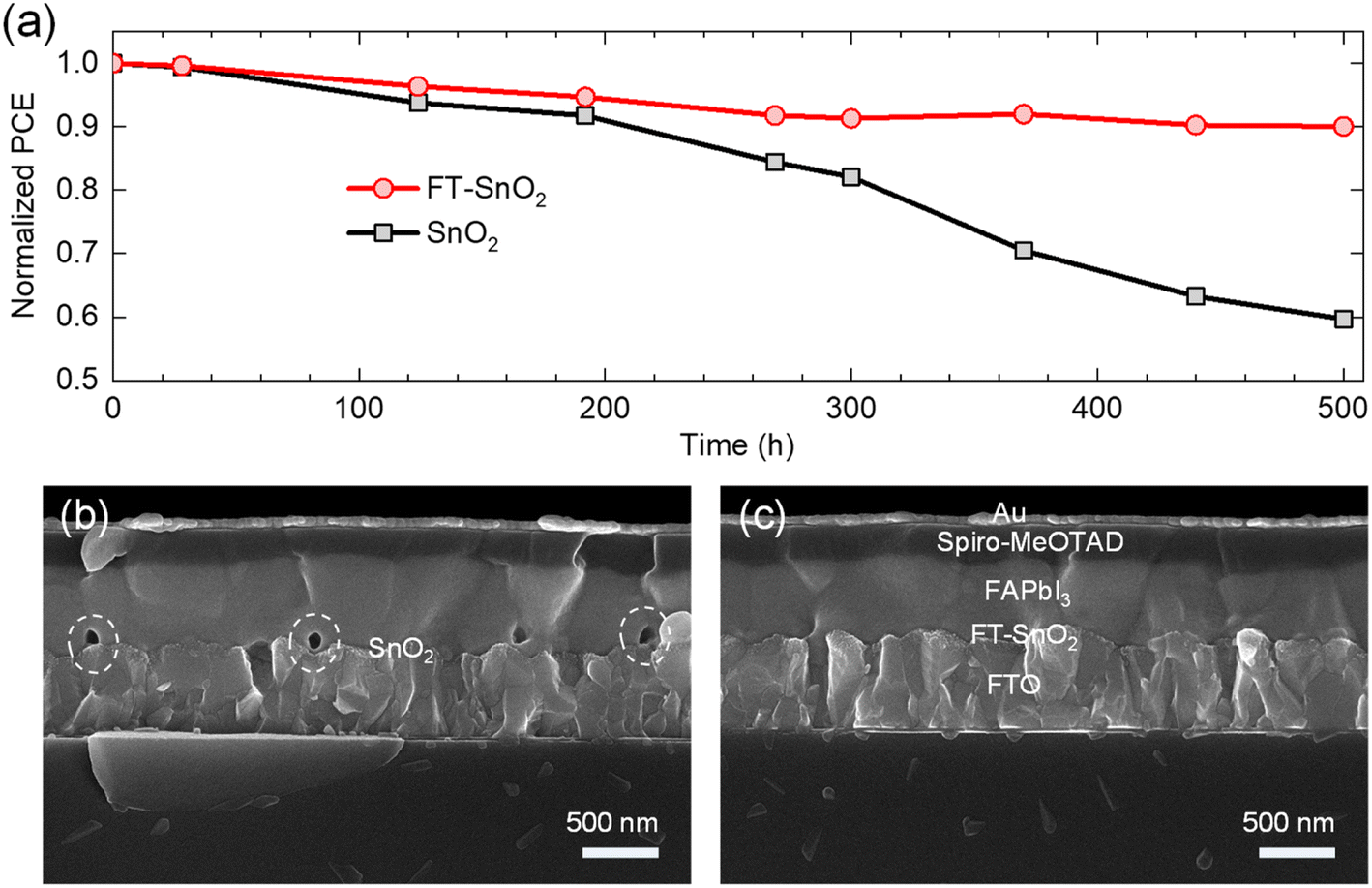 | ||
| Fig. 5 (a) Comparison of normalized PCE of PSCs based on bare SnO2 and FT-SnO2. The devices were stored in the dark at room temperature and under relative humidity of 25 ± 10% for 500 h. Cross-sectional SEM images of the 500 h-aged PSCs based on (b) bare SnO2 and (c) FT-SnO2. | ||
3. Conclusions
In this work, we have studied the effect of passivation of SnO2 surface defects on photovoltaic performance and stability of PSCs. Post-treatment of the annealed SnO2 film with 4-fluorothiophenol reduced the density of hydroxyl groups on the SnO2 surface, which eventually improved the stability of PSCs. Bare SnO2 with more hydroxyl groups produced pinholes near the interface between perovskite and SnO2, which was responsible for degradation. On the other hand, no pinholes were found for the perovskite deposited on FT-SnO2 due to the substantial reduction of hydroxyl groups. Furthermore, surface passivation with 4-fluorothiophenol improved electron extraction from perovskite to SnO2 and carrier lifetime of the perovskite layer, which led to an improvement of Jsc, Voc and FF. We demonstrated a PCE over 23% together with stability maintaining 90% of initial PCE after 500 h. A negative influence of hydroxyl groups on the SnO2 surface was found from this work and passivation of hydroxyl groups with halogen-substituted thiophenol was one effective way to improve stability and efficiency of PSCs.4. Experimental
4.1. Material synthesis
Formamidinium iodide (FAI) powder was synthesized by reacting 30 mL of HI (57 wt% in H2O, Sigma-Aldrich) and 15 g of formamidinium acetate (99%, Sigma-Aldrich) in an ice bath for 1 h with stirring. The precipitates were collected by using a rotary evaporator at 65 °C. The collected FAI powder was purified by dissolving in ethanol and then adding diethyl ether (99%, SAMCHUN), which was dried in a vacuum chamber for 48 h.Formamidinium lead triiodide (FAPbI3) black powder was synthesized by mixing 1.6 M as-synthesized FAI and PbI2 (99.99%, TCI) in γ-butyrolactone (GBL, 99.5%, SAMCHUN) and heating at 130 °C for 2 h under vigorous stirring. The black powder was washed with acetonitrile (ACN, 99.9%, SAMCHUN) and diethyl ether several times, which was followed by drying at 150 °C for 30 min.
Methylammonium lead tribromide (MAPbBr3) single crystals were synthesized by mixing 1.4 M methylammonium bromide (MABr, 99.99%, Greatcellsolar) and PbBr2 (98%, TCI) in dimethylformamide (DMF, 99.8%, Sigma-Aldrich), where the solution was heated at 110 °C for 2 h. To remove unreacted chemicals, the single crystals were washed with ACN and diethyl ether several times, which were then dried at 100 °C for 30 min.
4.2. Device fabrication
Fluorine-doped tin oxide (FTO) glass (Asahi) was cleaned by successive sonication in detergent, deionized water, acetone and ethanol for 15 min. Prior to deposition of SnO2, UV-ozone (UVO) treatment was performed on the cleaned FTO substrates for 30 min. For CBD to prepare SnO2 film, the coating solution was prepared by mixing 137.5 mg of SnCl2·2H2O (99.99%, Sigma-Aldrich), 625 mg of urea (99%, Sigma-Aldrich), 625 μL of HCl (37 wt%, Sigma-Aldrich), 12.5 μL of thioglycolic acid (99%, Sigma-Aldrich) and 50 mL of deionized water, in which the cleaned FTO was dipped at 90 °C for 4 h. After CBD, the SnO2-coated FTO substrate was washed with deionized water and isopropanol for 10 min using sonication, which was followed by heating at 185 °C for 30 min. For the post-treatment of the SnO2 layer, a 5 mM ethanol solution of 4-fluorothiophenol was spin-coated at 3000 rpm for 20 s, which was followed by annealing at 150 °C for 10 min. Perovskite precursor solution was prepared by mixing 844 mg of the as-made FAPbI3 powder, 6.4 mg of MAPbBr3 single crystals, 17.9 mg of MACl (99.99%, Greatcellsolar), 718.5 μL of DMF, 99.1 μL of dimethyl sulfoxide (DMSO, 99.9%, Sigma-Aldrich), 25 μL of KI (99.99%, Sigma-Aldrich) stock solution (8.85 mg of KI was dissolved in 1 mL of DMF). The perovskite precursor solution was spin-coated on the SnO2-coated FTO substrate at 1000 rpm for 5 s and then 5000 rpm for 20 s, where 1000 μL of diethyl ether (99.9%, Sigma-Aldrich) was dropped on the rotating substrate at 5 s before ending the spinning program. The as-deposited perovskite film was annealed at 150 °C for 10 min. After cooling down the substrate, spiro-MeOTAD (2,2′,7,7′-tetrakis[N,N-di(4-methoxyphenyl)amino]-9,9′-spirobifluorene) was spin-coated at 3000 rpm for 20 s using 20 μL of the solution. The spiro-MeOTAD coating solution was prepared by dissolving 90 mg of spiro-MeOTAD, 39.5 μL of 4-tert-butylpyridine (tBP, 98%, Sigma-Aldrich), 23 μL of bis(trifluoromethane)sulfonimide lithium salt (LiTFSI, 99.95%, Sigma-Aldrich) stock solution (520 mg of LiTFSI was dissolved in 1 mL of ACN) and 10 μL of bis(trifluoromethylsulfonyl)imide cobalt(III) salt (Co(TFSI)3, 99%, Lumtec) stock solution (375 mg of Co(TFSI)3 was dissolved in 1 mL of ACN) in 1 mL of chlorobenzene (99.8%, Sigma-Aldrich). Finally, an 80 nm-thick Au electrode was deposited by thermal evaporation.4.3. Optoelectronic and photovoltaic characterizations
Current density–voltage (J–V) curves were measured using a Keithley 2400 source meter under AM 1.5 G one sun illumination (100 mW cm−2) generated by a solar simulator (Oriel Sol 3A class AAA) equipped with a 450 W xenon lamp (Newport 6280 NS). The one sun intensity was adjusted by a NREL calibrated Si solar cell with a KG-2 filter. The device was covered with an aperture metal mask with area of 0.125 cm2 during measurement. All J–V curves were measured at scan rate of 130 mV s−1. XRD data were obtained using a Rigaku Smart Lab diffractometer with Cu Kα radiation (λ = 1.5406 Å) at a scan rate of 4° min−1 and step size of 0.02°. Optical absorption was measured using a UV-visible spectrometer (Lambda 45, PerkinElmer). SEM (JSM-7600F, JSM-IT800, JEOL) images were obtained to investigate cross-sectional PSCs. Elemental distribution on the surface of SnO2 was observed by EDS using SEM. EQE spectra were collected by using an QEX-7 series system (PV Measurements Inc.) in which a monochromatic beam was generated by a 75 W xenon source lamp (USHIO, Japan) under DC mode. SSPL was measured using a fluorescence spectrometer (Quantaurus Tau C11367-12, Hamamatsu). Perovskite films were photoexcited with a 464 nm laser pulsed at a frequency of 10 MHz and then the emitted PL was collected by a photomultiplier tube (PMT) detector (PMA 182, Pico Quant-GmbH) at 805 nm. For TRPL measurement, a repetition frequency of 2 MHz was used. XPS was carried out with an ESCALAB250 instrument (Thermo Fisher Scientific) by using a monochromatized Al source (hν = 1486.6 eV). Binding energy was calibrated with respect to C 1s peak of 284.6 eV. UPS was conducted by using an ESCALAB 250 instrument (Thermo Fisher Scientific) with He I (21.22 eV). XANES measurements were conducted at the PLS-II 10C PAL beamline of Pohang Accelerator Laboratory (PAL). With an X-ray incident angle of 0.5°, the data were collected with fluorescence mode. The XANES spectra were calibrated as the first derivative of X-ray absorption coefficient (μ(E)) for the L3-edge energy of Pb foil (13![[thin space (1/6-em)]](https://www.rsc.org/images/entities/char_2009.gif) 035 eV) measured simultaneously with the sample. For background reduction, the pre-edge condition and normalization condition were set from −150 eV to −45 eV and 150 eV to 871.7 eV, respectively. All the data fitting processes were conducted through ATHENA.41 EIS measurement data were obtained from an Autolab electrochemical working station with an amplitude of 20 mV at voltage ranging from 0.0 V to 1.0 V under one sun illumination. The frequency range was 1 MHz to 850 Hz.
035 eV) measured simultaneously with the sample. For background reduction, the pre-edge condition and normalization condition were set from −150 eV to −45 eV and 150 eV to 871.7 eV, respectively. All the data fitting processes were conducted through ATHENA.41 EIS measurement data were obtained from an Autolab electrochemical working station with an amplitude of 20 mV at voltage ranging from 0.0 V to 1.0 V under one sun illumination. The frequency range was 1 MHz to 850 Hz.
Author contributions
N.-G. P. conceived and supervised the research direction. Y.-S. J. conducted experiments and measurements. J.-H. K. assisted in analyzing SCLC and impedance data. D.-H. K. measured and analyzed XANES. Y.-S. J. wrote the draft. N.-G. P. edited the manuscript. All authors discussed the results and revised the manuscript.Conflicts of interest
There is no conflict to declare.Acknowledgements
This work was supported by National Research Foundation of Korea (NRF) grants funded by the Korean government (MSIT) under Contract NRF-2021R1A3B1076723 (Research Leader Program) and NRF-2022M3J1A1085280 (Carbon Neutral Technology Program). Authors thank D.-K. Lee for discussion on the preparation of XPS samples.References
- H.-S. Kim, C.-R. Lee, J.-H. Im, K.-B. Lee, T. Moehl, A. Marchioro, S.-J. Moon, R. Humphry-Baker, J.-H. Yum and J. E. Moser, Sci. Rep., 2012, 2, 1–7 Search PubMed.
- NREL's “Best Research-Cell Efficiency Chart”, https://www.nrel.gov/pv/assets/pdfs/best-research-cell-efficiencies-rev220630.pdf, accessed 30 October, 2022 Search PubMed.
- M. Faizan, X. Wang, S. A. Abdelmohsen, K. Bhamu, S. Sappati, A. Laref, N. Muhammad, M. Mushtaq, A. M. Abdelbacki and R. Khenata, Energy Fuels, 2022, 36, 7065–7074 CrossRef CAS.
- J. Y. Kim, J.-W. Lee, H. S. Jung, H. Shin and N.-G. Park, Chem. Rev., 2020, 120, 7867–7918 CrossRef CAS PubMed.
- S.-H. Lee, S. Jeong, S. Seo, H. Shin, C. Ma and N.-G. Park, ACS Energy Lett., 2021, 6, 1612–1621 CrossRef CAS.
- M. Kim, G.-H. Kim, T. K. Lee, I. W. Choi, H. W. Choi, Y. Jo, Y. J. Yoon, J. W. Kim, J. Lee and D. Huh, Joule, 2019, 3, 2179–2192 CrossRef CAS.
- H. Min, D. Y. Lee, J. Kim, G. Kim, K. S. Lee, J. Kim, M. J. Paik, Y. K. Kim, K. S. Kim and M. G. Kim, Nature, 2021, 598, 444–450 CrossRef CAS PubMed.
- J. J. Yoo, G. Seo, M. R. Chua, T. G. Park, Y. Lu, F. Rotermund, Y.-K. Kim, C. S. Moon, N. J. Jeon and J.-P. Correa-Baena, Nature, 2021, 590, 587–593 CrossRef CAS PubMed.
- D. Yang, R. Yang, K. Wang, C. Wu, X. Zhu, J. Feng, X. Ren, G. Fang, S. Priya and S. F. Liu, Nat. Commun., 2018, 9, 1–11 CrossRef.
- D. Bi, C. Yi, J. Luo, J.-D. Décoppet, F. Zhang, S. M. Zakeeruddin, X. Li, A. Hagfeldt and M. Grätzel, Nat. Energy, 2016, 1, 1–5 Search PubMed.
- K. G. Godinho, A. Walsh and G. W. Watson, J. Phys. Chem. C, 2009, 113, 439–448 CrossRef CAS.
- T. Cao, K. Chen, Q. Chen, Y. Zhou, N. Chen and Y. Li, ACS Appl. Mater. Interfaces, 2019, 11, 33825–33834 CrossRef CAS PubMed.
- G. Tong, L. K. Ono, Y. Liu, H. Zhang, T. Bu and Y. Qi, Nano-Micro Lett., 2021, 13, 1–14 Search PubMed.
- E. H. Jung, B. Chen, K. Bertens, M. Vafaie, S. Teale, A. Proppe, Y. Hou, T. Zhu, C. Zheng and E. H. Sargent, ACS Energy Lett., 2020, 5, 2796–2801 CrossRef CAS.
- A. A. Peterson and J. K. Nørskov, J. Phys. Chem. Lett., 2012, 3, 251–258 CrossRef CAS.
- G. Qu, D. Khan, F. Yan, A. Atsay, H. Xiao, Q. Chen, H. Xu, I. Nar and Z.-X. Xu, J. Energy Chem., 2022, 67, 263–275 CrossRef CAS.
- K. Choi, J. Lee, H. I. Kim, C. W. Park, G.-W. Kim, H. Choi, S. Park, S. A. Park and T. Park, Energy Environ. Sci., 2018, 11, 3238–3247 RSC.
- L. Zuo, Q. Chen, N. De Marco, Y.-T. Hsieh, H. Chen, P. Sun, S.-Y. Chang, H. Zhao, S. Dong and Y. Yang, Nano Lett., 2017, 17, 269–275 CrossRef CAS.
- G. Tumen-Ulzii, T. Matsushima, D. Klotz, M. R. Leyden, P. Wang, C. Qin, J.-W. Lee, S.-J. Lee, Y. Yang and C. Adachi, Commun. Mater., 2020, 1, 1–7 CrossRef.
- S. Ullah, M. F. U. Din, J. Khan Kasi, A. Khan Kasi, K. Vegso, M. Kotlar, M. Micusik, M. Jergel, V. Nadazdy and P. Siffalovic, ACS Appl. Nano Mater., 2022, 5, 7822–7830 CrossRef CAS.
- S. Sonmezoglu and S. Akin, Nano Energy, 2020, 76, 105127 CrossRef CAS.
- N. Guan, C. Ran, Y. Wang, L. Chao, Z. Deng, G. Wu, H. Dong, Y. Bao, Z. Lin and L. Song, ACS Appl. Mater. Interfaces, 2022, 14, 34198–34207 CrossRef CAS PubMed.
- E. Jiang, Y. Ai, J. Yan, N. Li, L. Lin, Z. Wang, C. Shou, B. Yan, Y. Zeng, J. Sheng and J. Ye, ACS Appl. Mater. Interfaces, 2019, 11, 36727–36734 CrossRef CAS PubMed.
- Z. Dai, S. K. Yadavalli, M. Chen, A. Abbaspourtamijani, Y. Qi and N. P. Padture, Science, 2021, 372, 618–622 CrossRef CAS PubMed.
- J. Yan, Z. Lin, Q. Cai, X. Wen and C. Mu, ACS Appl. Energy Mater., 2020, 3, 3504–3511 CrossRef CAS.
- Y. Luan, X. Yi, P. Mao, Y. Wei, J. Zhuang, N. Chen, T. Lin, C. Li and J. Wang, iScience, 2019, 16, 433–441 CrossRef CAS PubMed.
- A. Rizzato, C. V. Santilli, S. H. Pulcinelli, Y. Messaddeq and P. Hammer, J. Sol-Gel Sci. Technol., 2004, 32, 155–160 CrossRef CAS.
- J. Chen, X. Zhao, S. G. Kim and N. G. Park, Adv. Mater., 2019, 31, 1902902 CrossRef PubMed.
- D.-H. Kang, C. Ma and N.-G. Park, ACS Appl. Mater. Interfaces, 2022, 14, 8984–8991 CrossRef CAS PubMed.
- P. J. Hotchkiss, H. Li, P. B. Paramonov, S. A. Paniagua, S. C. Jones, N. R. Armstrong, J. L. Brédas and S. R. Marder, Adv. Mater., 2009, 21, 4496–4501 CrossRef CAS.
- P. K. Santra, A. F. Palmstrom, J. T. Tanskanen, N. Yang and S. F. Bent, J. Phys. Chem. C, 2015, 119, 2996–3005 CrossRef CAS.
- V.-H. Tran, S.-K. Kim and S.-H. Lee, ACS Omega, 2019, 4, 19225–19237 CrossRef CAS PubMed.
- J.-H. Im, H.-S. Kim and N.-G. Park, APL Mater., 2014, 2, 081510 CrossRef.
- J.-W. Lee, S.-H. Bae, Y.-T. Hsieh, N. De Marco, M. Wang, P. Sun and Y. Yang, Chem, 2017, 3, 290–302 CAS.
- H. Zhou, Q. Chen, G. Li, S. Luo, T.-b. Song, H.-S. Duan, Z. Hong, J. You, Y. Liu and Y. Yang, Science, 2014, 345, 542–546 CrossRef CAS.
- D. W. de Quilettes, S. M. Vorpahl, S. D. Stranks, H. Nagaoka, G. E. Eperon, M. E. Ziffer, H. J. Snaith and D. S. Ginger, Science, 2015, 348, 683–686 CrossRef CAS PubMed.
- J. Chen and N.-G. Park, ACS Energy Lett., 2020, 5, 2742–2786 CrossRef CAS.
- S. Y. Park and K. Zhu, Adv. Mater., 2022, 34, 2110438 CrossRef CAS PubMed.
- Z. Liu, L. Qiu, L. K. Ono, S. He, Z. Hu, M. Jiang, G. Tong, Z. Wu, Y. Jiang and D.-Y. Son, Nat. Energy, 2020, 5, 596–604 CrossRef CAS.
- L. Zhang and P. H.-L. Sit, J. Phys. Chem. C, 2015, 119, 22370–22378 CrossRef CAS.
- D.-H. Kang, Y.-J. Park, Y.-S. Jeon and N.-G. Park, J. Energy Chem., 2022, 67, 549–554 CrossRef CAS.
Footnote |
| † Electronic supplementary information (ESI) available. See DOI: https://doi.org/10.1039/d2ta08488k |
| This journal is © The Royal Society of Chemistry 2023 |