
 Open Access Article
 This Open Access Article is licensed under a Creative Commons Attribution-Non Commercial 3.0 Unported Licence
Suppression of the redox reaction between the IGZO surface and the reducing agent TMA using fluorine oxidizing agent treatment†
Yuseong Jang ,
Jinkyu Lee,
Jinsung Mok,
Junhyeong Park,
Seung Yoon Shin and
Soo-Yeon Lee*
,
Jinkyu Lee,
Jinsung Mok,
Junhyeong Park,
Seung Yoon Shin and
Soo-Yeon Lee*
Department of Electrical and Computer Engineering, Inter-University Semiconductor Research Center, Seoul National University, 1 Gwanak-ro, Gwanak-gu, Seoul, 08826, Republic of Korea. E-mail: sooyeon.lee@snu.ac.kr
First published on 13th November 2023
Abstract
We propose that the post-deposition oxidation of the IGZO surface is essential for improving the interface quality, with Al2O3 prepared by atomic layer deposition (ALD) employing a common metal precursor trimethylaluminum (TMA). Here, the ALD-Al2O3 process was conducted using H2O as an oxidant at a substrate temperature of 150 °C after IGZO deposition. The depth-resolved X-ray photoelectron spectroscopy (XPS) and transmission electron microscopy (TEM) data reveal the defect-rich and poor interface of the standard Al2O3/IGZO stack due to the redox reaction between the IGZO surface and TMA. The anion character of the IGZO was modified by introducing fluorine, which is known as a stability enhancer for oxide semiconductors. We highlight that the presence of the fluorine also improves the interface quality with ALD-Al2O3. As a consequence of the fluorine incorporation prior to the ALD-Al2O3 process, the chemical reduction reaction of the IGZO surface was effectively alleviated, resulting in a defect-passivated and sharp interface owing to the strong oxidizing nature of the fluorine.
Introduction
CMOS (complementary metal-oxide semiconductor) compatibility, wide optical bandgap (>3.0 eV), and low-temperature processes have been driving InGaZnO (IGZO) thin-film transistors (TFTs) toward future electronic devices.1–3 In particular, the low off-current of IGZO has attracted intensive efforts in both academia and industry for capacitor-less DRAM (dynamic random access memory) technology.4–8 Undoubtedly, in the regulation of native defects of oxide semiconductors, oxygen vacancies (VOs), have been the most important topic. In general, many studies have attempted to passivate the VO by either cation or anion engineering. Cation doping, such as with Hf, can reduce the VO concentration because of the strong metal–oxygen (M–O) bond strength.9 It should be noted that the conduction band composed of large spherical s orbitals can be influenced depending on the cation dopant species. In terms of anion modification, the VO states can be occupied by N, which has a higher orbital energy and larger ionic radius than O.10 However, the metastability of metal nitride thin films remains to be addressed,11 even though the M–N bond can be even stronger than the M–O bond based on thermodynamic calculations.12 On the other hand, F is another promising element because the smaller atomic radius and stronger electronegativity than O lead to VO passivation and strong M–F bond formation.13,14 Therefore, TFT stability is enhanced when F is incorporated into IGZO.15–17 Furthermore, the presence of F reduces the vulnerability of IGZO to H penetration from plasma enhanced chemical vapor deposited (PECVD)-SiO2.18 The type and concentration of H species from the adjacent insulator are another major issue in discussing the device performance of IGZO TFT.19 Therefore, attention should be paid to the gate insulator (GI) material, preparation, and process sequence. Atomic layer deposited Al2O3 (ALD-Al2O3) benefits from excellent step coverage, a low-temperature process, high-k, and large band offset with IGZO. In this regard, ALD-Al2O3 on IGZO (hereafter, ALD-Al2O3/IGZO stack) has been widely utilized in TFT configurations, where the Al2O3 functions as a top GI,5,20–22 passivation layer,23 and other functional layers.24,25 However, there are several phenomena that should be addressed behind the ALD-Al2O3/IGZO stack. At the low substrate temperature of the ALD process, a large H concentration can be derived as a result of the incomplete combustion of hydroxyl groups,26 so H diffusion into the underlying IGZO would be unavoidable. Moreover, the chemical reaction of the IGZO surface occurs during ALD-Al2O3, attributed to a common Al precursor, trimethylaluminum (TMA).20 TMA is known to be a strong reducing agent,27–29 which itself desires to be oxidized. The capability of TMA to reduce neighboring species has been the main cause of defect-rich interfaces, forming a two-dimensional electron gas (2DEG) between ALD-Al2O3 and bottom binary oxides such as TiO2,28,29 ZnO,27,30 and In2O3.31,32 Likewise, the quaternary oxide IGZO was chemically reduced when exposed to the ALD-Al2O3 process, creating a defect-rich interface.20 This chemical redox (oxidation–reduction) reaction should be alleviated for applications where a high quality ALD-Al2O3/IGZO interface is desired (e.g., capacitor-less DRAM or display devices using ALD-Al2O3/IGZO as a gate stack).In this work, we demonstrate a top gate (TG) IGZO TFT with a channel length of 4 μm, where the IGZO channel and Al2O3 dielectric were prepared by radio-frequency (RF) magnetron sputtering and thermal ALD, respectively. The anion character of the IGZO was modified by introducing F, well-known as a stability enhancer for oxide semiconductors. The fluorine was incorporated using CF4-based plasma treatment “after” IGZO deposition, namely fluorine “post”-deposition treatment (F-PDT). A low-temperature ALD process was employed to investigate if the presence of F can prohibit H diffusion during the ALD-Al2O3 process. Our main focus lies in the influence of F on the interface between ALD-Al2O3 and IGZO, which has rarely been examined. For this purpose, the depth-resolved X-ray photoelectron spectroscopy (XPS) data of all elements (Al, O, In, Ga, Zn, F, and C) obtained from the Al2O3 to IGZO are comprehensively presented. Combined with transmission electron microscopy (TEM) analysis, it could be seen that the F-PDT alleviated the chemical reduction reaction of the IGZO surface and, therefore, improved the interface quality with ALD-Al2O3. The electrical properties and negative bias stress (NBS) stability were enhanced, consistent with the XPS and TEM results. We believe that the post-deposition oxidation of IGZO should be performed to achieve high interface quality with ALD-Al2O3 using TMA as an Al precursor.
Results and discussion
Fig. 1(a) shows the transfer curves of IGZO and fluorinated IGZO (IGZO:F) TFTs measured at drain voltages (VDS) of 1 V and 10 V. The threshold voltage (VTH) was extracted as the gate voltage (VGS) when the drain current was W/L × 100 pA. The subthreshold swing (SS) was defined by the slope of dVGS/d![[thin space (1/6-em)]](https://www.rsc.org/images/entities/char_2009.gif) logIDS. The on-current (ION) was determined as the drain current at VGS = VTH + 1 V. With a negative VTH shift of ∼4.9 V, the IGZO:F TFT exhibited a lower SS and higher ION than IGZO TFT. To further validate the impact of our F-PDT process, the NBS test was conducted as a representative evaluation. Fig. 1(b) shows the NBS results at a VGS of −10 V, equivalent to −1.5 MV cm−1, for 3600 s, where the net VTH shifts for IGZO TFT and IGZO:F TFT were −2.5 V and −0.05 V, respectively.
logIDS. The on-current (ION) was determined as the drain current at VGS = VTH + 1 V. With a negative VTH shift of ∼4.9 V, the IGZO:F TFT exhibited a lower SS and higher ION than IGZO TFT. To further validate the impact of our F-PDT process, the NBS test was conducted as a representative evaluation. Fig. 1(b) shows the NBS results at a VGS of −10 V, equivalent to −1.5 MV cm−1, for 3600 s, where the net VTH shifts for IGZO TFT and IGZO:F TFT were −2.5 V and −0.05 V, respectively.
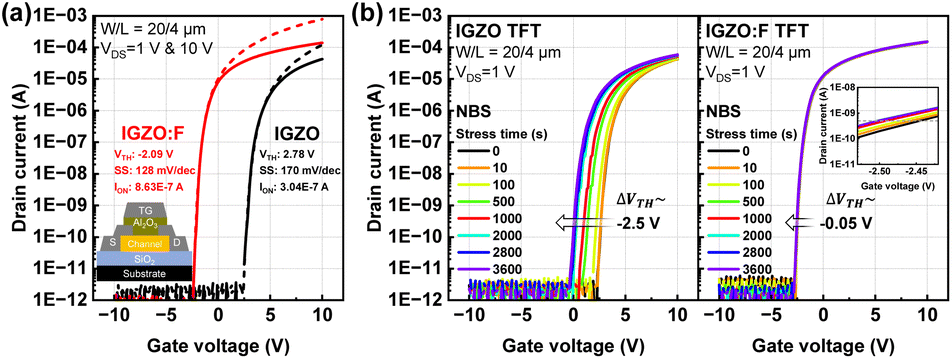 | ||
| Fig. 1 (a) The transfer curves of IGZO and IGZO:F TFTs measured at VDS of 1 V and 10 V. The device structure and electrical parameters are shown in the inset. (b) The NBS results of IGZO TFT (left) and IGZO:F TFT (right) measured at room temperature. The VGS and VDS were −10 V and 0 V, respectively, for stress conditions. The inset in the right panel shows the enlarged transfer curve near the threshold region. | ||
There are two mechanisms if F is introduced into IGZO: oxygen substitution and VO passivation.13,14 The former releases, but the latter consumes electrons, making the resistivity of the thin film lower and higher, respectively. To analyze the energy band structure of the IGZO thin film after F-PDT, UV-vis and UPS characterizations were performed. The optical bandgap was determined from the Tauc plot, and for IGZO and IGZO:F it was 3.52 eV and 3.54 eV, respectively (Fig. 2(a)). Taking the UPS spectra together in Fig. 2(b), the energy band diagrams of the IGZO and IGZO:F thin films are shown in Fig. 2(c). The difference between the conduction band minimum (CBM) and the Fermi level was smaller in the IGZO:F thin film. This implies preferential oxygen substitution over VO passivation in our study, supporting the negative shift of VTH in Fig. 1(a). Under the NBS conditions, near the interface with the dielectric, the probability of VO generation from O is high,33 and the VOs are more stable in a positively ionized state than a neutral state based on first-principles calculations.33 These positively charged species are then trapped at the interface, giving rise to the negative shift of VTH. Therefore, the improved NBS stability reflects the oxygen substitution and VO passivation by F, followed by more stable M–F bond formation.
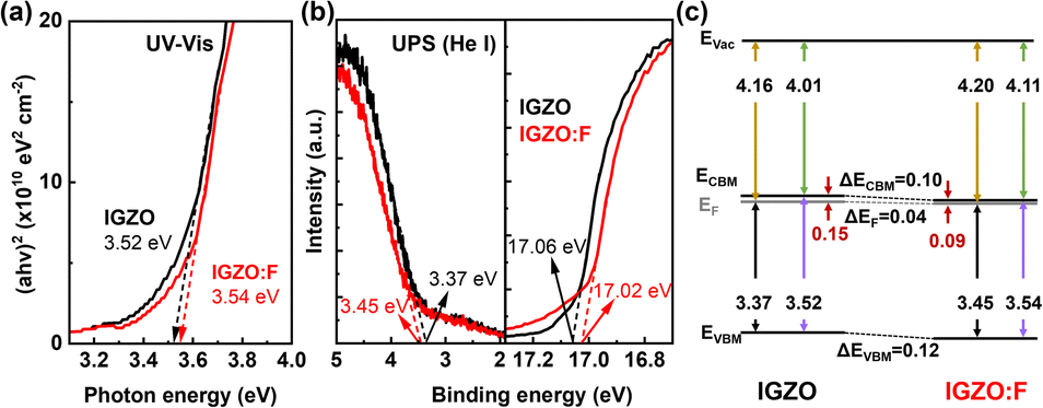 | ||
| Fig. 2 (a) Tauc plots, (b) UPS spectra, and (c) energy band diagrams of IGZO and IGZO:F thin films. | ||
Next, we investigated whether the F can block H diffusion from the Al2O3 into IGZO, because the H plays multiple roles and thereby influences the electrical properties and stability of the TFT. For this purpose, 10 nm-thick Al2O3 was grown by a separate thermal ALD system using ozone (O3) gas, an H-absent oxidant, simply to compare the H concentration. Due to differences in equipment design, the lowest achievable substrate temperature was 180 °C. The TOF–SIMS profiles of as-prepared Al2O3/IGZO stacks indicate that the substrate temperature tuning was more effective in modulating the H-associated concentrations than oxidant modification (Fig. S2(a and b), ESI†). The process at a substrate temperature of 150 °C using H2O oxidant (black), which was our ALD-Al2O3 recipe for TFT fabrication, possessed the highest H-associated concentrations of ALD-Al2O3, followed by significant diffusion into the IGZO. However, given the negligible difference in H-associated concentrations, the F could not function as a barrier against H diffusion (Fig. S2(c and d), ESI†).
Fig. 3 shows the depth-resolved XPS core level raw spectra of Al, O, F, In, Ga, and Zn for Al2O3/IGZO (F) stacks near the interface. Since the Ar+ ion sputtering was performed from the Al2O3 surface, the Al 2p and O 1s spectra obtained at the bulk position are displayed in black. The color maps represent the relative depth of the stacks: from Al2O3 near the interface (red) to IGZO at the bottom (blue). For the Al2O3/IGZO stack in Fig. 3(a), upon getting closer to the interface, the Al 2p and O 1s peaks shifted toward higher binding energy (BE), marked with gray arrows, whereas no prominent shift was observed for other metals (In, Ga, and Zn). However, a pronounced shoulder peak at low BE appeared only in the In 3d5/2 spectra as the position approached the interface. The peak shift toward higher BE in the O 1s spectra near the interface with ALD-Al2O3,30,31 the shoulder peak,28,32 and/or the peak shift30–32 in the metal core level spectra of the underlying metal oxides were the key features in the 2DEG phenomenon induced by the TMA. In other words, the peak shifts in Al 2p and O 1s, and the shoulder peak of In 3d5/2 in Fig. 3(a) are attributed to the chemical reaction of the IGZO surface during the ALD-Al2O3 process. In the case of the quaternary oxide IGZO, the chemical reactions between TMA and all the metal (In, Ga, and Zn) oxides were supposed to be spontaneous based on the thermodynamic calculations.20 In the experiments, the IGZO thin film and IGZO stack covered by ALD-Al2O3 using TMA were compared, and the reduction of the In and Ga species was proposed based on the BE shift toward lower oxidation states (0.13 eV and 0.16 eV for In 3d5/2 and Ga 3d5/2, respectively) according to the XPS surface analysis because of extremely thin Al2O3 (∼2 nm).20 If the IGZO was covered by a metallic Al (∼5 nm) film, which was oxidized into Al2O3 after annealing, the reduction of In ions was solely identified through the presence of shoulder peaks in the In 3d doublet spectra.34 The Ga and Zn spectra were not presented in the literature, with the statement that no obvious change was found.34 In our case, we conducted XPS depth profiling of the IGZO stack covered by thick Al2O3 (∼66 nm) and highlight the shoulder peak in In 3d5/2 spectra as further straightforward evidence for the reduction of In ions. For other metals, the Ga 2p3/2 and Zn 2p3/2 core level spectra at the bottom IGZO were defined as standards and compared with those at upper positions because no significant shoulder peaks were observed in Fig. 3(a). Due to the differences in the composition with respect to the sample depth, the Ga 2p3/2 and Zn 2p3/2 spectra were normalized (Fig. S3(a–d), ESI†). The change in the peak BE values for both Ga 2p3/2 and Zn 2p3/2 spectra was hard to perceive. A weak sub-peak of Ga 2p3/2 at low BE was noticed in the top region, but we believe this cannot confirm the chemical reduction because of noise induced by weak raw intensity. In summary, in the standard Al2O3/IGZO stack, the TMA was oxidized (higher oxidation state) by scavenging O bonding with In near the IGZO surface at the initial stage of the ALD process, driving the peak shifts of the Al 2p and O 1s spectra toward higher oxidation states. At the same time, the In ions were chemically reduced (lower oxidation state) by TMA, being the origin of the shoulder peak at low BE in the In 3d5/2 spectra near the interface. Consequently, it is deduced that the standard Al2O3/IGZO stack in the absence of F-PDT involves interfacial defects of VO and interstitial In (Ini).
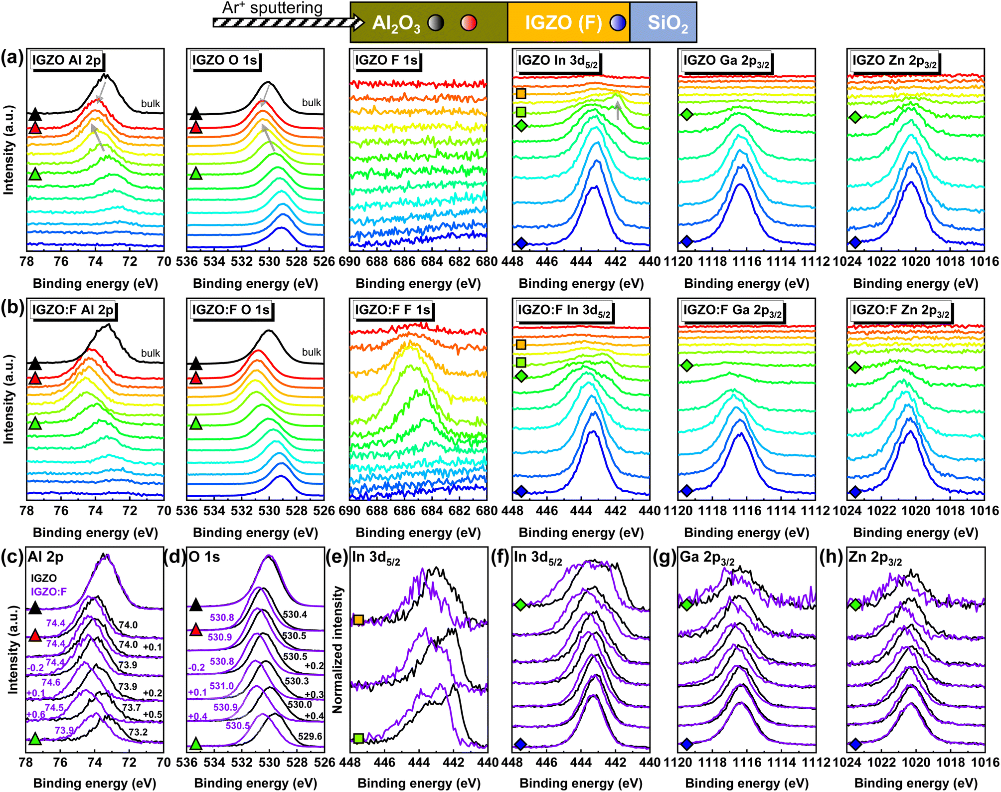 | ||
| Fig. 3 Depth-resolved XPS core level raw spectra of (a) Al2O3/IGZO and (b) Al2O3/IGZO:F stacks after the same Ar+ sputtering time representing Al2O3 at the bulk (black), Al2O3 near the interface (red), and IGZO at the bottom (blue). (c–h) XPS core level raw spectra of elements to compare the impact of F-PDT marked with colored symbols that are the same as in (a and b). (c) Al 2p and (d) O 1s spectra at bulk Al2O3 and near the interface. (e) In 3d5/2 spectra near the interface. (f) In 3d5/2, (g) Ga 2p3/2, and (h) Zn 2p3/2 spectra from the interface to the bottom IGZO. The depth-resolved XPS spectra in (c–h) represent the relative depth of each Al2O3/IGZO (black) and Al2O3/IGZO:F (purple) stack, rather than an exact one-to-one depth comparison between the samples. | ||
Fig. 3(b) shows the depth-resolved XPS core level raw spectra of the Al2O3/IGZO:F stack. The F 1s peak exhibited a higher intensity when approaching the interface. Considering that our full-width half-maximum (FWHM) of the normalized F 1s core level spectra having the high peak intensity was estimated to be ∼3.1 eV (Fig. S3(e and f), ESI†), it is challenging to speculate on the chemical states (see peak BE and FWHM values for In–F, Zn–F, Ga–F, and Al–F bonds in ref. 35). Instead, spectra analysis of the other elements is more beneficial. Fig. 3(c) and (d) compare the Al 2p and O 1s core level spectra with the BE values at the peak positions to emphasize the impact of F-PDT. At the bulk Al2O3, both the Al 2p and O 1s spectra were nearly the same, meaning that the difference in the chemical states for Al and O are almost indistinguishable regardless of the F-PDT. On the other hand, when approaching the interface, the Al 2p and O 1s peaks shifted toward higher oxidation states than those in the Al2O3/IGZO stack. This is not because of an accelerated redox reaction between the IGZO surface and TMA, but due to the chemical shift by F, which has the highest electronegativity and strong oxidizing nature, consistent with the F introduced into Al2O3.36 In other words, the F forms bonds with O and Al. Besides, the native defects of Al2O3 in the proximity of the interface can be occupied by F. In the detailed analysis of Fig. 3(c) and (d), at a depth away from the interface, the peak positions continuously shifted toward higher BE and then were saturated or decreased. For the standard Al2O3/IGZO stack, the maximum BE shifts were 0.8 eV and 0.9 eV for Al 2p and O 1s, respectively. On the other hand, for the Al2O3/IGZO:F stack, the peak position rapidly shifted toward higher BE because of F and then decreased faster, giving rise to the maximum BE shifts of 0.7 eV and 0.5 eV for Al 2p and O 1s, respectively. This indicates that F-PDT interrupts the reducing behavior of TMA, which scavenges oxygen from the IGZO surface. This is also supported by the normalized In 3d5/2 core level spectra near the interface as shown in Fig. 3(e). The shoulder peak observed in the standard Al2O3/IGZO stack was still present despite the F-PDT; however, the lower contribution of low oxidation states was obvious. Therefore, it is inferred that the oxidizing agent F, supplied after IGZO deposition, participates in a chemical reaction with the reducing agent TMA during ALD, alleviating the reduction of In ions and decreasing the number of interfacial defects (VO and Ini). This supports the decrease of the SS and improved stability achieved by IGZO:F TFT in Fig. 1.
Given the above results, the simplest way to counteract the oxygen-scavenging behavior of TMA is to provide supplementary oxygen on the IGZO surface right after its deposition (e.g., post-deposition annealing in air). Another promising approach is to use nitrous oxide (N2O) plasma treatment that has been conducted for mass production.37 Note that N2O exhibits a lower bond order than the diatomic O2 molecule, having a bond order of 2.38 Indeed, the chemical reduction reactions of the underlying IGZO were alleviated as a result of N2O plasma treatment before the ALD-Al2O3 process.20
As mentioned earlier, the VO passivation mechanism has previously been suggested in IGZO with the introduction of F. In particular, it has been confirmed theoretically by first-principles calculations based on density functional theory.39 In experimental work, it is typical to compare by deconvoluting the XPS O 1s core level spectra into three chemical states at a given BE with little tolerance: metal–oxygen (M–O), oxygen-deficient (VO), and hydroxyl group (–OH).15,16,40 However, the O 1s spectra were not deconvoluted in this study, considering several issues in the XPS: secondary chemical shift,41 poor reliability of charge referencing by adventitious carbon (AdC),41,42 and uncertainty of the BE value assignment for the VO chemical state in the metal oxides.43
Besides the interface with the dielectric, C-related impurities in oxide semiconductors can have a detrimental effect on the stability.44 In our samples, no distinct C 1s peak was observed in the IGZO or near the interface, even after the F-PDT using CF4 gas on the IGZO (Fig. S4, ESI†). Regarding the other components of the IGZO upon F-PDT, the normalized core level spectra of all metals (In, Ga, and Zn) are presented in Fig. 3(f–h). The peak BE values near the interface were higher than those in the case of a standard Al2O3/IGZO stack, and then converged to the same values as those closer to bottom IGZO. In other words, the F atoms are likely to be concentrated at the interface with a Gaussian-like distribution, extending to the bottom IGZO, which has a thickness of ∼10 nm. All metals (In, Ga, and Zn) primarily establish bonds with O at the bottom IGZO and partially with F at the top IGZO. Consequently, the high stability of IGZO:F TFT in Fig. 1(b) was also realized by the stable M–F bond formation at the front channel.
Fig. 4(a and b) show enlarged XPS depth profiles near the Al2O3/IGZO (F) interfaces. The F atoms were highly concentrated at the interface, giving rise to the maximum atomic composition of 8.2 at%. It is worth noting that the composition of the interface was In-rich but Ga- and Zn-poor, independent of the F-PDT. This can be attributed to the highest reactivity of TMA with In species, inducing out-diffusion of In toward the interface. From our In 3d5/2 core level spectra showing the shoulder peak even in the case of the Al2O3/IGZO:F stack, the out-diffusion of In could still happen. In addition, the IGZO (F) layers exhibited considerable Al concentration. Nevertheless, further characterization is required to validate these speculations if considering the thickness of the IGZO (F) thin films (∼10 nm) and the principles behind the XPS depth profiling. Taking our case for example, after sputtering the sample in the vertical direction using an Ar+ ion gun (2 keV), X-ray photons emitted by an Al Kα (1486.6 eV) source penetrate into the sample, and the kinetic energies of photoexcited electrons that leave the elements of interest are detected. These sequential procedures are performed repeatedly, collecting narrow-scan spectra of elements as a function of Ar+ sputtering time. One should take into account the (1) atomic mixing during the Ar+ ion sputtering and (2) photoionization cross section and probing depth (typically shorter than 10 nm) of the elements during the XPS analysis.41 The ion bombardment can make surface atoms stick into the film, so atoms at shallow and deep positions are intermixed. In addition, the kinetic energies of photoelectrons from the elements at both shallow and deep positions can be detected simultaneously due to the probing depth. Accordingly, depth-resolved elemental profiles at the interface derived from XPS data may not reflect the precise distributions. To make sure our data were reliable, we conducted (scanning) TEM analysis and EDS line scanning along the interface, to obtain elemental information on the vertically stacked sample in the lateral direction.
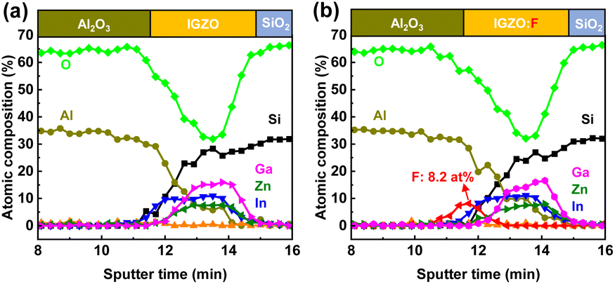 | ||
| Fig. 4 Enlarged XPS depth profiles of (a) Al2O3/IGZO and (b) Al2O3/IGZO:F stacks near the interface. | ||
Cross-sectional TEM bright-field (BF) images in Fig. 5(a and b) show the rough Al2O3/IGZO interface in contrast with the sharp Al2O3/IGZO:F interface. This fully agrees with the depth-resolved XPS analysis that the defect (VO and Ini)-rich Al2O3/IGZO interface was improved as a result of F-PDT because the reduction of In ions vulnerable to the reducing agent TMA was hindered by the oxidizing agent F. Moreover, the EDS line scan profiles in Fig. 5(c) present coherent information that we have inferred from Fig. 4: (i) F atoms concentrated at the Al2O3/IGZO:F interface with Gaussian-like distributions, (ii) In–rich interface, and (iii) Al diffusion into IGZO.
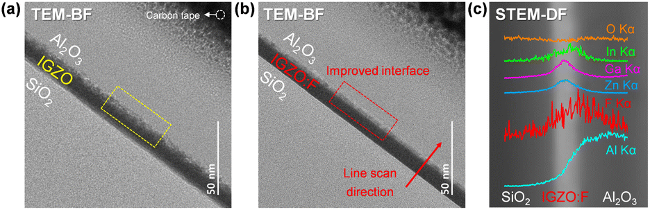 | ||
| Fig. 5 Cross-sectional TEM bright-field (BF) images of (a) Al2O3/IGZO and (b) Al2O3/IGZO:F stacks. (c) Scanning TEM (STEM) dark-field (DF) image of the Al2O3/IGZO:F stack with raw EDS line scan data. | ||
Conclusions
Fig. 6 shows a schematic of the result of F-PDT on IGZO and its relationship with the subsequent ALD-Al2O3 process. At the initial stage of the ALD process, a strong reducing agent, TMA itself, was oxidized by scavenging O, particularly bonding with In at the IGZO surface. This resulted in a rough and defect-rich (VO and Ini) interface between the Al2O3 and IGZO, examined by TEM and depth-resolved XPS, respectively. We employed F, known as a stability enhancer, by substituting O and passivating VO. Given the chemical shifts in the depth-resolved XPS results, stable M–F bond formation was observed for all metals (In, Ga, and Zn), whereas F could not function as a barrier against H diffusion during low-temperature ALD-Al2O3. Nevertheless, F with strong oxidizing character alleviated the chemical reduction reaction of the IGZO surface, establishing a sharp and defect-passivated interface. In summary, a high interface quality was obtained as a result of oxidizing agent supply before the ALD-Al2O3 process. Consequently, improved electrical properties and stability were realized by the top gate TFT configuration. We highlight that, to secure excellent interface quality, the post-deposition oxidation of the IGZO surface should be performed before ALD-Al2O3 process using TMA as a metal precursor.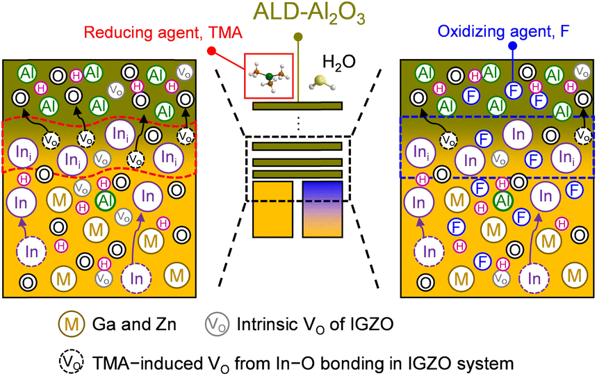 | ||
| Fig. 6 Schematic of F-PDT on the ALD-Al2O3/IGZO stack. | ||
Experimental
TFT fabrication
A thermally grown SiO2/Si substrate was cleaned by acetone, IPA and DI water for 15 min each. After RF sputtering of IGZO (∼10 nm) using a 4-inch ceramic target (In:Ga:Zn = 1:1:1 at%, purity: 4 N) under Ar/O2 (60/1 sccm) plasma, diluted HCl was used for channel patterning. The F-PDT was performed based on CF4/O2 (100/2 sccm) gas for 15 s at a RF bias of 1700 W. The working pressures for IGZO deposition and F-PDT were 5 and 20 mTorr, respectively. E-beam evaporated Ti/Ni stacks were used as S/D electrodes. Next, Al2O3 (∼66 nm) was prepared by a traveling wave type thermal ALD at a growth temperature of 150 °C using TMA and H2O as a metal precursor and oxidant, respectively. After TG (e-beam evaporated Ti/Ni stacks) patterning and subsequent Al2O3 wet etching, the device was annealed by a hot plate at 180 °C for 1 h. All processes were conducted at room temperature except for the ALD and annealing steps. The device structure is shown in the inset of Fig. 1.
Characterization
The electrical properties of the TFTs were measured using a semiconductor parameter analyzer (4200-SCS, Keithley) under ambient conditions and representative parameters were extracted at a VDS of 1 V. Time-of-flight secondary ion mass spectrometry (TOF-SIMS; TOF SIMS 5, ION-TOF) was performed using a primary ion source of Bi+ (30 keV, 1 pA) and a sputtering source of Cs+ (1 keV, 70 nA). The Tauc plots of the thin films were obtained by an ultraviolet-visible (UV-vis; U-2900, Hitachi) spectrophotometer. Ultraviolet photoelectron spectroscopy (UPS; Versaprobe III, PHI) was utilized to quantify the secondary electron cutoff energy and work function using a He I (21.22 eV) source after IGZO surface etching. The atomic compositions and chemical states were analyzed by XPS (Versaprobe III, PHI) using an Al Kα (1486.6 eV) source with Ar+ ion sputtering at an acceleration voltage of 2 keV. Adventitious carbon (AdC) was detected at the sample surface, and the peak BE values for In, Ga, and Zn core level spectra after charge referencing by AdC at 284.8 eV agreed well with the NIST database (Fig. S1, ESI†).45 Nevertheless, in this work, we discuss the BE shifts and features of core level raw spectra with respect to sample depth, rather than focusing on the absolute BE values, because of the uncertainty of charge referencing by AdC.41,42 The chemical shifts are supported by the literature and energy-dispersive spectroscopy (EDS) data, measured by TEM (JEM-2100F, JEOL Ltd) at 200 kV. A focused ion beam (FIB) (Helios 5 UC, FEI) was used for sample preparation.Conflicts of interest
The authors declare no conflict of interest.Acknowledgements
This work was supported by the Samsung Electronics Co., Ltd (IO220817-02058-01) and the Basic Research Laboratory (No. 2021R1A4A3032027) funded by the Korean Government (MSIT).References
- S. Park, S. Seong, G. Jeon, W. Ji, K. Noh, S. Kim and Y. Chung, Adv. Electron. Mater., 2023, 9, 2200554 CrossRef CAS.
- Y. H. Chen, I. T. Wang, Y. M. Zheng and T. H. Hou, presented in part at the 2023 7th IEEE Electron Devices Technology & Manufacturing Conference (EDTM), March, 2023 Search PubMed.
- M. R. Sk, S. Thunder, D. Lehninger, S. Sanctis, Y. Raffel, M. Lederer, M. P. M. Jank, T. Kämpfe, S. De and B. Chakrabarti, ACS Appl. Electron. Mater., 2023, 5, 812–820 CrossRef CAS PubMed.
- A. Belmonte, H. Oh, S. Subhechha, N. Rassoul, H. Hody, H. Dekkers, R. Delhougne, L. Ricotti, K. Banerjee, A. Chasin, M. J. v. Setten, H. Puliyalil, M. Pak, L. Teugels, D. Tsvetanova, K. Vandersmissen, S. Kundu, J. Heijlen, D. Batuk, J. Geypen, L. Goux and G. S. Kar, presented in part at the 2021 IEEE International Electron Devices Meeting (IEDM), Dec, 2021 Search PubMed.
- Y. Zhang, J. Li, J. Li, T. Huang, Y. Guan, Y. Zhang, H. Yang, M. Chan, X. Wang, L. Lu and S. Zhang, Adv. Electron. Mater., 2023, 9, 2300150 CrossRef CAS.
- A. Belmonte, H. Oh, N. Rassoul, G. L. Donadio, J. Mitard, H. Dekkers, R. Delhougne, S. Subhechha, A. Chasin, M. J. v. Setten, L. Kljucar, M. Mao, H. Puliyalil, M. Pak, L. Teugels, D. Tsvetanova, K. Banerjee, L. Souriau, Z. Tokei, L. Goux and G. S. Kar, presented in part at the 2020 IEEE International Electron Devices Meeting (IEDM), Dec, 2020 Search PubMed.
- C. Chen, X. Duan, G. Yang, C. Lu, D. Geng, L. Li and M. Liu, presented in part at the 2022 IEEE International Electron Devices Meeting (IEDM), Dec, 2022 Search PubMed.
- K. Huang, X. Duan, J. Feng, Y. Sun, C. Lu, C. Chen, G. Jiao, X. Lin, J. Shao, S. Yin, J. Sheng, Z. Wang, W. Zhang, X. Chuai, J. Niu, W. Wang, Y. Wu, W. Jing, Z. Wang, J. Xu, G. Yang, D. Geng, L. Li and M. Liu, presented in part at the 2022 IEEE Symposium on VLSI Technology and Circuits (VLSI Technology and Circuits), June, 2022 Search PubMed.
- M. S. Kim, H. T. Kim, H. Yoo, D. H. Choi, J. W. Park, T. S. Kim, J. H. Lim and H. J. Kim, ACS Appl. Mater. Interfaces, 2021, 13, 31816–31824 CrossRef CAS PubMed.
- Y. Jang and S.-Y. Lee, ACS Appl. Electron. Mater., 2023, 5, 509–519 CrossRef CAS.
- J. W. Choi, J. Kim, S. R. Pae, J. Kim, C. G. Kim, H. Lee, S. Ji, S.-W. Nam, Y. K. Lee and B. Shin, Chem. Mater., 2022, 34, 6802–6808 CrossRef CAS.
- A. Zakutayev, J. Mater. Chem. A, 2016, 4, 6742–6754 RSC.
- S. Lee, J. Shin and J. Jang, Adv. Funct. Mater., 2017, 27, 1604921 CrossRef.
- J. Jiang, T. Toda, M. P. Hung, D. Wang and M. Furuta, Appl. Phys. Express, 2014, 7, 114103 CrossRef.
- L. Lu, Z. Xia, J. Li, Z. Feng, S. Wang, H. S. Kwok and M. Wong, IEEE Electron Device Lett., 2018, 39, 196–199 CAS.
- M. Miyakawa, M. Nakata, H. Tsuji, H. Iino and Y. Fujisaki, AIP Adv., 2020, 10, 065004 CrossRef CAS.
- K.-M. Jung, J. Oh, H. E. Kim, A. Schuck, K. Kim, K. Park, J.-H. Jeon, S.-Y. Lee and Y.-S. Kim, J. Phys. D: Appl. Phys., 2020, 53, 355107 CrossRef CAS.
- S. Wang, J. Li, R. Shi, Z. Xia, L. Lu, H. S. Kwok and M. Wong, J. Soc. Inf. Disp., 2020, 28, 520–527 CrossRef CAS.
- W. Pan, Y. Wang, Y. Wang, Z. Xia, F. S. Y. Yeung, M. Wong, H. S. Kwok, X. Wang, S. Zhang and L. Lu, J. Alloys Compd., 2023, 947, 169509 CrossRef CAS.
- J. Li, Y. Zhang, J. Wang, H. Yang, X. Zhou, M. Chan, X. Wang, L. Lu and S. Zhang, ACS Appl. Mater. Interfaces, 2023, 15, 8666–8675 CrossRef CAS PubMed.
- D.-G. Kim, W.-B. Lee, S. Lee, J. Koh, B. Kuh and J.-S. Park, ACS Appl. Mater. Interfaces, 2023, 15, 36550–36563 CrossRef CAS PubMed.
- J. K. Lee, S. An and S. Y. Lee, IEEE Electron Device Lett., 2023, 44, 1845–1848 Search PubMed.
- J. Yang, H. Park, B. Kim, Y.-H. Cho and S.-H. K. Park, J. Mater. Chem. C, 2022, 10, 9699–9706 RSC.
- J. Park, Y. Jang, J. Lee, S. An, J. Mok and S.-Y. Lee, Adv. Electron. Mater., 2023, 9, 2201306 CrossRef CAS.
- J. Kim, T. H. Kim, S. Oh, J. H. Nam, H. Y. Jang, Y. Kim, N. Yamada, H. Kobayashi, S.-Y. Kim, B. H. Lee, H. Habazaki, W. Park and B. Cho, ACS Appl. Electron. Mater., 2020, 2, 1478–1483 CrossRef CAS.
- C. Guerra-Nuñez, M. Döbeli, J. Michler and I. Utke, Chem. Mater., 2017, 29, 8690–8703 CrossRef.
- H. J. Lee, T. Moon, S. D. Hyun, S. Kang and C. S. Hwang, Adv. Electron. Mater., 2021, 7, 2000876 CrossRef CAS.
- T. J. Seok, Y. Liu, J. H. Choi, H. J. Kim, D. H. Kim, S. M. Kim, J. H. Jang, D.-Y. Cho, S. W. Lee and T. J. Park, Chem. Mater., 2020, 32, 7662–7669 CrossRef CAS.
- T. J. Seok, Y. Liu, H. J. Jung, S. B. Kim, D. H. Kim, S. M. Kim, J. H. Jang, D.-Y. Cho, S. W. Lee and T. J. Park, ACS Nano, 2018, 12, 10403–10409 CrossRef CAS PubMed.
- X. Zhu, T. Zhang, Y. He, Y. Liu and H. Zhu, Nanoscale, 2023, 15, 12071–12077 RSC.
- Z. Zhu, T. Yasui, X. Zhao, Q. Liu, S. Morita, Y. Li, A. Yonezu, K. Nagashima, T. Takahashi, M. Osada, R. Matsuda, T. Yanagida and Y. Baba, ACS Appl. Mater. Interfaces, 2023, 15, 36866–36876 CrossRef CAS PubMed.
- S. Y. Lee, J. Kim, A. Park, J. Park and H. Seo, ACS Nano, 2017, 11, 6040–6047 CrossRef CAS PubMed.
- A. de Jamblinne de Meux, A. Bhoolokam, G. Pourtois, J. Genoe and P. Heremans, Phys. Status Solidi A, 2017, 214, 1600889 CrossRef.
- H. Yang, X. Zhou, H. Fu, B. Chang, Y. Min, H. Peng, L. Lu and S. Zhang, ACS Appl. Mater. Interfaces, 2021, 13, 11442–11448 CrossRef CAS PubMed.
- Y. Kawamoto, K. Ogura, M. Shojiya, M. Takahashi and K. Kadono, J. Fluorine Chem., 1999, 96, 135–139 CrossRef CAS.
- S. Lee, D. I. Kim, M. Kim, M. Son, W. Song, S. Myung, H.-K. Jung, S. S. Lee, D. H. Yoon, S. Yim and K.-S. An, Appl. Surf. Sci., 2023, 630, 157464 CrossRef CAS.
- H. Kim, C. Han, D. Kim and B. Choi, IEEE Trans. Electron Devices, 2023, 70, 3611–3616 CAS.
- R. D. Harcourt and A. Schulz, J. Phys. Chem. A, 2000, 104, 6510–6516 CrossRef CAS.
- H. Kawai, H. Fujiwara, J. Kataoka, N. Saito, T. Ueda, T. Enda, T. Ishihara and K. Ikeda, presented in part at the 2020 IEEE International Electron Devices Meeting (IEDM), Dec, 2020 Search PubMed.
- J. G. Um and J. Jang, Appl. Phys. Lett., 2018, 112, 162104 CrossRef.
- G. Greczynski and L. Hultman, J. Appl. Phys., 2022, 132, 011101 CrossRef CAS.
- G. Greczynski and L. Hultman, Prog. Mater. Sci., 2020, 107, 100591 CrossRef CAS.
- T. J. Frankcombe and Y. Liu, Chem. Mater., 2023, 35, 5468–5474 CrossRef CAS.
- Y.-S. Shiah, K. Sim, Y. Shi, K. Abe, S. Ueda, M. Sasase, J. Kim and H. Hosono, Nat. Electron., 2021, 4, 800–807 CrossRef CAS.
- NIST X-ray Photoelectron Spectroscopy Database, NIST Standard Reference Database Number 20, DOI:10.18434/T4T88K, https://srdata.nist.gov/xps/.
Footnote |
| † Electronic supplementary information (ESI) available. See DOI: https://doi.org/10.1039/d3ra06768h |
| This journal is © The Royal Society of Chemistry 2023 |