
 Open Access Article
 This Open Access Article is licensed under a Creative Commons Attribution-Non Commercial 3.0 Unported Licence
Ab initio study of the electronic states of V3Si in momentum space
Saloni Sharma,
Nikhil Joshi,
Vijay Maurya and
K. B. Joshi *
*
Department of Physics, M L Sukhadia University, Udaipur-313001, India. E-mail: cmsmlsu@gmail.com
First published on 30th August 2023
Abstract
The electronic properties of V3Si are reported using the full-potential linearized augmented plane wave method. The electronic properties in the momentum space such as one and two dimensional electron momentum densities and the Fermi surface are presented. The momentum densities are compared with available experimental data. The one-dimensional electron momentum density i.e. the Compton profile is found to be in excellent agreement with the experiment. Anisotropy in the directional Compton profile corroborates the crystalline effects. The dimensions of the Fermi-surfaces are well captured by the 2D electron momentum density. The chemical bonding in this metallic compound is studied by means of the electron localization function and reciprocal form factor which suggest dominance of metallic bonding.
1. Introduction
The A15 compound V3Si is found to be a type-II superconductor with TC = 17.1 K.1 This occurs in cubic structure and acquires a tetragonal structure at temperatures higher than the TC.2 The compound shows multi-band superconductivity. It is a two-band superconductor, discovered well before MgB2.3,4 It is widely used as a stable and durable superconductor. The superconducting wires of this material are used in electric transmission lines, lossless coils, and radio frequency applications because of their operating and capital cost savings, high gradient, and reduced impedance.5Eventually, V3Si has attracted many theoretical and experimental studies.6–18 These include the investigations of the electrical, structural, thermodynamical, and electron–phonon interactions. Since the discovery of this compound, practically major share of the research is devoted to investigate superconductivity because A15 compounds were at the forefront of this fascinating and difficult subject. In essence, there aren't many publications on V3Si other than those pertaining to its superconducting properties that evaluate its ground state properties in momentum space, such as Fermi surface (FS) and chemical bonding, as well as 1D and 2D electron momentum densities (EMD). Although experimental studies of Compton profiles (CP) i.e., the 1D-EMD is reported but no theoretical CP is available for this compound. Therefore, in this endeavour, we attempt ab initio calculations of 1D and 2D-EMD of V3Si which probe electronic states in momentum space. The FS, which is an occupation function in momentum space, is also extensively discussed. The electron localization function (ELF) is a novel approach to explore the nature of chemical bonding in compounds. It is especially suited to study bonding between metallic constituents in a compound. We perform the study of chemical bonding using ELF and discuss it in conjunction with the charge transfer reported by the number of workers6,19–23 and the reciprocal form factor. The latter is a transformation of Compton profile in real space. In the highly pure A15 crystals of the A3B type, interestingly, the movement of B atoms is restricted. On the other hand, A atoms can move on its sub-lattice by exchanging positions with the vacancies present on the same sub-lattice. The diffusion of B is only possible depending on the presence of B antisite defects and vacancies on the lattice. Therefore, the diffusion in these structures is quite important. In fact, interchangeability of atoms at the A and B sites is the reason why diffusion is very critical in A15 compounds. This aspect of the A15 compounds has not been touched upon. In this endeavour, we push the boundary of our current understanding of diffusion and related properties further by evaluating the vacancy migration enthalpy.
Both 1D and 2D-EMD are unique observables. These can be calculated as well as measured. These two unravel the momentum space behaviour of the ground state of a material. The CP is directly related to the momentum density distribution of the system. As CP is sensitive to the behaviour of valence electrons, many characteristics of solids owing to valence electrons can be probed. The results of CP give the valuable information about the Fermi surface and its dimensions, correlation effects in transition metal compounds, and the nature of chemical bonding.24–27
In the independent particle model (IPM), the wave function of band electrons in momentum space ψkn(p) can be obtained as:
 | (1) |
 | (2) |
 | (3) |
 | (4) |
The anisotropy can be extracted by taking differences in the DCPs determined along [hkl] and [h′k′l′] directions. Thus anisotropy is:
| ΔJAni.(pz) = Jhkl(pz) − Jh′k′l′(pz). | (5) |
The anisotropies deliver information about the occupied bands via fkn, and Fermi surface in metals and related systems.28
The Compton profile J(pz), signifies the probability that the scattering electron has a component of momentum (pz). Moreover, this is a projection of the EMD ρ(p) along the scattering vector (z-axis). From the measurement point of view, within the validity of impulse approximation, the Compton profile is related to scattering cross section as follows:29
 | (6) |
 where N is the number of electrons participating in the Compton scattering in a given geometry.
Pattison and Williams31 have proposed an alternative approach to interpret the CP data. The Fourier transform of the Compton profile contains information related to Fermi surfaces and bonding. The Fourier transform of the CP is defined as:
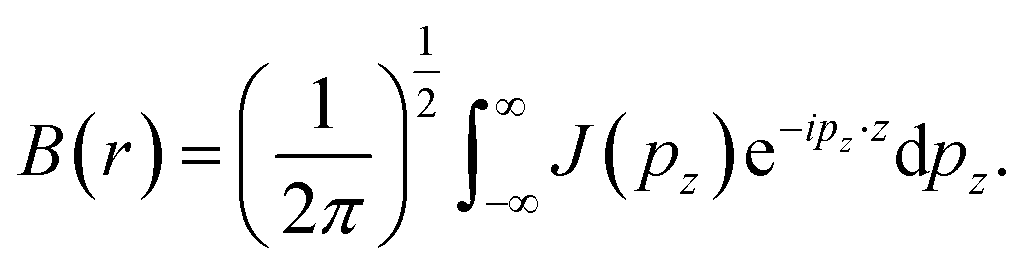 | (7) |
For free electron gas, the B(r) function is given by:
 | (8) |
The B(r) is known as the auto-correlation function or the reciprocal form factor. It carries information regarding Fermi surfaces and bonding. In the case of metals, the free electron behaviour leads to the parabolic shape of the CP. This feature manifests as a zero value of B(r) wherever pfr = 4.493, 7.725, 10.904, 14.066 etc.31,32 In compounds with completely filled shells the B(Rj) = 0 at lattice translation vectors.33–37 The minimum in the B(r) function signifies the bond length.38
The 2D-EMD is another interesting property that can be determined both experimentally as well as theoretically. This can be probed via the two-dimensional angular correlation of annihilation radiation (2D-ACAR) technique, which is also very sensitive to the valence electrons. It is evaluated by the integral of EMD ρ(p) or the two-photon momentum density (TPMD), denoted by ρ2γ(p) along a single direction. However, it is affected by the influence of the positron. In crystalline solids, the annihilation of Bloch-state positrons with electrons leads predominately to the emission of two photons.39 In 2D-ACAR measurements, one measures the 2D-projection of the TPMD. Observing the annihilation radiation provides information about the electronic structure in the momentum space.29,39,40 This can be calculated from the squared absolute value of the Fourier transform of the wave function of electrons ψkn(r) and positrons function ψp(r) denoted here as ρ2γ(p). In the independent particle approximation:
 | (9) |
 | (10) |
To understand the nature of bonding from the perspective of Lewis theory, the unique contemporary theoretical tool ELF is introduced. It enables to unfold of the physics of inter-phase and intraphase phenomena.41,42 It pinpoints the areas in atomic, molecular, and crystalline systems where electrons are localised. Mulliken43 first envisioned the division of space into non-overlapping regions based on ELF theory, which Bader, Luken, and Culberson later refined.44,45 ELF is viewed as the inverse probability of finding two same spin electrons at a given point in space. The spin-paired states i.e., the low probability regions are well localized and show a larger ELF, while the unpaired states i.e., the regions of high pair probability or the regions of like spin electrons, are poorly localized and show a lower ELF.46 In the formulation, the ELF is defined as a ratio between the excess of kinetic energy density resulting from the Pauli exclusion principle D(r), and the kinetic energy density of homogeneous electron gas D0(r) as:41,46,47
 | (11) |
Within the Kohn–Sham scheme, the increase in kinetic energy can be written as:
 | (12) |
 | (13) |
The ELF, normally denoted by η(r), is given by:
| ELF = η(r) = [1 + χ(r)2]−1. | (14) |
The ELF takes values between 0 and 1. Generally, ELF is drawn on a plane, and the value of the function is projected by colour. The lowest permissible value is 0, which highlights delocalized bonding. The maximum possible value of ELF (= 1) corresponds to the highest degree of electron localization i.e., ELF is higher in the region where bonds and lone pairs are formed. For metals, eqn (11) yields χ(r) = 1, suggesting the  which signifies perfect delocalization.41,48–50 Insulators are often considered to be composed of localized bonds and metals of delocalized bonds. Thus, ELF can differentiate among metallic, covalent, and other bonding regions.
In this work, we have studied the 1D and 2D-EMD as well as the Fermi surface of V3Si. The 1D-EMD i.e., Compton profile of polycrystalline V3Si is compared with the available experimental data reported by Sharma et al.22 The anisotropies in the DCPs of V3Si are reported for the first time. The 2D-EMD is compared with the 2D-ACAR measurements reported by Farmer et al.51 The nature of bonding is examined using the reciprocal form factor, charge transfer, and the ELF. The findings of the Fermi surface are compared with available experimental results.52 The article is organised as follows: the basic details of the calculations are given in Sec. 2. The discussions of the results of the Compton profile, 2D-EMD, ELF and Fermi surface are given in Sec. 3. Finally, conclusions are given in Sec. 4. Unless otherwise stated, all quantities are described in atomic units (a.u.), where e = ℏ = m = 1 and c = 137.036, giving unit energy equivalent to 27.212 eV, unit momentum equivalent to 1.9929 × 10⁻²⁴ kg m s−1. The last one is close to the momentum of an electron at the Fermi surface in aluminum, and the unit length is equal to the Bohr radius 0.52917 × 10⁻¹⁰ m.
2. Computational details
The crystal structure of V3Si belongs to the space group Pm![[3 with combining macron]](https://www.rsc.org/images/entities/char_0033_0304.gif) n (#223). There are eight atoms in the unit cell. The V atoms follow the point symmetry
n (#223). There are eight atoms in the unit cell. The V atoms follow the point symmetry ![[4 with combining macron]](https://www.rsc.org/images/entities/char_0034_0304.gif) 2m and occupy 6c Wyckoff positions. The Si atoms follow the point symmetry m3 and occupy 2a Wyckoff positions. We deployed the full potential linearised augmented plane wave (FP-LAPW) method founded on the density functional theory.53 The mathematical framework and overall scheme of the FP-LAPW and allied methods can be found elsewhere.54 For the exchange correlation functional, we have used the Perdew–Burke–Ernzerhof (PBE) ansatz based on generalized gradient approximation (GGA).55 The muffin-tin radii were 2.198 Bohr and 2.200 Bohr for V and Si atoms, respectively. The plane wave cut-off parameter rgkmax was set to 8.5. The charge and energy self-consistent calculations were performed taking the Monkhorst–Pack net of 20 × 20 × 20 size. The LAPW method embodied in the Elk allows us to calculate the 1D-EMD, 2D-EMD and the ELF.53 The EMD calculations are performed with hkmax = 20 a.u. This was found to be sufficient to satisfy the normalisation of the valence Compton profile of V3Si. The calculated ELF is plotted using VESTA,56 and the Fermi surface is plotted using XCrysden.57 For the calculations of DCP, the three principal crystallographic directions [100], [110], and [111] are undertaken.
2m and occupy 6c Wyckoff positions. The Si atoms follow the point symmetry m3 and occupy 2a Wyckoff positions. We deployed the full potential linearised augmented plane wave (FP-LAPW) method founded on the density functional theory.53 The mathematical framework and overall scheme of the FP-LAPW and allied methods can be found elsewhere.54 For the exchange correlation functional, we have used the Perdew–Burke–Ernzerhof (PBE) ansatz based on generalized gradient approximation (GGA).55 The muffin-tin radii were 2.198 Bohr and 2.200 Bohr for V and Si atoms, respectively. The plane wave cut-off parameter rgkmax was set to 8.5. The charge and energy self-consistent calculations were performed taking the Monkhorst–Pack net of 20 × 20 × 20 size. The LAPW method embodied in the Elk allows us to calculate the 1D-EMD, 2D-EMD and the ELF.53 The EMD calculations are performed with hkmax = 20 a.u. This was found to be sufficient to satisfy the normalisation of the valence Compton profile of V3Si. The calculated ELF is plotted using VESTA,56 and the Fermi surface is plotted using XCrysden.57 For the calculations of DCP, the three principal crystallographic directions [100], [110], and [111] are undertaken.
3. Results and discussion
3.1 Structural properties
The calculations are performed at the equilibrium lattice constants, obtained by fitting the Murnaghan equation of state to the computed data set of total energies. We find the lattice constant a = 4.706 Å and bulk modulus B0 = 188.70 GPa. Both are in very good agreement with the available experimental lattice constant a = 4.72 Å and bulk modulus B0 = 196 GPa.58Interestingly, the elastic constants enable us to find the tendency of materials to form vacancies, migrate and undergo diffusion. This is of practical interest in technological applications where annealing and deformation procedures are required in the fabrication processes. The vacancy migration enthalpy HM is defined as:59
| HM = δ2GFa3, | (15) |
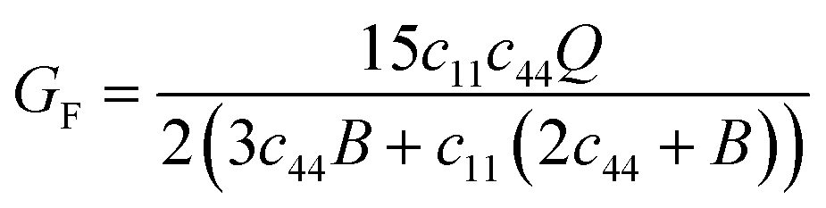 and Q = (c11 − c12). Using the reported values of elastic constants60 and taking the value of δ2 = 0.022 prescribed for cubic crystal structures, one can compute HM. For V3Si, it turns out to be 1.951 eV. Using high throughput calculations, the following relation has been suggested by Angesten and co-workers:61
| HM = 0.016B0a3, | (16) |
3.2 Electronic states
The electronic band structure of V3Si is shown in Fig. 1. The shell wise contributions of V and Si atoms in the formation of bands can be analysed from the partial DOS plotted in Fig. 2(a) and (b). The band structure can be divided into three regions ranging from −5.16 to −2.52 eV, −2.52 eV to Fermi level (EF), and EF to 3.15 eV. In the −5.16 to −2.52 eV region, most of the bands are well dispersed, while a few show less dispersion in Γ–X, X–M, M–Γ and Γ–R lines. Therefore, a peak below −4 eV appears in the DOS. In Fig. 2, we note that the V(d) and Si(p) states contribute to this peak. There is a minor contribution from the V(s) and V(p) states also.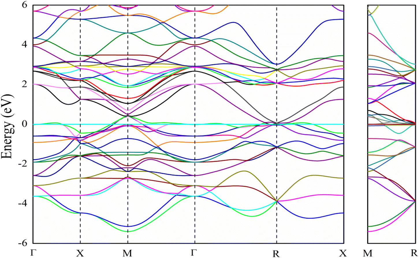 | ||
| Fig. 1 Band structure of V3Si. | ||
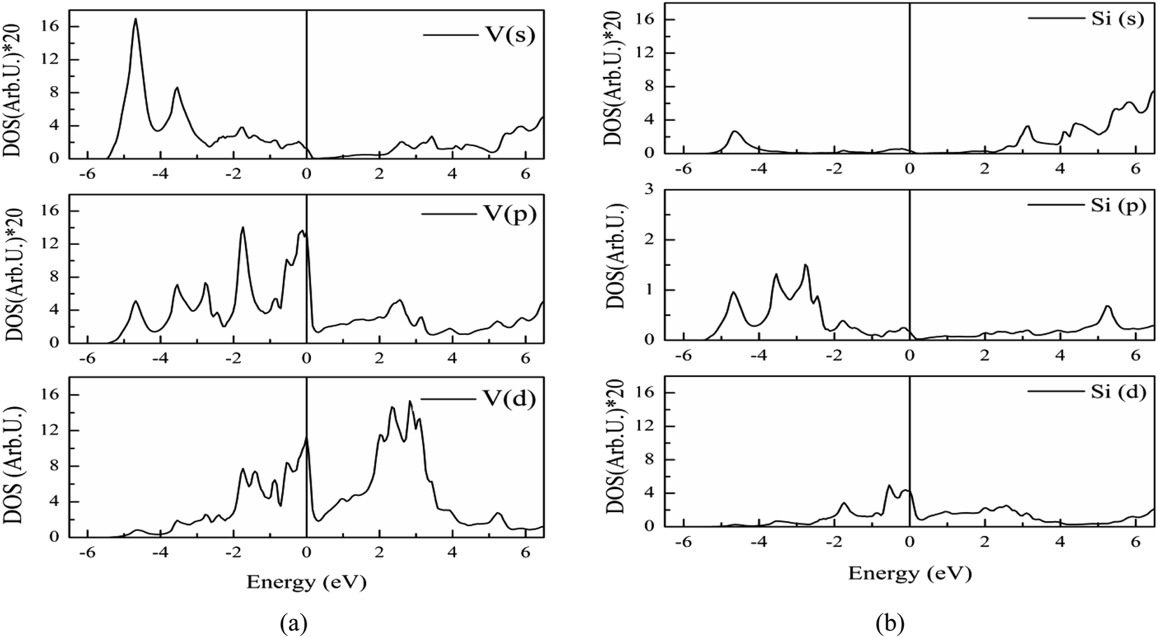 | ||
| Fig. 2 Partial DOS from s, p and d states of (a) vanadium, (b) silicon atoms in V3Si. To improve visibility the scale of DOS in case of V(s), V(p), Si(s) and Si(d) is multiplied by 20. | ||
In the −2.52 to EF region there are some flat bands that cause a rapid fall of the DOS near the EF. These flat bands originate predominantly from the V(d) states and partially from the V(p) states. At Fermi energy, three flat bands extend in the M–Γ–R segment. These contribute to the N(EF) sharpness and also play a significant role in shaping the FS which will be discussed later. This feature is also a signature of the superconducting behaviour of V3Si seen in A15 compounds.3,13,63 Overall, the band diagram suggests V3Si to be a conductor. A high value of N(EF) is reported by a number of workers in V3Si. In current work, the N(EF) is found to be 224.79/(Ry. per unit cell), which is in very good agreement with the earlier result using the FP-LAPW i.e., 222.10/(Ry. per unit cell).64
The region from EF to 3.15 eV shows very large dispersion, resulting in a large bandwidth of the conduction bands, which originates mainly from the V(d) states, followed by some contribution from other valence states of V and Si. In the region 2–4 eV, many bands gather, which are less dispersed, resulting in numerous peaks. These are again dominated by V(d) states. Thus, V(d) states largely affect the overall band structures and hence the electronic states of the V3Si.
3.3 Fermi surface
The four bands contribute to the formation of the FS of V3Si.65 Band-by-band decomposition of the FS is shown in Fig. 3. The irreducible Brillouin zone with the high symmetry k points is drawn in Fig. 3(a). A bird eye view of the region of bands, dispersing in the range of −0.5 to 0.5 eV around EF, contribute to the shapes of Fig. 3(a)–(d), is given in Fig. 4. Both the FS and the contributing band dispersion curves resemble the findings from the VASP by Cho et al.3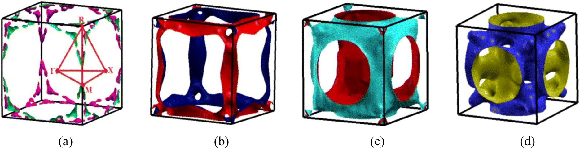 | ||
| Fig. 3 The Fermi surfaces of V3Si from (a) first (b) second (c) third and (d) fourth band. | ||
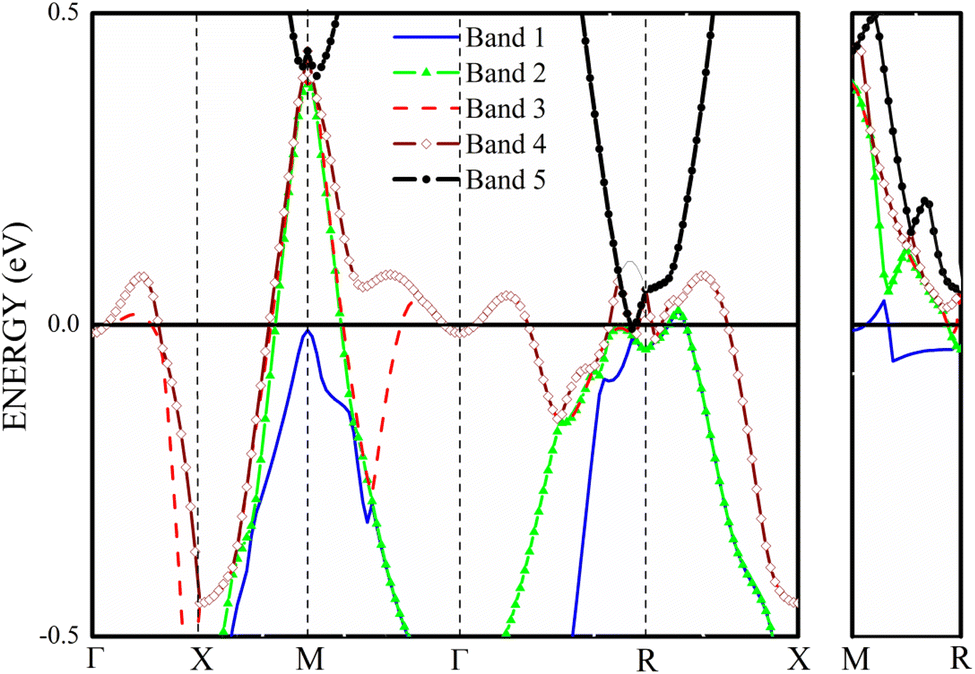 | ||
| Fig. 4 The band structure of V3Si in −0.5 to 0.5 eV range. | ||
The FS due to the first band shown in Fig. 3(a) is hole-like. It has a small hole-like structure extending over a very small region beginning at 0.076 (π/a) in the R → X direction. As Fig. 4 depicts, the first band crossing the Fermi level around the R point gives rise to this shape. The FS due to second band, shown in Fig. 3(b), is also hole-like. Similar to the first band it extends over a small region in the R → X and R → Γ directions. Unlike the first band, however, the FS due to the second band extends in the Γ → M and M → X directions also. The hole like structure begins in the Γ → M direction at 0.39 (π/a) and truncates in the M → X direction at 0.12 (π/a). These features give rise to laminar structure along the M–R edge. The upper two bands cross the Fermi level at several points and hence give rise to the complex shape of the Fermi surfaces drawn in Fig. 3(c) and (d). These arise from the third and fourth bands. These bands have multiple sheets arising from the crossings in the Γ–X, X–M, M–Γ, Γ–R and M–R lines. Both the third and fourth bands form nearly identical sheets, except in the M–Γ–X line. As observed in the earlier studies, the protuberances or bulges are visible towards the R points.65 The third band constitutes a large hole pocket at the Γ point like a deformed sphere. The radius of the deformed circle in the M–R–X plane is 0.24 (π/a) in the X–M direction and 0.36 (π/a) in the X–R direction. Notably, deformed radii of 0.2 (π/a) and 0.4 (π/a) observed by the 2D-ACAR data are close to our results in comparison to earlier first principles studies.51,52 FS due to the fourth band has a hole-like surface around M point with openings towards the Γ point forming a jungle-gym structure.65 The dispersion of the third and fourth bands in the X–M–Γ line marks the difference in the FS drawn in Fig. 3(c) and (d). Note that the third band becomes electron-like at 0.11 (π/a) in the M–Γ direction, turns into hole-like at 0.3 (π/a) and becomes electron-like again at 0.416 (π/a) near the Γ point. On the contrary, the fourth band remains hole like up to 0.416 (π/a) near the Γ point. The third and fourth bands show similar features up to 0.49 (π/a) in the Γ–R direction. These constitute electron lenses of small size up to 0.06 (π/a), followed by hole like sheets up to 0.23 (π/a). Thereafter, the sheets are electron-like up to 0.49 (π/a) in the Γ–R direction. Beyond this, for a very small interval, the surface becomes electron-like, which gives rise to the bulges in the Γ–R direction.
3.4 Electron momentum density
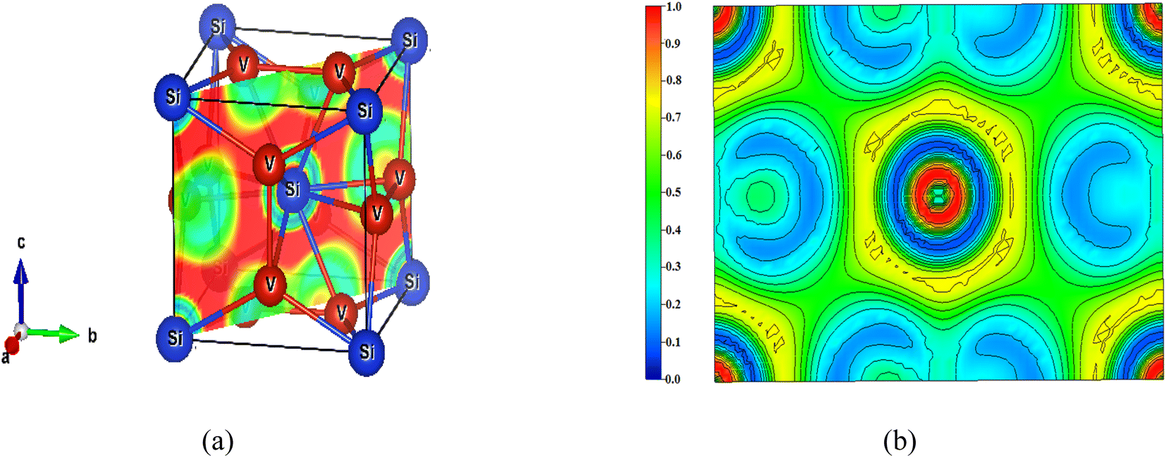
As introduced, the Compton scattering and the 2D-ACAR measurement directly measure the EMD. The Compton scattering delivers the 1D projection of the EMD, whereas the 2D-ACAR measures the integral along a single direction i.e., the 2D projection of the TPMD, which is closely connected to the EMD but includes the influence of the positron. Such studies are quite useful for studying electronic states in bulk.39 Here in follows the comparison between our calculations and the published measurements.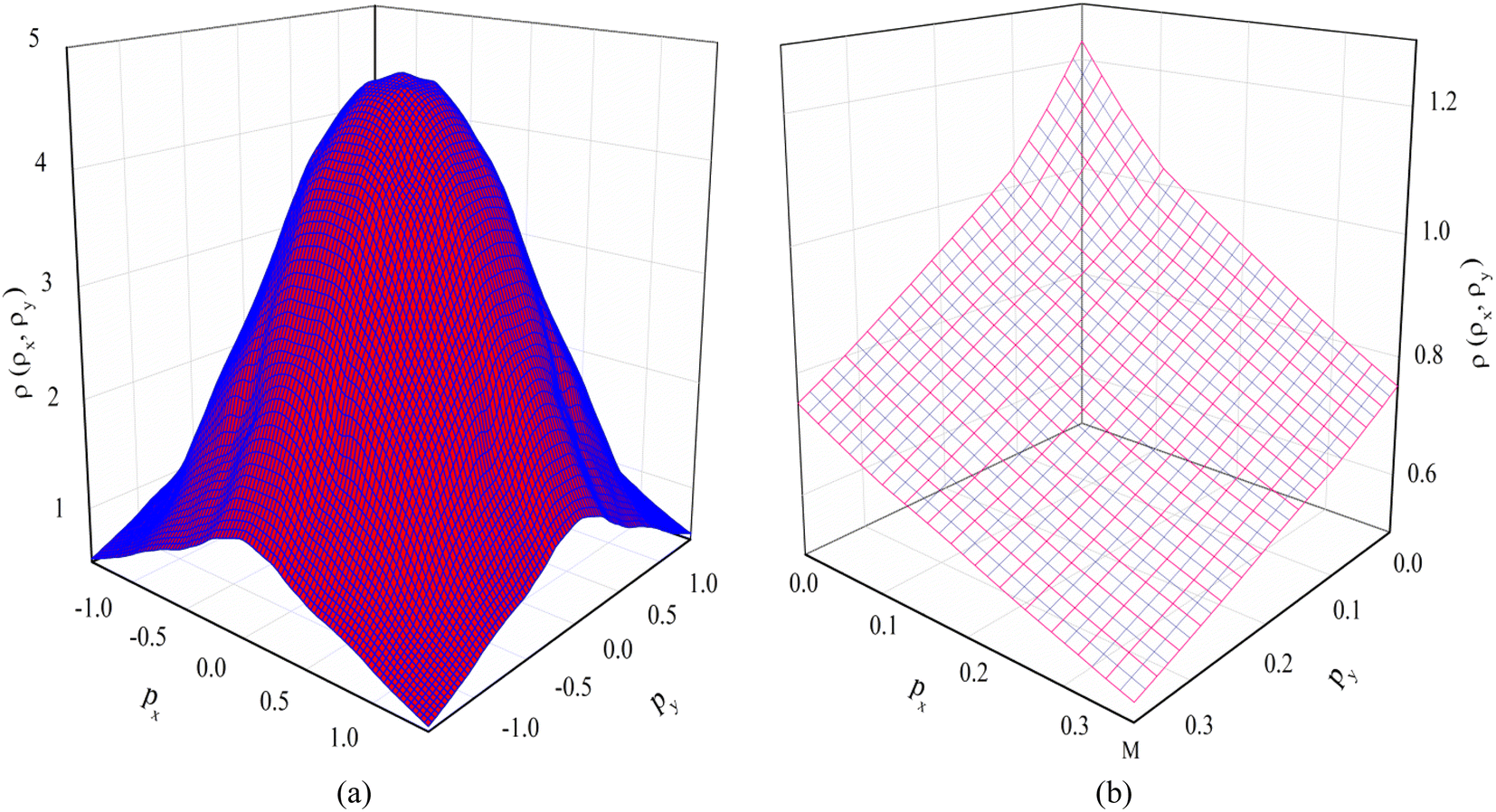 | ||
| Fig. 5 The calculated 2D-EMD of V3Si. (a) The 2D-EMD view and (b) The selective projection on the px − py plane. | ||
Isotropic Compton profiles. Sharma et al.22 have published experimental CP of the polycrystalline V3Si. They have reported total isotropic experimental CP using a 59.54 keV γ-ray Compton spectrometer. Our calculation gives the valence electron CPs. To extract the experimental CP due to valence electrons, the core contribution, taken from the tables of Biggs et al.66 is subtracted. All the valence profiles are then normalised to 21.083 electrons in the 0–7 a.u. range and convoluted with a Gaussian resolution function taking 0.53 a.u. width. The Elk delivers the directional Compton profile. For the polycrystalline material, the spherical average of CP is required to get the isotropic CP. This is deduced by taking the average using the 3D-Sphav formula described in earlier studies.67–69
In Fig. 6, the measured and calculated CPs of valence electrons are plotted. The difference ΔJ(pz) = Jtheory(pz) − Jexperiment(pz) is shown in the lower panel. In the 0 ≤ pz ≤ 0.7 region, the theory underestimates the CP thereafter it overestimates up to 1.5 a.u. The maximum difference visible at 0.3 a.u. is 2.4% of JVal.Expt.(0). Beyond 1.5 a.u., the ΔJ is well within error bars. Beyond 3 a.u., the difference is very close to zero, as this is the region dominated by core electrons, which are absent in the valence CP. The point-by point resemblance of theory and experiment in this region highlights that the current calculations are in very good agreement with the experiment.22
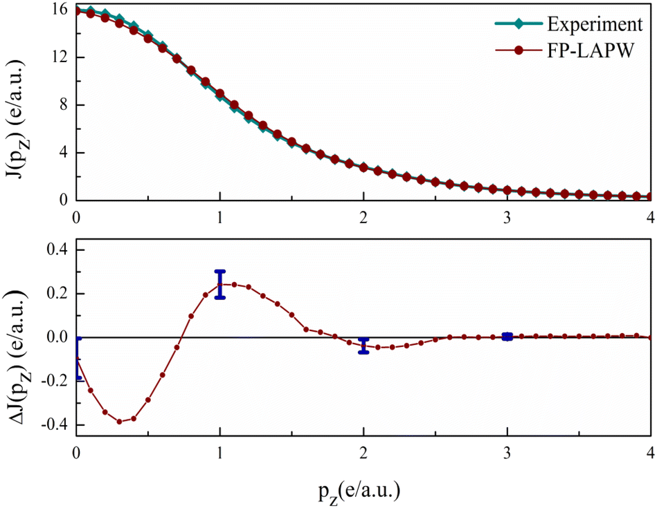 | ||
| Fig. 6 The experimental and theoretical valence Compton profiles of V3Si are shown in the upper panel. The difference curve ΔJ(pz) = Jtheory(pz) − Jexperiment(pz) is shown in the lower panel. Experimental errors are also indicated at some points. | ||
Anisotropies. The DCPs calculated along principal directions [100], [110], and [111] are normalised to 21.083 electrons in the 0–7 a.u. range. To get the anisotropies, the differences in the DCPs are found. The three anisotropies derived from the unconvoluted DCPs are plotted in Fig. 7.
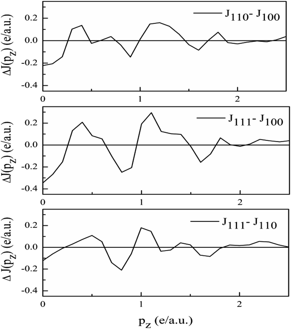 | ||
| Fig. 7 Anisotropies in the unconvoluted directional Compton profiles of V3Si using the GGA. | ||
As the band structure shown in Fig. 4 depicts, the electron and hole-like sheets contribute to the DCPs and hence the anisotropies. The Γ–X line has electron-rich sheets. The Γ–M and Γ–R have both hole- and electron-rich sheets. So the J111 − J100 is maximum at pz = 0. The maximum values of the two anisotropies with respect to [100] are 0.21 and 0.32 e a.u.−1, respectively at pz = 0. These are about 2% of JVal.Expt.(0), which can be well measured at the synchrotron radiation facilities. In terms of occupancy, the occupied states at pz = 0 are more in [100], followed by [110] and [111]. In the anisotropy curves, the positions of the extrema are clearly visible. The maxima in the J111 − J100 and J110 − J100 occur around  and
and  Moreover, the J100 has more contribution at
  So both anisotropies show reduced contributions at this momentum. Beyond 2 a.u., the anisotropies vanish because only the isotropic contribution of electrons prevails, which is cancelled by the differences in the DCPs.
3.5 Electron localization function and bonding
The nature of bonding in V3Si has been studied by a number of workers on the basis of charge density plots, which were devoid of either charge or energy self-consistency due the smaller number of k points used in the computation. The experimental studies are performed using Compton scattering and X-ray diffraction measurements.22,70 As described before, ELF is now a useful technique to study the nature of bonding in compounds. As illustrated earlier, the lowest permissible value of ELF points out delocalized bonding; the maximum value of ELF corresponds to the highest degree of electron localization; and ELF = ½ signifies perfect delocalization.41,48–50In Fig. 8, the crystal structure and the ELF in the (100) plane at x = 0.5 and 1 units are drawn. The enlarged views are shown in Fig. 8(b) and (c). The ELF from the Si atom can be seen at the centre in Fig. 8(b). A very high value of ELF ∼ 1 is visible around this position, which decreases rapidly in all directions. This points out highly localised charges around the Si atom, suggesting the formation of bonds and lone pairs. The two locations on the c-axis and its parallel edge also show localised charges that arise from the vanadium atoms situated just below and above this (100) plane. On either side of the locations in the b-direction where ELF = 0.3, the vanadium atoms are situated. In this entire region, ELF lies in the 0.3 ≤ n(r) ≤ 0.5 range, suggesting dominant metallic bonding. One can see that the upper and lower edges of the hexagon are directed towards the vanadium atoms located in the direction of the b-axis. The ELF = 0.5 points out that the V–Si bond is largely metallic. Notably, more delocalized charges in the vicinity of vanadium than silicon point out Si to V charge transfer. The middle edges of the hexagon are directed towards the middle of the V–V bond on the faces of the cube perpendicular to the (100) plane. Here the ELF = 0.3. Thus, in this plane, the ELF around vanadium atoms is ½ suggesting metallic bonding.
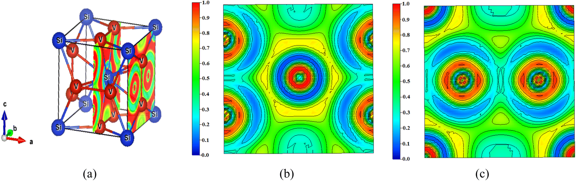 | ||
| Fig. 8 (a) Crystal structure of V3Si showing the (100) planes at x = 0.5 and x = 1 and the ELF. The enlarged views of the ELF in the two planes are shown in (b) and (c). | ||
In the (100) plane at x = 1 the four quartets at the corners of the plane are due to silicon atoms showing highly localised ELF. Around the two vanadium atoms in the plane, the ELF is again in the 0.3 ≤ n(r) ≤ 0.5 range, pointing to delocalization of charges due to the dominating metallic behaviour of the V–V bond. The yellow channels (ELF = 0.75) around the silicon quartets on four corners of the plane constitute the hexagon visible at the centre in Fig. 8(b).
The ELF on the (110) plane and the enlarged view are shown in Fig. 9. The ELF at the centre and the four corners, clearly visible in Fig. 9(b), arise from the silicon atom. ELF signifies highly localised charges around the silicon, which gradually get delocalized in all directions. As the plane passes through the V–V bond, the ELF is within the 0.1 ≤ n(r) ≤ 0.3 range, suggesting charge delocalization. The major part of the (110) plane is green, indicating ELF = ½. This points out that the electron density is more like the homogeneous electron gas, pointing to metallic bonding. The outer part of the ELF around the silicon atom shows ELF in the 0.7 ≤ n(r) ≤ 0.8 range suggesting covalent bonding. Both planes point out prominent metallic behaviour accompanied by some charge transfer from silicon to vanadium.
 | ||
| Fig. 9 (a) The (110) plane of V3Si and (b) the ELF with scale. | ||
Several authors have studied charge transfer using experiments and ab initio methods.6,19–23 These are summarised in Table 1. These point out charge transfer from either V to Si or Si to V. In the crystalline state, the charge within the MT sphere is 21.25 and 12.36 electrons on vanadium and silicon, respectively. The charge in the interstitial region is 13.77. The charges found by earlier calculations on vanadium and silicon within the MT sphere were 21.29 and 12.46 electrons, respectively.20 In contrast, in the interstitial region of the crystal the charge i.e., 13.34 was less. The ELF described above also points out that most of the vanadium electrons show a delocalized nature spread in the interstitial region, forming metallic bonds, which was not considered in earlier studies.
Now we discuss the bonding characteristics of V3Si in terms of the B(r) function. The reciprocal form factor i.e., B(r) is plotted in Fig. 10. The minimum in B(r) corresponds to the bonding length, whereas the zero positions give the Fermi momentum. The calculation gives the minima at 4.46 a.u. while the experiment gives the minima at 4.65 a.u. In both cases, the minimum occurring at about half of the lattice constant shows good agreement.
 | ||
| Fig. 10 The B(r) function of V3Si. | ||
The B(r) from FP-LAPW intersects the r-axis at a number of positions. In metallic systems, the first intersection occurs at pfr = 4.493 and the next at pfr = 7.725. These yield values of pf to be 0.81 a.u. and 0.84 a.u., respectively. These are very close to the calculated value 0.88 a.u. This suggests that the B(r) function also captures the free electron-like or metallic behavior of electrons in V3Si.
In the region beyond 6 a.u., there are some differences in the B(r) function between theory and experiment. To incorporate the effect of the resolution function into theory, the B(r) function has to be multiplied by the damping function. This will attenuate the B(r) function beyond 6 a.u. and may bring the shape of B(r) function closer to the experimental shape.
4. Conclusions
The electronic properties of V3Si in the momentum space are studied using FP-LAPW calculations in this work. The results of band structure and partial DOS point out the dominance of V(3d) states. The flat bands in the −2.52 to EF region originate mainly from the V(3d) and partially from the V(3p) states. The calculated value of N(EF) is found to be in very good agreement with the earlier calculations. The shape and dimensional characteristics of the Fermi surfaces resemble with the available experimental results. The findings of the 2D-EMD are consistent with those of the 2D-ACAR. The calculated directional CP and anisotropies reveal the salient features of the band structure around Fermi energy and the Fermi surface. The maximum anisotropy is 2.4% of JVal.Expt.(0). The isotropic Compton profile is found to be in very good agreement with the experimental profile. The nature of bonding in V3Si is discussed using ELF and B(r) function. In the (100) plane, highly localised charges around the Si atom and delocalized charges in the vicinity of vanadium are found, which suggest charge transfer from Si to V. The ELF in both planes suggests metallic behaviour accompanied by some charge transfer from Si. The B(r) function suggest a strong V–Si bond with a bond length of about half of the lattice constant. The function also captures the dominant metallic behaviour of electrons by projecting the accurate value of pf.Conflicts of interest
There are no conflicts to declare.Acknowledgements
This work is partially supported by RUSA 1.0 program of MHRD New Delhi, India.References
- M. Heilper, J. Ashkenazi and J. Felsteiner, Phys. Rev. B: Condens. Matter Mater. Phys., 1986, 33, 755 CrossRef CAS PubMed.
- S. Tanaka, A. Miyake, B. Salce, D. Braithwaite, T. Kagayama and K. Shimizu, J. Phys.: Conf. Ser., 2010, 200, 012105 CrossRef.
- K. Cho, M. Kończykowski, S. Ghimire, M. A. Tanatar, L. Wang, V. G. Kogan and R. Prozorov, Phys. Rev. B, 2022, 105, 024506 CrossRef CAS.
- A. Perucchi, D. Nicoletti, M. Ortolani, C. Marini, R. Sopracase, S. Lupi and P. Dore, Phys. Rev. B: Condens. Matter Mater. Phys., 2010, 81, 092509 CrossRef.
- S. Deambrosis, G. Keppel, V. Ramazzo, C. Roncolato, R. Sharma and V. Palmieri, Phys. C, 2006, 441, 108 CrossRef CAS.
- G. Arbman and T. Jarlborg, Solid State Commun., 1978, 26, 857 CrossRef CAS.
- G. Bilbro and W. L. McMillan, Phys. Rev. B: Solid State, 1976, 14, 1887 CrossRef CAS.
- W. E. Blumberg, J. Eisinger, V. Jaccarino and B. T. Matthias, Phys. Rev. Lett., 1960, 5, 149 CrossRef CAS.
- T. Chihi, M. Fatmi and M. Ghebouli, Phys. B, 2012, 407, 3591 CrossRef CAS.
- O. Delaire, M. S. Lucas, J. A. Muñoz, M. Kresch and B. Fultz, Phys. Rev. Lett., 2008, 101, 105504 CrossRef CAS PubMed.
- T. Jarlborg and G. Arbman, J. Phys. F: Met. Phys., 1977, 7, 1635 CrossRef CAS.
- A. Junod, J. Staudenmann, J. Muller and P. Spitzli, J. Low Temp. Phys., 1971, 5, 25 CrossRef CAS.
- B. M. Klein, L. L. Boyer, D. A. Papaconstantopoulos and L. F. Mattheiss, Phys. Rev. B: Condens. Matter Mater. Phys., 1978, 18, 6411 CrossRef CAS.
- B. M. Klein, L. L. Boyer and D. A. Papaconstantopoulos, Phys. Rev. Lett., 1979, 42, 530 CrossRef CAS.
- Y. Muto, N. Toyota, K. Noto, K. Akutsu, M. Isino and T. Fukase, J. Low Temp. Phys., 1979, 34, 617 CrossRef CAS.
- P. O. Nilsson, I. Curelaru and T. Jarlborg, Phys. Status Solidi B, 1977, 79, 277 CrossRef CAS.
- A. Sauer, D. A. Zocco, A. H. Said, R. Heid, A. Böhmer and F. Weber, Phys. Rev. B, 2019, 99, 134511 CrossRef CAS.
- M. B. Thieme and S. B. Gemming, Acta Mater., 2009, 57, 50 CrossRef CAS.
- O. Bisi and L. W. Chiao, Phys. Rev. B: Condens. Matter Mater. Phys., 1982, 25, 4943 CrossRef CAS.
- L. Mattheiss and D. Hamann, Solid State Commun., 1981, 38, 689 CrossRef CAS.
- S. Raj, H. Padhi, M. Polasik and D. Basa, Solid State Commun., 1999, 110, 275 CrossRef CAS.
- B. K. Sharma, S. Manninen, T. Paakkari, M. W. Richardson and S. Rundqvist, Philos. Mag. B, 1984, 49, 363 CAS.
- J. Staudenmann, P. Coppens and J. Muller, Solid State Commun., 1976, 19, 29 CrossRef CAS.
- K. B. Joshi, R. Jain, R. K. Pandya, B. L. Ahuja and B. K. Sharma, J. Chem. Phys., 1999, 111, 163–167 CrossRef CAS.
- K. B. Joshi and B. K. Sharma, J. Appl. Phys., 2007, 102, 103713 CrossRef.
- N. Shiotani, Y. Tanaka, Y. Sakurai, N. Sakai, M. Ito, F. Itoh and H. Kawata, J. Phys. Soc. Jpn., 1993, 62, 239 CrossRef CAS.
- S. Wakoh and J. Yamashita, J. Phys. Soc. Jpn., 1973, 35, 1406 CrossRef CAS.
- R. J. Weiss, A. Harvey and W. C. Phillips, Philos. Mag., 1968, 17, 241 CrossRef CAS.
- D. Ernsting, D. Billington, T. D. Haynes, T. E. Millichamp, J. W. Taylor, J. A. Duffy and S. B. Dugdale, J. Phys.: Condens. Matter, 2014, 26, 495501 CrossRef CAS PubMed.
- I. G. Kaplan, B. Barbiellini and A. Bansil, Phys. Rev. B: Condens. Matter Mater. Phys., 2003, 68, 235104 CrossRef.
- P. Pattison and B. Williams, Solid State Commun., 1976, 20, 585 CrossRef CAS.
- C. Pisani, in Quantum-Mechanical Ab initio Calculation of the Properties of Crystalline Materials, Springer, New York, 1996 Search PubMed.
- M. Bratichler, S. Lunell, I. Olovsson and W. Weyrich, Int. J. Quantum Chem., 1989, 35, 895 CrossRef.
- P. Pattison, W. Weyrich and B. Williams, Solid State Commun., 1977, 21, 967 CrossRef CAS.
- P. Pattison, N. K. Hansen and J. R. Schneider, Acta Crystallogr., Sect. B: Struct. Sci., 1983, 40, 38 CrossRef.
- P. Pattison and J. R. Schneider, Acta Crystallogr., Sect. A: Found. Crystallogr., 1980, 36, 390 CrossRef.
- P. Pattison and J. R. Schneider, Solid State Commun., 1978, 28, 581 CrossRef CAS.
- K. B. Joshi, B. K. Sharma, U. Paliwal and B. Barbiellini, J. Mater. Sci., 2012, 47, 7549 CrossRef CAS.
- J. Ketels, D. Billington, S. B. Dugdale, M. Leitner and C. P. Hugenschmidt, Phys. Rev. B, 2021, 104, 075160 CrossRef CAS.
- A. Manuel, S. Samoilov, R. Sachot, P. Descouts and M. Peter, Solid State Commun., 1979, 31, 955 CrossRef CAS.
- J. K. Burdett and T. A. McCormick, J. Phys. Chem. A, 1998, 102, 6366 CrossRef CAS.
- B. Silvi and A. Savin, Nature, 1994, 371, 683 CrossRef CAS.
- R. S. Mulliken, J. Chem. Phys., 1962, 36, 3428 CrossRef CAS.
- R. F. Bader and M. E. Stephens, J. Am. Chem. Soc., 1975, 97, 7391 CrossRef CAS.
- W. L. Luken and J. C. Culberson, Int. J. Quantum Chem., 1982, 22, 265 CrossRef.
- A. D. Becke and K. E. Edgecombe, J. Chem. Phys., 1990, 92, 5397 CrossRef CAS.
- C. Gatti and P. Machhi, in Modern Charge-Density Analysis, Springer Science, New York, 2012 Search PubMed.
- D. B. Chesnut and A. Savin, J. Am. Chem. Soc., 1999, 121, 2335 CrossRef CAS.
- Z. Feng, J. Yang, Y. Wang, Y. Yan, G. Yang and X. Zhang, J. Alloys Compd., 2015, 636, 387 CrossRef CAS.
- A. Savin, R. Nesper, S. Wengert and T. F. Fässler, Angew. Chem., Int. Ed. Engl., 1997, 36, 1808 CrossRef CAS.
- W. Farmer, F. Sinclair, S. Berko and G. Beardsley, Solid State Commun., 1979, 31, 481 CrossRef CAS.
- T. Jarlborg, A. A. Manuel and M. Peter, Phys. Rev. B: Condens. Matter Mater. Phys., 1983, 27, 4210 CrossRef CAS.
- elk – open access code. http://elk.sourceforge.net/ Search PubMed.
- J. Kohanoff, in Electronic Structure Calculations for Solids and Molecules: Theory and Computational Methods, Cambridge University Press, England, 2010 Search PubMed.
- J. P. Perdew, K. Burke and M. Ernzerhof, Phys. Rev. Lett., 1996, 77, 3865 CrossRef CAS PubMed.
- K. Momma and F. Izumi, J. Appl. Crystallogr., 2011, 44, 1272 CrossRef CAS.
- A. Kokalj, J. Mol. Graphics, 1999, 17, 176 CrossRef CAS PubMed.
- H. Hou, H. Zhu, W. Cheng and L. Z. Xie, Z. Naturforsch., 2016, 71, 657 CrossRef CAS.
- H. Siethoff, Phys. Status Solidi B, 1997, 200, 57 CrossRef CAS.
- J. Philip and C. S. Menon, Pramana, 1978, 10, 311 CrossRef CAS.
- T. Angsten, T. Mayeshiba, H. Wu and D. Morgan, New J. Phys., 2014, 16, 015018 CrossRef.
- P. Varotsos and K. Alexopoulos, Phys. Rev. B: Solid State, 1977, 15, 2348 CrossRef CAS.
- L. F. Mattheiss, Phys. Rev., 1965, 138, A112 CrossRef.
- C. Paduani and C. A. Kuhnen, Eur. Phys. J. B, 2008, 66, 353 CrossRef CAS.
- A. P. Cracknell, in The Fermi surfaces of metals: A description of the Fermi surfaces of the metallic elements, Taylor & Francis, London, 1971 Search PubMed.
- F. Biggs, L. Mendelsohn and J. Mann, At. Data Nucl. Data Tables, 1975, 16, 201 CrossRef CAS.
- G. Kontrym-Sznajd and S. B. Dugdale, J. Phys.: Condens. Matter, 2015, 27, 435501 CrossRef CAS PubMed.
- V. Maurya and K. B. Joshi, J. Phys. Chem. A, 2019, 123, 1999 CrossRef CAS PubMed.
- M. Miasek, J. Math. Phys., 1966, 7, 139 CrossRef CAS.
- J. Staudenmann, Solid State Commun., 1978, 26, 461 CrossRef CAS.
| This journal is © The Royal Society of Chemistry 2023 |