DOI:
10.1039/D3RA04363K
(Paper)
RSC Adv., 2023,
13, 26812-26821
Electrical field and biaxial strain tunable electronic properties of the PtSe2/Hf2CO2 heterostructure†
Received
29th June 2023
, Accepted 9th August 2023
First published on 11th September 2023
Abstract
The structure and electronic properties of two-dimensional vertical van der Waals PtSe2/Hf2CO2 heterostructure have been investigated based on first-principles calculations. The results show that the PtSe2 and Hf2CO2 monolayers form a type-I heterostructure with both the conduction band minimum (CBM) and valence band maximum (VBM) located at the Hf2CO2 layer. The electronic properties of PtSe2/Hf2CO2 heterostructure can be effectively adjusted by applying external electric field or biaxial strain. The transition in band alignment from type-I to type-II can be manipulated by controlling the strength and direction of the electric field. Additionally, the transition from type-I to type-II have also taken place under the strains, and the band gap of the PtSe2/Hf2CO2 heterostructure decreases with increasing the compressive or tensible strain. Under a strong strain of −8%, the PtSe2/Hf2CO2 heterostructure can transform from semiconductor to metal. These findings provide a promising method to tune the electronic properties of PtSe2/Hf2CO2 heterostructure and design a new vdW heterostructure in the applications for electronic and optoelectronic devices.
1. Introduction
Two-dimensional (2D) van der Waals (vdW) materials with atomic layer thickness and tunable band gap have attracted great attention.1,2 van der Waals heterostructures, fabricated by vertically stacking two different 2D materials together,3–5 not only maintain the individual electronic properties of each material because of the weak interaction between layers, but also have some new physics at the interface,6 which offer a novel platform for innovative devices and applications, such as solar cells,7 tunneling transistor memory devices,8 etc. According to the band alignment, the vdW heterostructures can be classified as three types: type-I (straddling gap), type-II (staggered gap), and type-III (broken gap).9 In type-I heterostructures, both the conduction band minimum (CBM) and the valence band maximum (VBM) are located in the same material with the narrower bandgap. The quantum confinement of electrons and holes in the same region facilitates their radiative recombination, which is desirable in light-emitting-diodes (LEDs).10 For type-II heterostructure, the CBM and VBM exist in different layers, where the electrons and holes are spatially separated, thereby greatly decreasing the probability of recombination and facilitating efficient electron–hole separation for light detection and harvesting, which are highly desirable for photocatalytic and photovoltaic devices.11,12 Different from type-I and type-II heterostructures, for type-III heterostructures, the VBM and CBM of one layer are both above the CBM of the other one,13 enabling a nonoverlapping band offset between two semiconductors that facilitates the transport of charge carriers from one energy band to another via a quantum tunneling process.14,15 This band-to-band tunneling (BTBT) makes type-III vdW heterostructures well-suited for tunnel devices with high-speed operation and low-power consumption, such as TFETs or Esaki diodes.16 Notably, the types and the electronic properties of vdW heterostructure can be modulated by various methods, such as coupling interlayer distances,17 applying external electric fields,18 and applying biaxial strain,19 to obtain unique structures and performances. These charming findings suggest that stacking 2D materials into vdW heterostructures provides an effective way to design novel artificial materials with special characteristics.
Since Yury Gogotsi et al. successfully synthesized Mxenes in 2011,20 the 2D MXene have attracted much interest from researchers, owing to its unique physicochemical characteristics and wide range of applications in supercapacitors,21 batteries,22 sensors,23 catalysis,24 optoelectronics.25 Hf2CO2 is a classical MXene with a band gap of 1.0 eV (PBE) and 1.75 eV (HSE06).26 It has a low thermal expansion coefficient, high carrier mobility, and high thermal conductivity,27 which make it have promising applications in optoelectronics,28 solar cells,29 and gas sensors.30 Inheriting the properties of isolated Hf2CO2, the Hf2CO2-based vdW heterostructures for opto-electronic device applications have also been investigated extensively. For example the Hf2CO2/MoS2,31 Hf2CO2/WS2,32 and Hf2CO2/GaN33 vdW heterostructures have been suggested as potential photocatalysts for overall water splitting with appropriate band structure and high carrier mobility.
PtSe2, as one kind of transition-metal dichalcogenide (TMDC), has attracted intense interest. It has a graphene-like structure with high stability34 semimetallic electronic structures, and excellent photoelectric properties.35 Additionally, external electric field36 and strain37 can effectively regulate its electronic properties, and make the indirect–direct bandgap transition and semiconductor-semimetal transition happen. These excellent characteristics of PtSe2 monolayer have enabled its potential applications in various devices, including field effect transistors, gas sensors, and photocatalysts.38–41
Although the preliminary researches on the electronic properties of the Hf2CO2-based and PtSe2-based vdW heterostructures have maken great progresses, the study on the properties of PtSe2/Hf2CO2 vdW heterostructure is very scarce. Therefore, in this work, the PtSe2/Hf2CO2 heterostructure has been investigated via first-principles calculations. The effects of stacking pattern, external electric field, and biaxial strain on the electronic properties of the PtSe2/Hf2CO2 vdW heterostructure were discussed. Our research results show that the PtSe2/Hf2CO2 vdW heterostructure exhibits a type-I band alignment (straddling gap), which can offer the application for LEDs. We have also found that the applied external electric fields and biaxial strains are efficient means ofor adjusting its electronic properties, which can broaden the application of PtSe2/Hf2CO2 vdW heterostructure. Our results are expected to provide theoretical guidance for the design of flexible nano-electronic or optoelectronic devices based on the PtSe2/Hf2CO2 vdW heterostructure.
2. Computational method
All structure relaxations and electronic property calculations in our work were performed using density functional theory (DFT)42 in conjunction with plane-wave ultrasoft pseudopotential, as implemented in the Vienna ab initio simulation package (VASP).43 The generalized gradient approximation (GGA) of the Perdew–Burke–Ernzerhof (PBE) function was employed to express the exchange–correlation energy.44 The cut-off energy was set to 500 eV, and the first Brillouin zone sampling was carried out by using 4 × 4 × 1 for structure optimization and using 6 × 6 × 1 for electronic properties calculations, respectively. The lattice parameters and ionic positions were fully relaxed until the total energies and forces were less than 10−6 eV and 0.02 eV Å−1, respectively. To avoid spurious interactions between periodic neighbour structures, a vacuum thickness of 20 Å was chosen. Besides, a dispersion-corrected DFT method of Grimme (DFT-D3) was employed to correctly describe the effect of a vdW interaction.45 As the PBE functional usually underestimates the band gap value, the Heyd–Scuseria–Ernzerhof (HSE06) hybrid functional was adopted for comparison.
3. Results and discussions
3.1. The pristine PtSe2 and Hf2CO2 monolayers
Fig. 1a and b display the optimized structures of individual PtSe2 and Hf2CO2 single layers. The relaxed lattice parameters of the pristine PtSe2 and Hf2CO2 monolayers are 3.745 and 3.265 Å, respectively, which very well agree with the values in earlier theoretical and experimental findings.32,37 The energy band structures of pristine PtSe2 and Hf2CO2 monolayers are shown in Fig. 1c and d. Both PtSe2 and Hf2CO2 monolayers exhibit indirect band gaps of 1.398/1.990 eV and 0.988/1.749 eV calculated by PBE/HSE06 functionals, respectively. The valence band maximum (VBM) and conduction band minimum (CBM) of PtSe2 are located at Γ and Γ–M, respectively, while the VBM and CBM of Hf2CO2 are located at Γ and M, respectively. Fig. 1e demonstrates that in the PtSe2 monolayer, the CBM is mainly contributed by the Se-p and Pt-d states, while the VBM is largely contributed by the Se-p state. Fig. 1f shows that in the Hf2CO2 monolayer, the VBM is contributed by Hf-d state, and the CBM is primarily contributed by the C-p state. These calculated outcomes are consistent with previous studies.32,33,46,47
 |
| | Fig. 1 (a) and (b) Top and side views of PtSe2 and Hf2CO2 monolayers. (c) and (d) The band structures calculated by the PBE and HSE06 methods, respectively. (e) and (f) Corresponding partial densities of states (PDOS) of the primitive cells of PtSe2 and Hf2CO2 monolayers, calculated by PBE method. | |
3.2. Structural and electronic properties of PtSe2/Hf2CO2 vdW heterostructures
The  supercell of PtSe2 and 2 × 2 supercell of Hf2CO2 are used to construct the PtSe2/Hf2CO2 heterostructure. The lattice mismatch is only 0.29%, making it more possible to achieve experimental synthesis of the PtSe2/Hf2CO2 heterostructure. In Fig. 2, three distinct stacking configurations of PtSe2/Hf2CO2 heterostructure were studied. These configurations were created by shifting the relative positions of two layers in the horizontal direction. The binding energy Eb were calculated to estimate the thermodynamic stability of the system. It is defined as follows:
| | |
Eb = [(Etotal − EPtSe2 − EHf2CO2)/S]
| (1) |
where Etotal, EPtSe2and EHf2CO2 represent the total energy of the heterostructure, PtSe2 monolayer, and Hf2CO2 monolayer, respectively, and S is the interface area of the heterostructure. The optimized lattice parameters, interlayer distances, bond lengths, and calculated binding energies are listed in Table 1. The results demonstrated no significant variation in the bond length of these three structures, and the interlayer distances are approximately 3.1 Å. The calculated binding energies Eb are −23.082, −22.959 and −22.887 meV Å−2 for stacking I, II, and III patterns, respectively, which are lower than PtSe2/GaN, PtSe2/Arsenene, and etc.,48–53 confirming that PtSe2/Hf2CO2 bilayer forms a stable vdW heterostructure. In addition, the band gaps of stacking I to III are 0.965, 0.964, and 0.957 eV respectively, calculated by the PBE method, as shown in Fig. S2.† Therefore, it can be concluded that the structural and electronic properties of PtSe2/Hf2CO2 vdW heterostructure are not sensitive to diverse stacking patterns. For the ease of analysis, stacking I has been selected for subsequent calculations due to its relatively small binding energy.
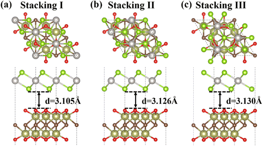 |
| | Fig. 2 Top and side views of three different stacking configurations of the PtSe2/Hf2CO2 heterostructure: (a) stacking I, (b) stacking II, (c) stacking III. | |
Table 1 Lattice parameter (a), bond length (Lx–x), band energy (Eg), interlayer distance (d) and binding energy (Eb)
| System |
Type |
a (Å) |
LPt–Se (Å) |
LHf–O (Å) |
LHf–C (Å) |
PBE/HSE06 Eg (eV) |
d (Å) |
Eb (meV Å−2) |
| PtSe2 |
— |
3.748 |
2.528 |
— |
— |
1.398/1.990 |
— |
— |
| Hf2CO2 |
— |
3.265 |
— |
2.100 |
2.335 |
0.988/1.749 |
— |
— |
| PtSe2/Hf2CO2 |
I |
6.492 |
2.529 |
2.096 |
2.324 |
0.965/1.788 |
3.105 |
−23.082 |
| II |
6.491 |
2.529 |
2.094 |
2.328 |
0.964/— |
3.126 |
−22.959 |
| III |
6.491 |
2.530 |
2.094 |
2.327 |
0.957/— |
3.130 |
−22.887 |
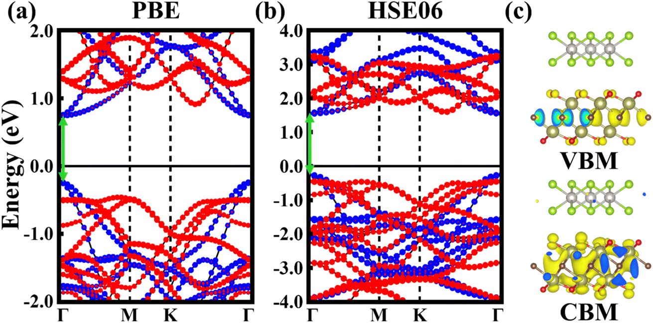
Fig. 3a and b show the band structures of the PtSe2/Hf2CO2 heterostructure with stacking I configuration, calculated by the PBE/HSE06 functional. Both the CBM and the VBM are contributed by Hf2CO2 layer. The band gap of the heterostructure is respectively 0.965/1.788 eV using PBE/HSE06 functional. Fig. 3c displays the band-resolved charge densities of the CBM and VBM for the PtSe2/Hf2CO2 vdW heterostructure. The results indicate that the PtSe2/Hf2CO2 vdW heterostructure exhibits a type-I band alignment. Besides, we found that the PBE functional has indeed underestimated the band gap value, but the band structure obtained from PBE has almost exhibited the same trend to that obtained from HSE06 functional.
 |
| | Fig. 3 (a) and (b) The projected band structures of PtSe2/Hf2CO2 heterostructure calculated by PBE and HSE06 method, respectively, the Fermi level is set as zero, the red and blue lines represent PtSe2 and Hf2CO2, respectively. (c) The partial charge densities corresponding to the VBM and CBM of the PtSe2/Hf2CO2 heterostructure. | |
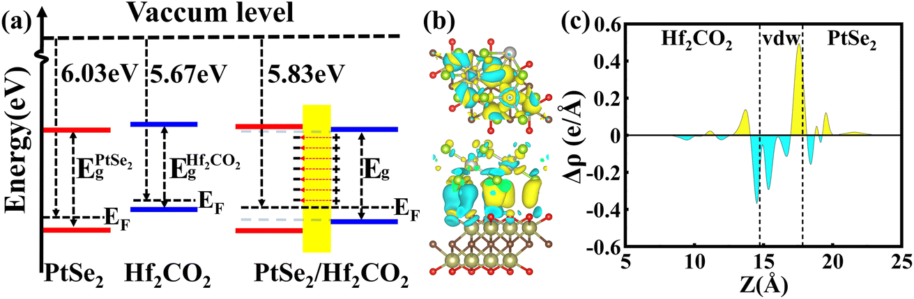
Next, the work function is employed to deeply understand the band alignment of the PtSe2/Hf2CO2 vdW heterostructure. The definition of work function (Φ) is
where
Evac and
EF represent the vacuum level and Fermi level, respectively. The calculated work function of the PtSe
2 layer and the Hf
2CO
2 layer are 6.03 and 5.67 eV, respectively, shown in
Table 2. The electrons move from Hf
2CO
2 layer to the PtSe
2 layer due to the smaller work function of Hf
2CO
2 layer, resulting in an electric field (
Ein) in the interlayer, which, in turn, impedes the transfer of charge and ultimately establishes an electrostatic equilibrium, as shown in
Fig. 4a. As a result of charge transfer, the Fermi level of the PtSe
2 layer moves up while the Fermi level of the Hf
2CO
2 layer goes down for equilibrium Fermi level. Consequently, the work function of the heterostructure is calculated to be 5.83 eV.
Table 2 Edges of VBM and CBM and work function for materials
| System |
VBM (eV) |
CBM (eV) |
Work function (eV) |
| Isolated |
PtSe2 |
−4.25 |
−6.24 |
6.03 |
| Hf2CO2 |
−4.28 |
−0.68 |
5.67 |
| PtSe2/Hf2CO2 |
PtSe2 |
−4.28 |
−6.08 |
5.83 |
| Hf2CO2 |
−4.23 |
−6.29 |
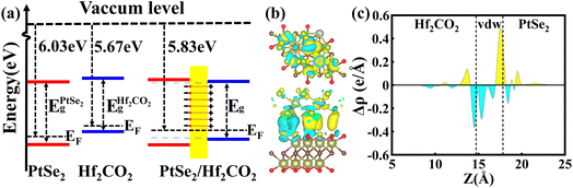 |
| | Fig. 4 (a) The band alignment of PtSe2/Hf2CO2 vdW heterostructure. , ,  and Eg are the band gaps of PtSe2 layer, Hf2CO2 layer and PtSe2/Hf2CO2 heterostructure, respectively. (b) The side and top views of the 3D isosurface with charge density difference for PtSe2/Hf2CO2 heterostructure. The cyan and yellow regions represent the electrons depletion and accumulation, respectively. The charge density value corresponding to the isosurfaces drawn is 0.805e Å−3. (c) The planar-averaged charge density difference for PtSe2/Hf2CO2 heterostructure. and Eg are the band gaps of PtSe2 layer, Hf2CO2 layer and PtSe2/Hf2CO2 heterostructure, respectively. (b) The side and top views of the 3D isosurface with charge density difference for PtSe2/Hf2CO2 heterostructure. The cyan and yellow regions represent the electrons depletion and accumulation, respectively. The charge density value corresponding to the isosurfaces drawn is 0.805e Å−3. (c) The planar-averaged charge density difference for PtSe2/Hf2CO2 heterostructure. | |
To visualize the charge transfer and charge redistribution, the differential charge density (Δρ) have been studied. The Δρ was determined as:
| | |
Δρ = ρPtSe2/Hf2CO2 − ρPtSe2 − ρHf2CO2
| (3) |
where
ρPtSe2/Hf2CO2,
ρPtSe2, and
ρHf2CO2 are the charge densities of the PtSe
2/Hf
2CO
2 heterostructure and isolated PtSe
2 and Hf
2CO
2 monolayers, respectively. The 3D charge density difference is depicted in
Fig. 4b, with the cyan area signifying electron gain and the yellow area signifying electron loss. The electrons and holes are located on the PtSe
2 layer and Hf
2CO
2 layer, respectively. The planar-averaged differential charge density is described in
Fig. 4c. Positive and negative values reflect charge accumulation and depletion, respectively. At the surface of PtSe
2/Hf
2CO
2 heterostructure, electrons acculmulated on the PtSe
2 side and depleted on the Hf
2CO
2 side, indicating electron transfer from the Hf
2CO
2 layer to the PtSe
2 layer after the two layers contact.
3.3. Effect of external electric field
In order to explore the possible application of the PtSe2/Hf2CO2 vdW heterostructure, we have modulated the electronic properties by applying external electric field. Considering that although the PBE functional underestimates the bandgap, it is still able to predict the correct trend in bandgap variation and to properly demonstrate the physical mechanisms. Therefore, we adopted the PBE functional in the following calculations due to the high computational cost of HSE06.
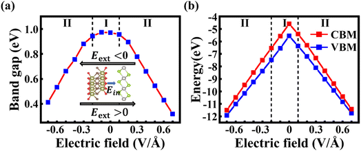
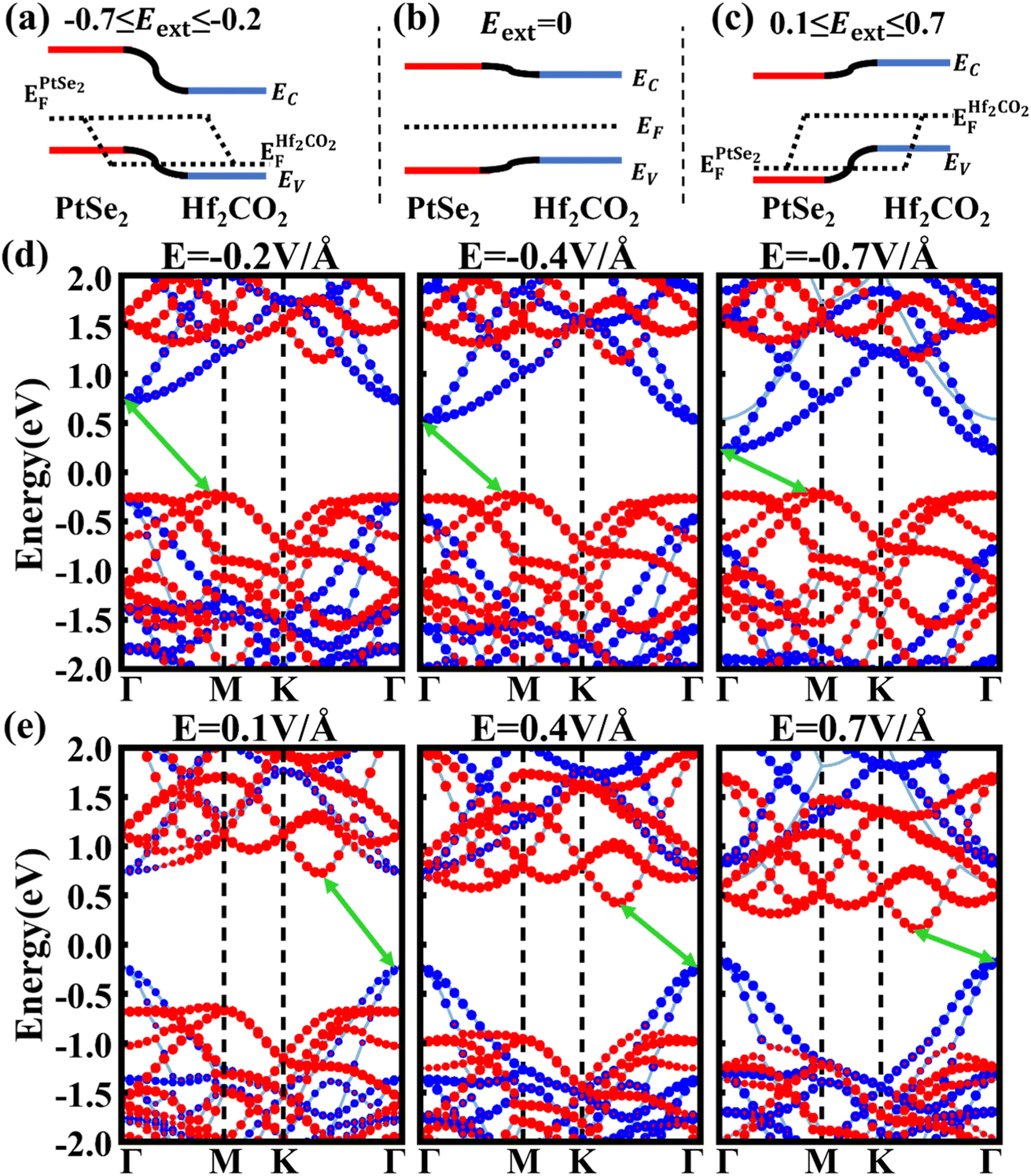
The direction of Eext from the Hf2CO2 layer to the PtSe2 layer is taken as the positive direction (shown in Fig. 5a) and the Eext ranging from −0.7 to 0.7 V Å−1 is applied. Fig. 5a and b show the band gap and band edges (VBM, CBM) as a function of the applied electric field. When the negative Eext is applied, a transition from type-I to type-II occurs at −0.2 V Å−1, and the band gap value decreases linearly with increasing the negative electric field. In the type-II heterostructure induced by negative electric field, the CBM and VBM are dominated by PtSe2 and Hf2CO2 layers, respectively, as shown in Fig. 6d. Under the influence of the positive Eext, the transition from type-I to type-II takes place at 0.1 V Å−1. However, in contrast to the case of the negative electric field, the CBM and VBM of the type-II heterostructure are dominated by Hf2CO2 and PtSe2, respectively, as shown in Fig. 6e. And the band gap value decreases linearly with increasing the positive electric field. The linear variations of band gaps with Eext can be attributed to the Stark effect.55
 |
| | Fig. 5 (a) The band gap evolution of PtSe2/Hf2CO2 heterostructure as a function of Eext. The inset shows directions of build-in electric field, negative and positive external electric field. (b) The band edge evolution of PtSe2/Hf2CO2 heterostructure as a function of Eext. | |
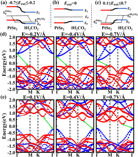 |
| | Fig. 6 (a) Type-II band alignment under a negative external electric field. (b) Type-I band alignment without an external electric field, and (c) Type-II band alignment under a positive external electric field.  and and  are the quasi-Fermi levels of PtSe2 and Hf2CO2 layers in the heterostructure, respectively. (d), (e) The band structures of PtSe2/Hf2CO2 heterostructure under the negative of −0.2, −0.4 and −0.7 V Å−1, and positive electric fields of 0.1, 0.4 and 0.7 V Å−1, respectively, where the red and blue dots represent PtSe2 and Hf2CO2, respectively. The green arrow lines denote the CBM and VBM. are the quasi-Fermi levels of PtSe2 and Hf2CO2 layers in the heterostructure, respectively. (d), (e) The band structures of PtSe2/Hf2CO2 heterostructure under the negative of −0.2, −0.4 and −0.7 V Å−1, and positive electric fields of 0.1, 0.4 and 0.7 V Å−1, respectively, where the red and blue dots represent PtSe2 and Hf2CO2, respectively. The green arrow lines denote the CBM and VBM. | |
When applying a negative Eext, the total electric field is weakened due to the opposite direction of the built-in and external electric field. In this case, the drift of electrons from the Hf2CO2 layer to the PtSe2 layer is further strengthened, resulting in a downward shift of the quasi-Fermi level of the Hf2CO2 layer and an upward shift of the quasi-Fermi level of the PtSe2 layer, shown in Fig. 6a. As shown in Fig. 6c, when the positive Eext is applied, the built-in electric field and external electric field have the same direction, and the total electric field is enhanced, causing an upward of  and a downward of
  . The response of the electrical properties of PtSe2/Hf2CO2 heterostructure to Eext makes the PtSe2/Hf2CO2 heterostructure exhibit potential applications in FETs and MEMS.
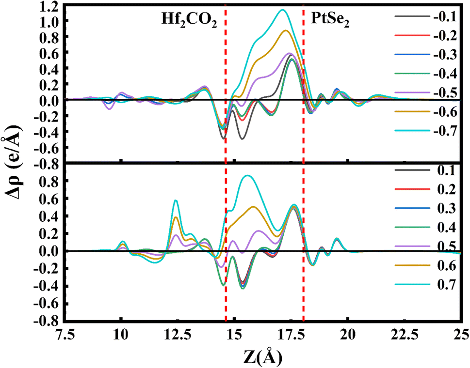
The distinct responses of the electronic properties of PtSe2/Hf2CO2 heterostructure to positive and negative electric fields can be attributed to the charge transfer and redistribution between the PtSe2 and Hf2CO2 layers. Therefore, the planar-average charge density difference of heterostructure under different Eext is plotted in Fig. 7. The positive and negative values reflect electrons accumulation and depletion, respectively. It can be obviously seen that the number of accumulated electrons at the PtSe2 side increases with the enhanced strength of the negative Eext, while the number of depleted electrons near the Hf2CO2 surface decreases with the positive Eext increasing from 0.1 to 0.4 V Å−1, then the electrons accumulation occurs at Eext = 0.5 V Å−1, and the number of accumulated electrons increases with the enhanced strength of the positive Eext.
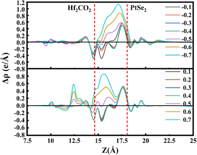 |
| | Fig. 7 The planar-averaged difference charge density of the PtSe2/Hf2CO2 heterostructure with various Eext. | |
3.4. Effect of biaxial strain
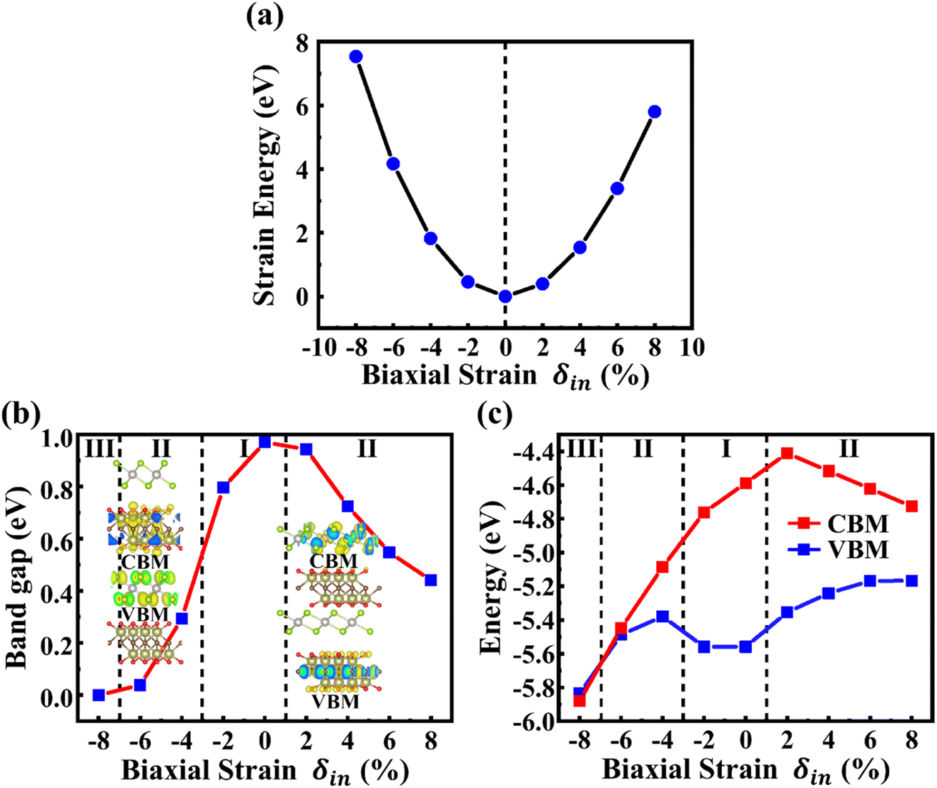
Biaxial strain has also been regarded as a powerful tool for tuning the electronic properties of 2D materials and vdW heterostructures. In this work, the electronic properties of PtSe2/Hf2CO2 heterostructures have been investigated under a series of biaxial strains ranging from −8% to 8%, with a step of 2%. Fig. 8a depicts the strain energy (ES), checked by ES = E1 − E0, in which E1 and E0 are its total energies of strained and original structures with no strain applied, respectively. The ES increases quadratically with strain, indicating that all strains studied are below the elastic limit and are therefore fully reversible.54,56
 |
| | Fig. 8 (a) Strain energies at various biaxial strains ranging from −8% to 8%. (b) and (c) The band gap and band edge evolution of PtSe2/Hf2CO2 heterostructure as a function of biaxial strains. | |
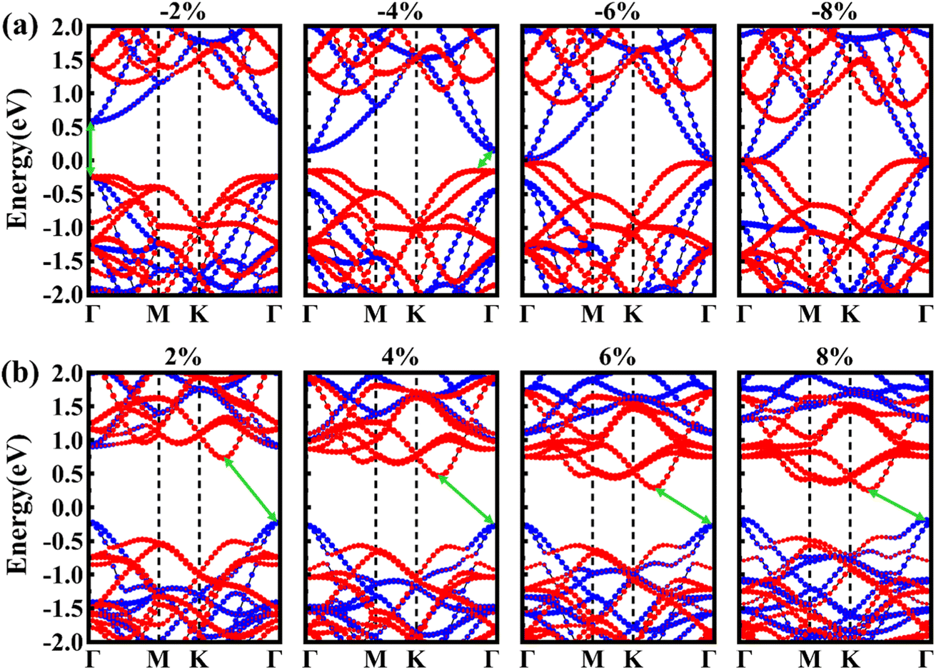
Fig. 8b and c illustrate the evolution of the bandgap and the band edges (CBM and VBM) of PtSe2/Hf2CO2 heterostructure as a function of the strain. The two inset plots illustrate the two different type-II band alignments. One can see that the band gap of PtSe2/Hf2CO2 heterostructure decreases with increasing the compressive strain. When the compressive strain is increased to −4%, a type-I to type-II band alignment transition takes place, and the CBM and VBM are contributed by Hf2CO2 layer and PtSe2 layer, respectively, then a semiconductor-to-metal transition occurs when the compressive strain is increased to −8%. On the contrary, the PtSe2/Hf2CO2 heterostructure is transformed to a type-II heterostructure when the PtSe2/Hf2CO2 heterostructure is increase to 2%, in which the CBM and VBM are located in PtSe2 layer and Hf2CO2 layer, respectively. To further unravel the modulation mechanism of strain effects on electronic properties of PtSe2/Hf2CO2 heterostructure, the electronic band structures under different strains are plotted in Fig. 9. After application of −2% compressive strain, the VBM of PtSe2 layer increases, closing to the VBM of Hf2CO2 layer. When the compressive strain is increased to −4%, the VBM of PtSe2 layer continue to increase, higher than the VBM of Hf2CO2 layer, resulting in a type-I to type-II transition. With the compressive strain increased to −8%, the VBM of PtSe2 layer is higher than the CBM of Hf2CO2 layer, a semiconductor-to-metal occurs. Besides, we found that the band gap of PtSe2 layer increases then decreases while the band gap of Hf2CO2 layers decreases with increasing the compressive strain. For the tensile strain, the CBM of Hf2CO2 layer greatly increases at the strain of −2%, thus changes the CBM of the heterostructure from Hf2CO2 to PtSe2 layer. As a result, a type-I to type-II transition takes place. With the increase of the tensible strain, the CBM of PtSe2 layer decreases, inducing the decrease of the bandgap of PtSe2/Hf2CO2 heterostructure. In addition, we found that the bandgap of Hf2CO2 layers increases while the bandgap of PtSe2 layers decreases with increasing the tensible strain.
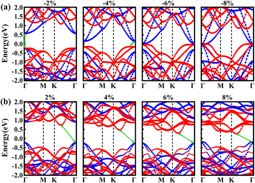 |
| | Fig. 9 (a) The electronic band structures of PtSe2/Hf2CO2 heterostructure under compressive strains in the range of −2% to 8%. (b) The electronic band structures of PtSe2/Hf2CO2 heterostructure under tensile strains in the range of 2% to 8%. The red circles represent the band of PtSe2 layer, and the blue circles represent the band of Hf2CO2 layer. | |
4. Conclusions
In this work, the structural and electronic properties of PtSe2/Hf2CO2 heterostructures have been systematically investigated using first principles calculations. The PtSe2/Hf2CO2 bilayer forms a stable vdW heterostructure. In equilibrium PtSe2/Hf2CO2 heterostructures, both the CBM and VBM are donated by the Hf2CO2 layer, resulting in a type-I band alignment, which can be utilized in LEDs or other optoelectronic devices. It has been also demonstrated that the electronic properties of PtSe2/Hf2CO2 vdW heterostructure are insensitive to diverse stacking patterns whereas external electric field and biaxial strain have been proved to be efficient methods for modulating the electrical properties of PtSe2/Hf2CO2 heterostructure. Both the external electric field and biaxial strain can induce type-I to type-II band alignment transition, which facilitate the separation of photoexcited electrons and holes, enabling high efficiency optoelectronics and solar energy conversion. Furthermore, the band gap of PtSe2/Hf2CO2 heterostructure decreases with increasing the strength of external electric field or biaxial strain after the occurrence of type-I to type-II transition. In addition, a semiconductor-to-metal transition takes place under the strong compressive strain of −8%. According to our results, the PtSe2/Hf2CO2 heterostructure will present abundant opportunities for the application of flexible electronic and optoelectronic nano-devices.
Conflicts of interest
There are no conflicts to declare.
References
- Q. H. Wang, K. Kalantar-Zadeh, A. Kis, J. N. Coleman and M. S. Strano, Electronics and optoelectronics of two-dimensional transition metal dichalcogenides, Nat. Nanotechnol., 2012, 7, 699–712 CrossRef CAS PubMed.
- K. Tran, G. Moody, F. Wu, X. Lu, J. Choi, K. Kim, A. Rai, D. A. Sanchez, J. Quan and A. Singh, Evidence for moiré excitons in van der Waals heterostructures, Nature, 2019, 567, 71–75 CrossRef CAS PubMed.
- T. Musso, P. V. Kumar, A. S. Foster and J. C. Grossman, Graphene oxide as a promising hole injection layer for MoS2-based electronic devices, ACS Nano, 2014, 8, 11432–11439 CrossRef CAS PubMed.
- K. Kośmider and J. Fernández-Rossier, Electronic properties of the MoS2-WS2 heterojunction, Phys. Rev. B: Condens. Matter Mater. Phys., 2013, 87, 075451 CrossRef.
- Y. He, Y. Yang, Z. Zhang, Y. Gong, W. Zhou, Z. Hu, G. Ye, X. Zhang, E. Bianco and S. Lei, Strain-induced electronic structure changes in stacked van der Waals heterostructures, Nano Lett., 2016, 16, 3314–3320 CrossRef CAS PubMed.
- X.-H. Li, X.-H. Cui, C.-H. Xing, H.-L. Cui and R.-Z. Zhang, Strain-tunable electronic and optical properties of Zr2CO2 MXene and MoSe2 van der Waals heterojunction: a first principles calculation, Appl. Surf. Sci., 2021, 548, 149249 CrossRef CAS.
- C.-H. Lee, G.-H. Lee, A. M. Van Der Zande, W. Chen, Y. Li, M. Han, X. Cui, G. Arefe, C. Nuckolls and T. F. Heinz, Atomically thin p–n junctions with van der Waals heterointerfaces, Nat. Nanotechnol., 2014, 9, 676–681 CrossRef CAS PubMed.
- L. Britnell, R. Gorbachev, R. Jalil, B. Belle, F. Schedin, A. Mishchenko, T. Georgiou, M. Katsnelson, L. Eaves and S. Morozov, Field-effect tunneling transistor based on vertical graphene heterostructures, Science, 2012, 335, 947–950 CrossRef CAS PubMed.
- J. Low, J. Yu, M. Jaroniec, S. Wageh and A. A. Al-Ghamdi, Heterojunction photocatalysts, Adv. Mater., 2017, 29, 1601694 CrossRef PubMed.
- Z. Lu, D. Lockwood and J.-M. Baribeau, Quantum confinement and light emission in SiO2/Si superlattices, Nature, 1995, 378, 258–260 CrossRef CAS.
- Z. Guo, N. Miao, J. Zhou, B. Sa and Z. Sun, Strain-mediated type-I/type-II transition in MXene/Blue phosphorene van der Waals heterostructures for flexible optical/electronic devices, J. Mater. Chem. C, 2017, 5, 978–984 RSC.
- R. Marschall, Semiconductor composites: strategies for enhancing charge carrier separation to improve photocatalytic activity, Adv. Funct. Mater., 2014, 24, 2421–2440 CrossRef CAS.
- G. Wang, L. Gong, Z. Li, B. Wang, W. Zhang, B. Yuan, T. Zhou, X. Long and A. Kuang, A two-dimensional CdO/CdS heterostructure used for visible light photocatalysis, Phys. Chem. Chem. Phys., 2020, 22, 9587–9592 RSC.
- J. Na, Y. Kim, J. H. Smet, M. Burghard and K. Kern, Gate-tunable tunneling transistor based on a thin black phosphorus–SnSe2 heterostructure, ACS Appl. Mater. Interfaces, 2019, 11, 20973–20978 CrossRef CAS PubMed.
- C. Tan, S. Yin, J. Chen, Y. Lu, W. Wei, H. Du, K. Liu, F. Wang, T. Zhai and L. Li, Broken-gap PtS2/WSe2 van der Waals heterojunction with ultrahigh reverse rectification and fast photoresponse, ACS Nano, 2021, 15, 8328–8337 CrossRef CAS PubMed.
- X. Cong, Y. Zheng, F. Huang, Q. You, J. Tang, F. Fang, K. Jiang, C. Han and Y. Shi, Efficiently band-tailored type-III van der Waals heterostructure for tunnel diodes and optoelectronic devices, Nano Res., 2022, 15, 8442–8450 CrossRef CAS.
- H. V. Phuc, N. N. Hieu, B. D. Hoi and C. V. Nguyen, Interlayer coupling and electric field tunable electronic properties and Schottky barrier in a graphene/bilayer-GaSe van der Waals heterostructure, Phys. Chem. Chem. Phys., 2018, 20, 17899–17908 RSC.
- K. Rahimi, Electric-field-and strain-induced adjustability of vdW heterostructure of g-ZnO/2H-TiS2 for optoelectronic applications, Mater. Lett., 2021, 282, 128680 CrossRef CAS.
- W. Guo, X. Ge, S. Sun, Y. Xie and X. Ye, The strain effect on the electronic properties of the MoSSe/WSSe van der Waals heterostructure: a first-principles study, Phys. Chem. Chem. Phys., 2020, 22, 4946–4956 RSC.
- M. Naguib, M. Kurtoglu, V. Presser, J. Lu, J. Niu, M. Heon, L. Hultman, Y. Gogotsi and M. W. Barsoum, Two-dimensional nanocrystals produced by exfoliation of Ti3AlC2, Adv. Mater., 2011, 23, 4248–4253 CrossRef CAS PubMed.
- R. Ma, Z. Chen, D. Zhao, X. Zhang, J. Zhuo, Y. Yin, X. Wang, G. Yang and F. Yi, Ti3C2TxMXene for electrode materials of supercapacitors, J. Mater. Chem. A, 2021, 9, 11501–11529 RSC.
- O. Folorunso, N. Kumar, Y. Hamam, R. Sadiku and S. S. Ray, Recent progress on 2D metal carbide/nitride (MXene) nanocomposites for lithium-based batteries, FlatChem, 2021, 29, 100281 CrossRef CAS.
- S. Venkateshalu and A. N. Grace, MXenes—a new class of 2D layered materials: synthesis, properties, applications as supercapacitor electrode and beyond, Appl. Mater. Today, 2020, 18, 100509 CrossRef.
- S.-C. Zhu, S. Li, B. Tang, H. Liang, B.-J. Liu, G. Xiao and F.-X. Xiao, MXene-motivated accelerated charge transfer over TMCs quantum dots for solar-powered photoreduction catalysis, J. Catal., 2021, 404, 56–66 CrossRef CAS.
- J. Nan, X. Guo, J. Xiao, X. Li, W. Chen, W. Wu, H. Liu, Y. Wang, M. Wu and G. Wang, Nanoengineering of 2D MXene-based materials for energy storage applications, Small, 2021, 17, 1902085 CrossRef CAS PubMed.
- H. Zhang, G. Yang, X. Zuo, H. Tang, Q. Yang and G. Li, Computational studies on the structural, electronic and optical properties of graphene-like MXenes (M2CT2, M = Ti, Zr, Hf; T = O, F, OH) and their potential applications as visible-light driven photocatalysts, J. Mater. Chem. A, 2016, 4, 12913–12920 RSC.
- X.-H. Zha, Q. Huang, J. He, H. He, J. Zhai, J. S. Francisco and S. Du, The thermal and electrical properties of the promising semiconductor MXene Hf2CO2, Sci. Rep., 2016, 6, 27971 CrossRef PubMed.
- X. Li, Y. Dai, Y. Ma, Q. Liu and B. Huang, Intriguing electronic properties of two-dimensional MoS2/TM2CO2 (TM = Ti, Zr, or Hf) hetero-bilayers: type-II semiconductors with tunable band gaps, Nanotechnology, 2015, 26, 135703 CrossRef PubMed.
- Y. Zhang, R. Xiong, B. Sa, J. Zhou and Z. Sun, MXenes: promising donor and acceptor materials for high-efficiency heterostructure solar cells, Sustainable Energy Fuels, 2021, 5, 135–143 RSC.
- L. Li, H.-T. Yan and X.-H. Li, Effect of preadsorbing gas molecules on the adsorption of SO2 molecule on Hf2CO2 MXene by first-principles study, Surf. Interfaces, 2023, 102639 CrossRef CAS.
- J. Hao, J. Wu, D. Wang, C. Wang, M. Luo, L. Xie, F. Zhu, X. Yan and Y. Gu, Highly efficient photocatalytic overall water splitting in two-dimensional van der Waals MoS2/Hf2CO2 heterostructure, J. Phys. D: Appl. Phys., 2022, 56, 035501 CrossRef.
- B. Zhu, F. Zhang, J. Qiu, X. Chen, K. Zheng, H. Guo, J. Yu and J. Bao, A novel Hf2CO2/WS2 van der Waals heterostructure as a potential candidate for overall water splitting photocatalyst, Mater. Sci. Semicond. Process., 2021, 133, 105947 CrossRef CAS.
- M. Zhang, R. Si, X. Wu, Y. Dong, K. Fu, X. Xu, J. Zhang, L. Li and Y. Guo, Two-dimensional Hf2CO2/GaN van der Waals heterostructure for overall water splitting: a density functional theory study, J. Mater. Sci.: Mater. Electron., 2021, 32, 19368–19379 CrossRef CAS.
- A. Kandemir, B. Akbali, Z. Kahraman, S. Badalov, M. Ozcan, F. İyikanat and H. Sahin, Structural, electronic and phononic properties of PtSe2: from monolayer to bulk, Semicond. Sci. Technol., 2018, 33, 085002 CrossRef.
- K. Ullah, S. Ye, S.-B. Jo, L. Zhu, K.-Y. Cho and W.-C. Oh, Optical and photocatalytic properties of novel heterogeneous PtSe2–graphene/TiO2 nanocomposites synthesized via ultrasonic assisted techniques, Ultrason. Sonochem., 2014, 21, 1849–1857 CrossRef CAS PubMed.
- X. Zhao, W. Niu, H. Zhang, X. Dai, S. Wei and L. Yang, Effects of interlayer coupling and electric field on the electronic properties of PtSe2/ZrSe2 van der Waals heterojunctions, Appl. Surf. Sci., 2020, 510, 145316 CrossRef CAS.
- P. Li, L. Li and X. C. Zeng, Tuning the electronic properties of monolayer and bilayer PtSe2 via strain engineering, J. Mater. Chem. C, 2016, 4, 3106–3112 RSC.
- C. Yim, K. Lee, N. McEvoy, M. O'Brien, S. Riazimehr, N. C. Berner, C. P. Cullen, J. Kotakoski, J. C. Meyer and M. C. Lemme, High-performance hybrid electronic devices from layered PtSe2 films grown at low temperature, ACS Nano, 2016, 10, 9550–9558 CrossRef CAS PubMed.
- Z. Wang, Q. Li, F. Besenbacher and M. Dong, Facile synthesis of single crystal PtSe2 nanosheets for nanoscale electronics, Adv. Mater., 2016, 28, 10224–10229 CrossRef CAS PubMed.
- K. Ullah, S. Ye, L. Zhu, S. B. Jo, W. K. Jang, K.-Y. Cho and W.-C. Oh, Noble metal doped graphene nanocomposites and its study of photocatalytic hydrogen evolution, Solid State Sci., 2014, 31, 91–98 CrossRef CAS.
- M. Sajjad, E. M. Muñoz, N. Singh and U. Schwingenschlögl, Superior gas sensing properties of monolayer PtSe2, Adv. Mater. Interfaces, 2016, 4, 1600911 CrossRef.
- J. Hafner, Ab-initio simulations of materials using VASP: density-functional theory and beyond, J. Comput. Chem., 2008, 29, 2044–2078 CrossRef CAS PubMed.
- G. Kresse and J. Furthmüller, Efficient iterative schemes for ab initio total-energy calculations using a plane-wave basis set, Phys. Rev. B: Condens. Matter Mater. Phys., 1996, 54, 11169 CrossRef CAS PubMed.
- J. P. Perdew, K. Burke and M. Ernzerhof, Generalized gradient approximation made simple, Phys. Rev. Lett., 1996, 77, 3865 CrossRef CAS PubMed.
- S. Grimme, J. Antony, S. Ehrlich and H. Krieg, A consistent and accurate ab initio parametrization of density functional dispersion correction (DFT-D) for the 94 elements H-Pu, J. Chem. Phys., 2010, 132, 154104 CrossRef PubMed.
- S. Han, Y. Li and Z. Wang, PtSe2/SiH van der Waals type-II heterostructure: a high efficiency photocatalyst for water splitting, Phys. Chem. Chem. Phys., 2020, 22, 17145–17151 RSC.
- R. Momeni Feili, M. Dadsetani, R. Nejatipour and A. Ebrahimian, Electron Energy Loss Structures of Terminated Scandium and Hafnium MXene Monolayers from First-Principles
Calculations, J. Electron. Mater., 2020, 49, 2502–2520 CrossRef CAS.
- X. Meng, Y. Shen, J. Liu, L. Lv, X. Yang, X. Gao, M. Zhou, X. Wang, Y. Zheng and Z. Zhou, The PtSe2/GaN van der Waals heterostructure photocatalyst with type II alignment: a first-principles study, Appl. Catal., A, 2021, 624, 118332 CrossRef CAS.
- K. Ren, W. Tang, M. Sun, Y. Cai, Y. Cheng and G. Zhang, A direct Z-scheme PtS2/arsenene van der Waals heterostructure with high photocatalytic water splitting efficiency, Nanoscale, 2020, 12, 17281–17289 RSC.
- C. Fu, G. Wang, Y. Huang, Y. Chen, H. Yuan, Y. S. Ang and H. Chen, Two-dimensional CdS/SnS2 heterostructure: a highly efficient direct Z-scheme water splitting photocatalyst, Phys. Chem. Chem. Phys., 2022, 24, 3826–3833 RSC.
- G. Wang, F. Zhou, B. Yuan, S. Xiao, A. Kuang, M. Zhong, S. Dang, X. Long and W. Zhang, Strain-Tunable Visible-Light-Responsive Photocatalytic Properties of Two-Dimensional CdS/g-C(3)N(4): A Hybrid Density Functional Study, Nanomaterials, 2019, 9, 244 CrossRef CAS PubMed.
- F. Opoku, A. Aniagyei, O. Akoto, E. E. Kwaansa-Ansah, N. K. Asare-Donkor and A. A. Adimado, Effect of van der Waals stacking in CdS monolayer on enhancing the hydrogen production efficiency of SiH monolayer, Mater. Adv., 2022, 3, 4629–4640 RSC.
- Y. Fan, B. Yang, X. Song, X. Shao and M. Zhao, Direct Z-scheme photocatalytic overall water splitting on 2D CdS/InSe heterostructures, J. Phys. D: Appl. Phys., 2018, 51, 395501 CrossRef.
- L. Fang, Y. Ni, J. Hu, Z. Tong, X. Ma, H. Lv and S. Hou, First-principles insights of electronic properties of Blue Phosphorus/MoSi2N4 van der Waals heterostructure via vertical electric field and biaxial strain, Phys. E, 2022, 143, 115321 CrossRef CAS.
- F. Zheng, Z. Liu, J. Wu, W. Duan and B.-L. Gu, Scaling law of the giant Stark effect in boron nitride nanoribbons and nanotubes, Phys. Rev. B: Condens. Matter Mater. Phys., 2008, 78, 085423 CrossRef.
- J. Wang, Y. Huang, F. Ma, J. Zhang, X. Wei and J. Liu, Strain engineering the electronic and photocatalytic properties of WS2/blue phosphene van der Waals heterostructures, Catal. Sci. Technol., 2021, 11, 179–190 RSC.
Footnote |
| † Electronic supplementary information (ESI) available. For ESI and crystallographic data in CIF or other electronic format see DOI: https://doi.org/10.1039/d3ra04363k |
|
| This journal is © The Royal Society of Chemistry 2023 |
Click here to see how this site uses Cookies. View our privacy policy here. 
 Open Access Article
 This Open Access Article is licensed under a Creative Commons Attribution-Non Commercial 3.0 Unported Licence
 ,
Yi Peng,
Li Fang
,
Yi Peng,
Li Fang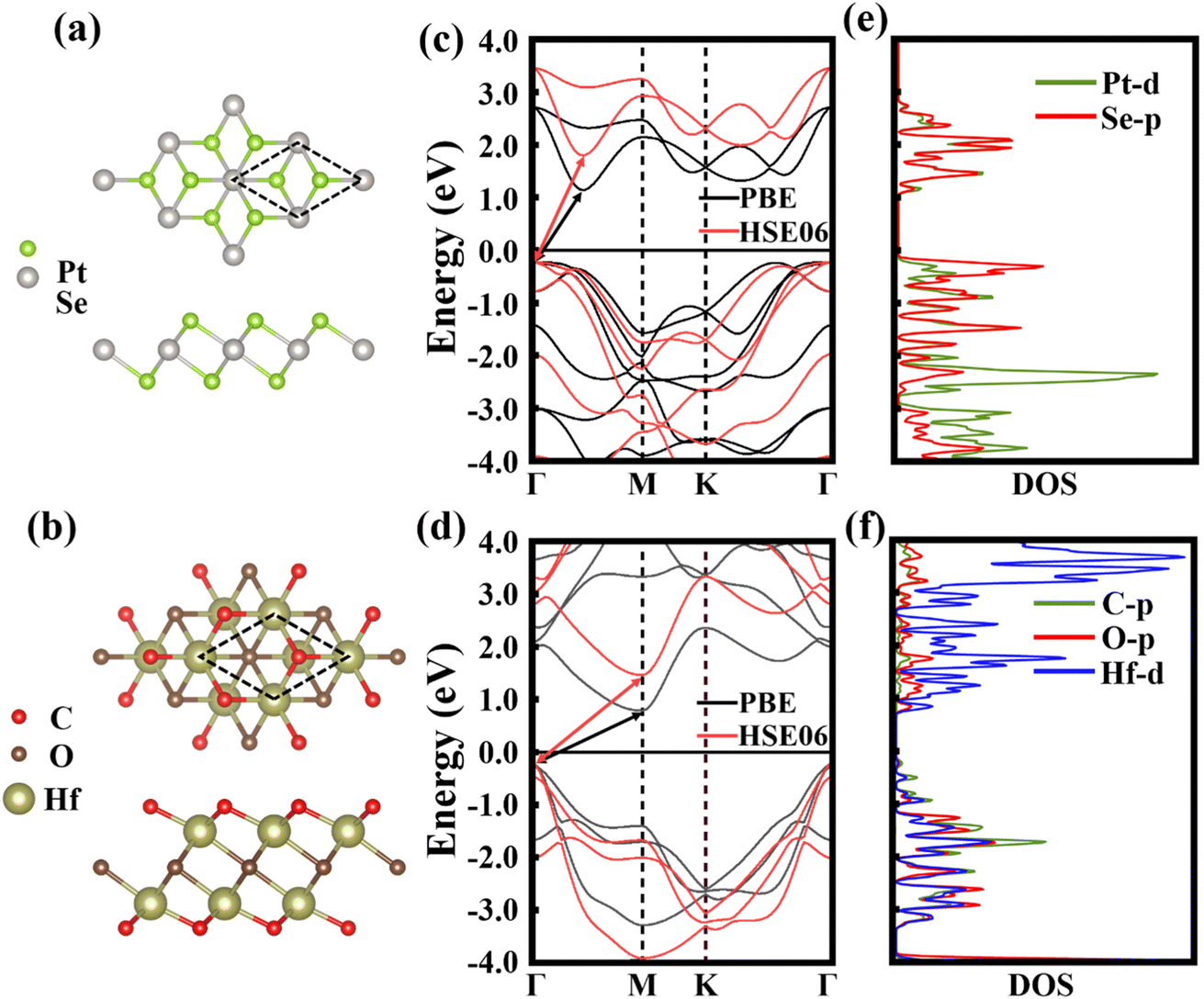
 supercell of PtSe2 and 2 × 2 supercell of Hf2CO2 are used to construct the PtSe2/Hf2CO2 heterostructure. The lattice mismatch is only 0.29%, making it more possible to achieve experimental synthesis of the PtSe2/Hf2CO2 heterostructure. In Fig. 2, three distinct stacking configurations of PtSe2/Hf2CO2 heterostructure were studied. These configurations were created by shifting the relative positions of two layers in the horizontal direction. The binding energy Eb were calculated to estimate the thermodynamic stability of the system. It is defined as follows:
 ,
,  and Eg are the band gaps of PtSe2 layer, Hf2CO2 layer and PtSe2/Hf2CO2 heterostructure, respectively. (b) The side and top views of the 3D isosurface with charge density difference for PtSe2/Hf2CO2 heterostructure. The cyan and yellow regions represent the electrons depletion and accumulation, respectively. The charge density value corresponding to the isosurfaces drawn is 0.805e Å−3. (c) The planar-averaged charge density difference for PtSe2/Hf2CO2 heterostructure.
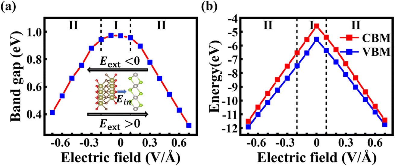
 and
and  are the quasi-Fermi levels of PtSe2 and Hf2CO2 layers in the heterostructure, respectively. (d), (e) The band structures of PtSe2/Hf2CO2 heterostructure under the negative of −0.2, −0.4 and −0.7 V Å−1, and positive electric fields of 0.1, 0.4 and 0.7 V Å−1, respectively, where the red and blue dots represent PtSe2 and Hf2CO2, respectively. The green arrow lines denote the CBM and VBM.
 and a downward of
  . The response of the electrical properties of PtSe2/Hf2CO2 heterostructure to Eext makes the PtSe2/Hf2CO2 heterostructure exhibit potential applications in FETs and MEMS.