DOI:
10.1039/D3RA03956K
(Paper)
RSC Adv., 2023,
13, 21882-21889
Bulk synthesis of conductive non-metallic carbon nanospheres and a 3D printed carrier device for scanning electron microscope calibration†
Received
13th June 2023
, Accepted 12th July 2023
First published on 19th July 2023
Abstract
Herein, a facile method is proposed for the bulk synthesis of conductive non-metallic carbon nanospheres with controllable morphology to replace conventional metal calibration reference materials (CRMs), such as gold nanoparticles and copper grids. The prepared nanospheres had an average diameter of ∼222 ± 23 nm, where silicon dioxide formed the core and the shell was comprised of the carbon layer. The structure of the conductive carbon nanospheres was characterized using FTIR, SEM, EDS and TEM. Additionally, an innovative design was demonstrated by 3D printing the calibration carrier device. Furthermore, the stability and image linear distortion of the conductive carbon nanospheres were verified using analysis of variance (ANOVA). The results demonstrated that the accelerating voltage, magnification, and various positions in the X/Y axes had no significant effect on measured diameter of nanospheres, which was evident from all the p values being greater than 0.05. The comprehensive set of results reveal that conductive carbon nanospheres have great potential to replace traditional CRMs.
1. Introduction
Scanning electron microscopy (SEM) has been widely used for materials characterization across several fields such as life science, materials science, and microelectronics as it offers advantages such as continuously adjustable magnification, high resolution and extended depth of field.1–3 Since SEM utilizes electron beams for progressive scanning, problems such as image magnification and distortion can occur over extended operational times. In order to maintain a stable mode of operation that can give high-quality images and measurement data, regular calibration is necessary using calibration reference materials (CRMs).4,5
According to the National Institute of Standards and Technology (NIST, USA), gold nanoparticles, lithographically patterned silicon chips and copper grids are some of the commercially available CRMs that are commonly used today.6 However, the manufacturing process for these CRMs is typically demanding, highly costly, and requires specialized storage conditions. Additionally, they are more significantly affected by the environment (such as temperature and humidity) stemming from their own metal material.7 After repeated use at different environments, we cannot distinguish whether the difference between the measured true value and the standard value comes from CRMs or from the SEM equipment. Above all, the current CRMs cannot be prepared on a large scale in the laboratory. Therefore, it is particularly important to design and synthesize a reference non-metallic material at the laboratory level that has the same calibration as current CRMs, but are inexpensive, readily available and can be stored under regular conditions.
In this regard, hollow carbon spheres (HCS) have shown to possess excellent electrical conductivity and can fulfill the requirements of CRMs.8–14 However, CRMs also need to have a high level of mechanical strength. Hence, a material like silicon dioxide (SiO2) that has superior mechanical strength with controlled uniform spherical morphology can be used as the core material for HCS to enhance its mechanical strength.15–20 Therefore, the synthesis of conductive carbon-coated SiO2 nanospheres via a proper design strategy can fulfill the requirements of both conductivity and mechanical strength. Notably, there have been no reports on the use of carbon nanospheres for SEM calibration.
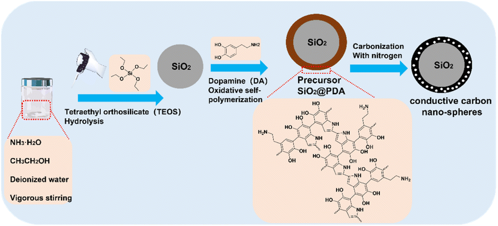
It is known that marine organisms, such as mussels, can attach to the surface of ships, reefs and other organisms by secreting strong adhesive Mytilus edulis foot proteins (Mefps), while Mefps contain a large number of catechol functional groups. Interestingly, dopamine (DA) has a molecular structure similar to Mefps and forms polydopamine (PDA) layers through covalent oxidative self-polymerization and non-covalent π–π stacking. It is the high catechol content of PDA that gives it strong interfacial adhesion properties and allows it to adhere to almost all types of organic and inorganic material surfaces.21–23 Herein, the synthesis approach is based on this phenomenon. Nanospheres of SiO2 can be prepared by a modified Stöber method.24–26 The oxidation-self-polymerization of PDA needs to be carried out under alkaline conditions,27–30 which coincides with the alkaline micro-environment of the synthesized SiO2 to further form a dense PDA layer on the SiO2 surface. Then the conductive carbon nanospheres are obtained by thermal cracking.
In this work, firstly, precursor PDA-coated SiO2 nanospheres (SiO2@PDA) are prepared by a one-step method. Secondly, conducting carbon nanospheres are prepared in bulk in the laboratory through the thermal decomposition of PDA. Finally, the prepared carbon nanospheres are used in the routine calibration of SEM, focusing on maintaining the stability and minimizing linear distortions in the image. In addition, the structural characterization of conducting carbon nanospheres is performed using Fourier transform infrared spectroscopy (FTIR), SEM, energy dispersive spectrometry (EDS) and transmission electron microscopy (TEM). Furthermore, the prepared conductive carbon nanospheres are also used for obtaining the particle size statistics to ascertain the presence any errors under different magnifications and accelerating voltages, and the corresponding error analysis is performed.
2. Experimental
2.1 Reagents and raw materials
The following reagents and raw materials were used in the synthesis: anhydrous ethanol (CH3CH2OH, AR, 99.5%), tetraethyl orthosilicate (C8H20O4Si, TEOS, AR), ammonia (NH3·H2O, AR, 25%) and dopamine (C8H11NO2, AR) were purchased from Shanghai Aladdin Bio-Chem Technology Co., Ltd, China. In addition, nitrogen (high purity, 99.999%) was obtained from Chengdu Kelong Chemical Co., Ltd, China.
2.2 Preparation of conductive carbon nanospheres
As shown in Fig. 1, first, 1 ml of 25% ammonia, 12 ml of 99.5% anhydrous ethanol and 80 ml of deionized water were measured and stirred vigorously for 30 min, while 1 ml of tetraethoxysilane (TEOS) was added dropwise and stirred vigorously for another 30 min. Next, 8 ml of 50 mg ml−1 of dopamine was added and stirred for 24 h for oxidation-self-polymerization, and the dark brown precursor polydopamine-coated SiO2 nanospheres (SiO2@PDA) were obtained after extraction. Eventually, the SiO2@PDA sample was dried in an oven for 12 h and then carbonized under the protection of nitrogen atmosphere using a programmable heating tube furnace. The heating rate of the furnace was 5 °C min−1, the rising temperature was 800 °C, and the holding time was 120 min. The final product was ground to obtain conductive carbon nanospheres.
 |
| | Fig. 1 Schematic diagram of the synthesis approach. | |
2.3 Structural characterization
The surface functional groups of the precursor SiO2@PDA and the conductive carbon nanospheres were characterized using the MX-1E FTIR spectrometer (Nicolet, USA) in the wavelength range of 500–4000 cm−1. SEM images of the conductive carbon nanospheres were observed using the JSM-IT500 SEM (JEOL, Japan). The elemental distribution was performed using JSM-IT500 EDS equipment (JEOL, Japan). For the characterization, not all the samples were required to be sprayed with gold before testing. The diameter of the core SiO2, the carbon layer encapsulation and the thickness of the nano-spheres were observed using TECNAI G2 F20 TEM (FEI, USA). The samples were thoroughly ground before the test, and a small amount of the ground samples was taken in 2–3 drops of anhydrous ethanol and shaken ultrasonically for 5–10 min.
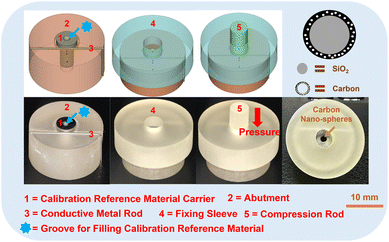
2.4 Design and 3D printing of calibration carrier device
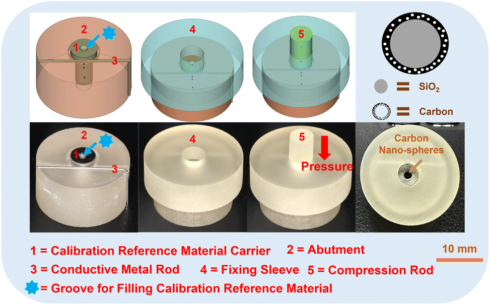
A 3D model of the calibration carrier device was indigenously designed using the Materializes Magics 24.0 software (Materialise, Belgium). As shown in Fig. 2, the device consisted of five parts: the abutment for placing calibration reference material (part 1 and part 2), the conductive metal rod (part 3), the sleeve (part 4) for fixing conductive metal rod and the compression rod (part 5) for compressing the reference material. After the design was completed, the device was 3D printed using Projet MJP 3600 printer (3D Systems, USA) with VisiJet Stoneplast printable resin (3D Systems, USA). The final product is shown in Fig. 2H, where the black region in the center consists of the compressed conductive carbon nanospheres.
 |
| | Fig. 2 Design and 3D printing of calibration carrier device. | |
2.5 Stability and image linear distortion testing
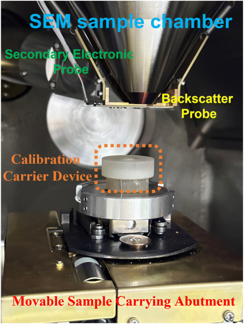
The stability test refers to the particle size statistics of the obtained SEM images under repeated bombardments with different accelerating voltages and image magnifications. The procedure was performed as follows: an initial SEM image was recorded according to the normal operation procedure, a follow-up image was recorded under various acceleration voltages (15 kV, 20 kV and 25 kV) and magnifications (8000×, 10![[thin space (1/6-em)]](https://www.rsc.org/images/entities/char_2009.gif) 000×, 15000× and 20000×). Finally, the aforementioned procedure was repeated until 12 sets of combinations were recorded, where each combination was repeated 4 times to obtain a total of 48 SEM images. It is well known that the damage to the calibration specimen is more pronounced as the accelerating voltage is increased. For the image linearity distortion tests, the same sample area was placed in the center and four corners of the monitor, and a high acceleration voltage of 25 kV and magnification of 15000× were used to record the SEM images. Additionally, 4 images were taken at each position, and a total of 20 SEM images were obtained. The test temperature and ambient humidity were 25 °C and 40%, respectively. The sample chamber of the JSM-IT500 SEM is given in Fig. 3, where the dashed orange line shows the designed and 3D printed calibration carrier device.
000×, 15000× and 20000×). Finally, the aforementioned procedure was repeated until 12 sets of combinations were recorded, where each combination was repeated 4 times to obtain a total of 48 SEM images. It is well known that the damage to the calibration specimen is more pronounced as the accelerating voltage is increased. For the image linearity distortion tests, the same sample area was placed in the center and four corners of the monitor, and a high acceleration voltage of 25 kV and magnification of 15000× were used to record the SEM images. Additionally, 4 images were taken at each position, and a total of 20 SEM images were obtained. The test temperature and ambient humidity were 25 °C and 40%, respectively. The sample chamber of the JSM-IT500 SEM is given in Fig. 3, where the dashed orange line shows the designed and 3D printed calibration carrier device.
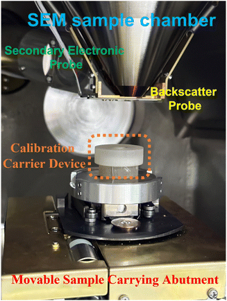 |
| | Fig. 3 JSM-IT500 SEM sample chamber. | |
2.6 Data analyses
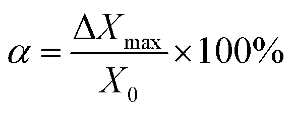
The diameter of carbon nanospheres was measured using the Nanomeasurer 1.2 software in the following steps: firstly, the obtained SEM image was imported into the software, and the true length of the scale and the unit were set according to the SEM image, secondly, the mouse was dragged to select the particles in the SEM image for labeling, and for each labeled particle, the program would record its serial number and particle size. The IBM SPSS Statistics 26.0 software was used to examine the data. The Shapiro–Wilk test was used to test the normality, whereas the homogeneity of variances were measured by the Levene's test.31–33 Considering the small sample size, a residual plot was used to measure the feasibility of the model. Then, a two-way analysis of variance (ANOVA) was employed to analyze possible differences between the microsphere diameters under various accelerating voltages (15 kV, 20 kV and 25 kV) and magnifications (8000×, 10000×, 15000× and 20000×), which were selected as the independent variables. Subsequently, a one-way ANOVA was used to analyze the microsphere diameters measured at the center and corners to ascertain if there was any distortion in the image linearity. Additionally, the diameters of the nanospheres in the X and Y axes at these five positions were measured and noted as X0 − X4 and Y0 − Y4. Taking ΔXi = Xi − X0, ΔYi = Yi − Y0 (i = 1, 2, 3, 4), and ΔXmax and ΔYmax denote the maximum values of |ΔXi| and |ΔYi|, respectively. The linear distortion was calculated using the following equations:
where α and β represent the linear distortion in the X and Y axes, respectively. According to NIST, both α and β should be less than 1%.
3 Results and discussion
3.1 Structural characterization
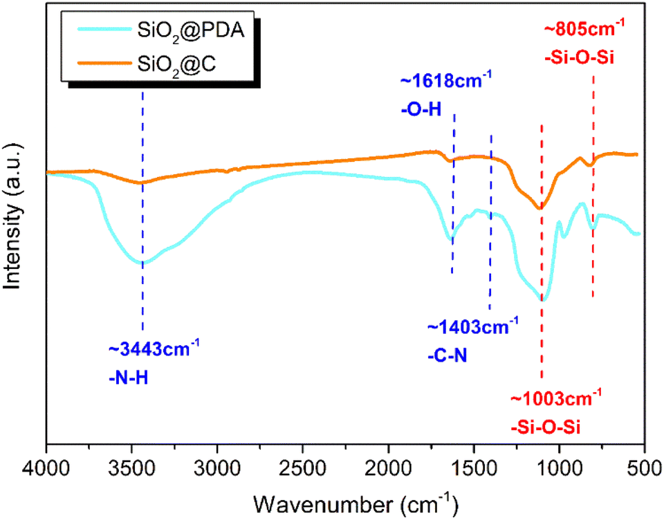
FTIR analysis was performed in order to investigate the chemical structure of the surface functional groups of the precursor SiO2@PDA and the conductive carbon nanospheres, as shown in Fig. 4. In the case of SiO2@PDA, the sharp and broad absorption peak at ∼3443 cm−1 was attributed to the –N–H bond of PDA, the absorption peak at ∼1618 cm−1 was due to the –O–H bond on the PDA, and the absorption peak at ∼1403 cm−1 was attributed to the –C–N bond of the PDA.34,35 Additionally, the absorption peaks at ∼1003 cm−1 and ∼805 cm−1 were attributed to the antisymmetric stretching vibration and symmetric stretching vibration of Si–O–Si bond in SiO2, respectively.36,37 In contrast, the intensity of the absorption peaks at ∼3443 cm−1, 1618 cm−1 and 1403 cm−1 of the conductive carbon nanospheres was significantly reduced, indicating that the PDA underwent different degrees of thermal cracking at 800 °C. However, the characteristic absorption peaks of the inner core SiO2 did not change significantly. These results indicate that the high-temperature heat treatment did not disrupt the main structure of the composite, but only cracked the PDA layer into a conductive carbon layer.
 |
| | Fig. 4 FTIR of the precursor SiO2@PDA and the conductive carbon nanospheres. | |
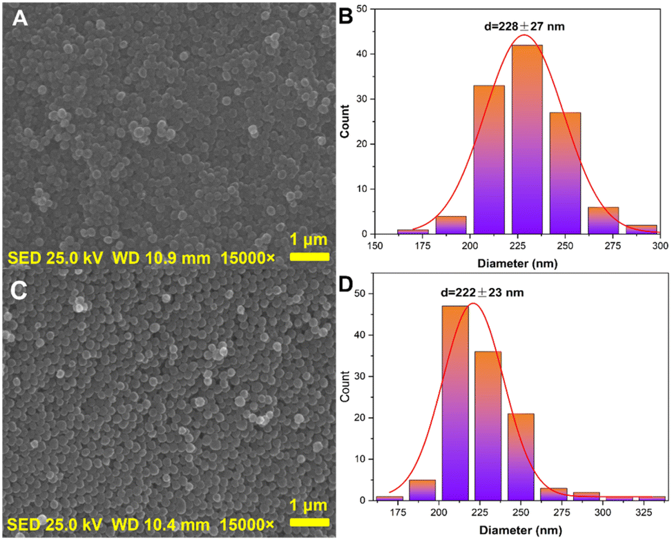
The microscopic morphology of the conductive carbon nanospheres was obtained using SEM in order to further demonstrate that the main structure was retained, as shown in Fig. 5. SEM images of the nanospheres obtained using a single injection and a drop-by-drop addition of TEOS are shown in Fig. 5A and C, respectively, whereas the corresponding particle size statistics of 120 nanospheres are shown in Fig. 5B and D, respectively. Evidently, the conductive carbon nanospheres prepared by the drop-by-drop TEOS addition method had better dispersion, stronger granularity, and less agglomeration. Moreover, the carbon nanospheres obtained by both methods maintained excellent spherical morphology without any obvious broken structures. The average particle size was relatively uniform with 228 ± 27 nm and 222 ± 23 nm for the single injection method and the drop-by-drop TEOS addition method, respectively.
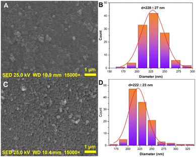 |
| | Fig. 5 SEM images of the nanospheres obtained using a single injection (A and B) and a drop-by-drop addition (C and D) of TEOS. | |
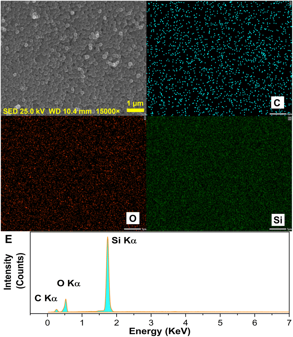
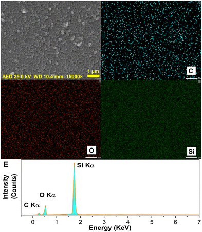
In order to determine the elemental distribution and the content information, SEM-EDS analysis of unsprayed gold carbon nanospheres was directly performed, as shown in Fig. 6. It can be seen that the carbon nanospheres were composed of C, O and Si elements, and the three elements were evenly distributed. The origin of the O and Si elements was attributed to the core SiO2, while C element originated from the carbon layer after the high temperature cracking of PDA. Additionally, the absence of elemental N in the EDS spectrum illustrated that the thermal cracking of PDA was essentially complete. The excellent electrical conductivity was ascribed to the high purity of the carbon layer.
 |
| | Fig. 6 SEM-EDS images and elemental distribution of conductive carbon nanospheres. | |
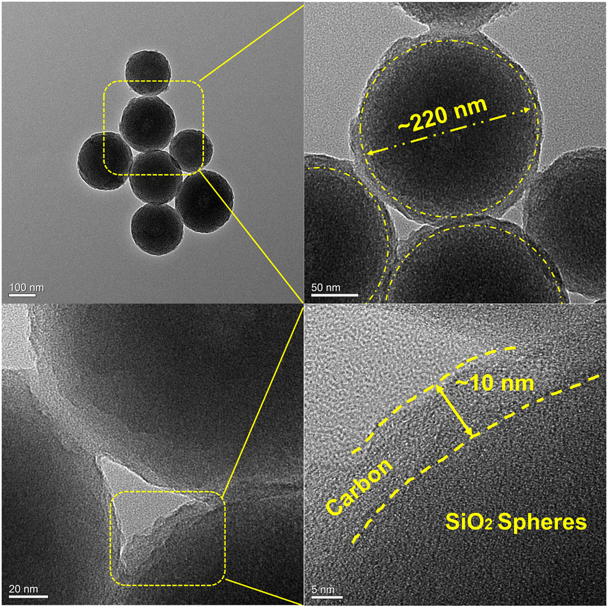
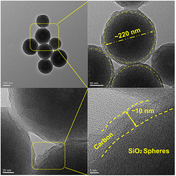
These results demonstrate that the decomposition of PDA into conductive carbon layers by thermal cracking was effective, and the prepared conductive carbon nanospheres had good sphericity and high purity. TEM images were recorded to further examine the nanospheres in terms of the diameter of the core SiO2, the carbon layer encapsulation and the thickness of the nanospheres, as shown in Fig. 7. The carbon nanospheres were found to consist of two parts, which included a spherical SiO2 core (within the circular yellow dashed line) and an outer curly surface carbon layer (yellow dashed straight line). Moreover, the SiO2 core was found to be completely coated by the dense carbon layer without any noticeable defects. Additionally, the diameter of the core SiO2 and the thickness of the carbon layer were measured to be about 220 nm and 10 nm, respectively.
 |
| | Fig. 7 TEM images of conductive carbon nanospheres. | |
3.2 Stability study of conductive carbon nanospheres CRM
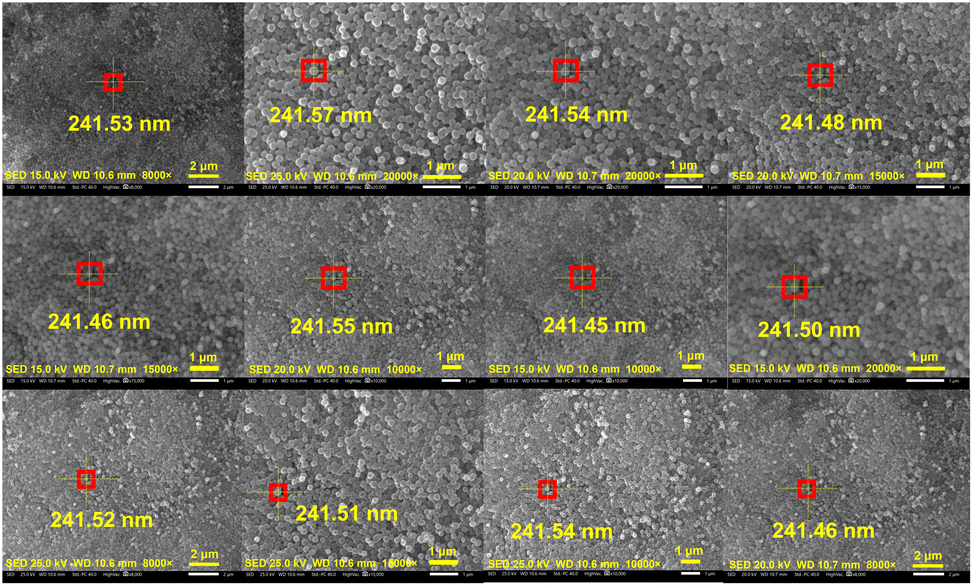
To explore the feasibility of conductive carbon nanospheres as a CRM, the diameter of one fixed microsphere was measured with accelerating voltage and magnification as independent variables, and the microsphere diameter as dependent variable. Moreover, to exclude the influence of environmental factors, the order of experiments was randomized, and each experiment was carried out in the form of 4 parallel experiments. Fig. 8 shows only one of the captured images, and the rest are displayed in Fig. S1–S12.† The data are presented as mean ± SD, as listed in Table 1. After validating the data with Shapiro–Wilk test (Table S1†), Levene's test (Table S2†) and residual plot (Fig. S13†), a two-way ANOVA was used to analyze the data.
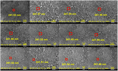 |
| | Fig. 8 SEM images of conductive carbon nanospheres at different accelerating voltages and magnifications. | |
Table 1 Nanosphere diameters measured at different accelerating voltages and magnifications (mean ± SD) and their order of measurement (n = 4)
| Standard order |
Run order |
Accelerating voltage (kV) |
Magnification |
Measured diameter (nm) |
| 1 |
1 |
15 |
8000 |
241.49 ± 0.05 |
| 12 |
2 |
25 |
20000 |
241.54 ± 0.04 |
| 8 |
3 |
20 |
20000 |
241.54 ± 0.08 |
| 7 |
4 |
20 |
15000 |
241.44 ± 0.03 |
| 3 |
5 |
15 |
15000 |
241.51 ± 0.05 |
| 6 |
6 |
20 |
10000 |
241.53 ± 0.03 |
| 2 |
7 |
15 |
10000 |
241.46 ± 0.05 |
| 4 |
8 |
15 |
20000 |
241.53 ± 0.08 |
| 9 |
9 |
25 |
8000 |
241.57 ± 0.04 |
| 11 |
10 |
25 |
15000 |
241.5 ± 0.05 |
| 10 |
11 |
25 |
10000 |
241.52 ± 0.02 |
| 5 |
12 |
20 |
8000 |
241.48 ± 0.06 |
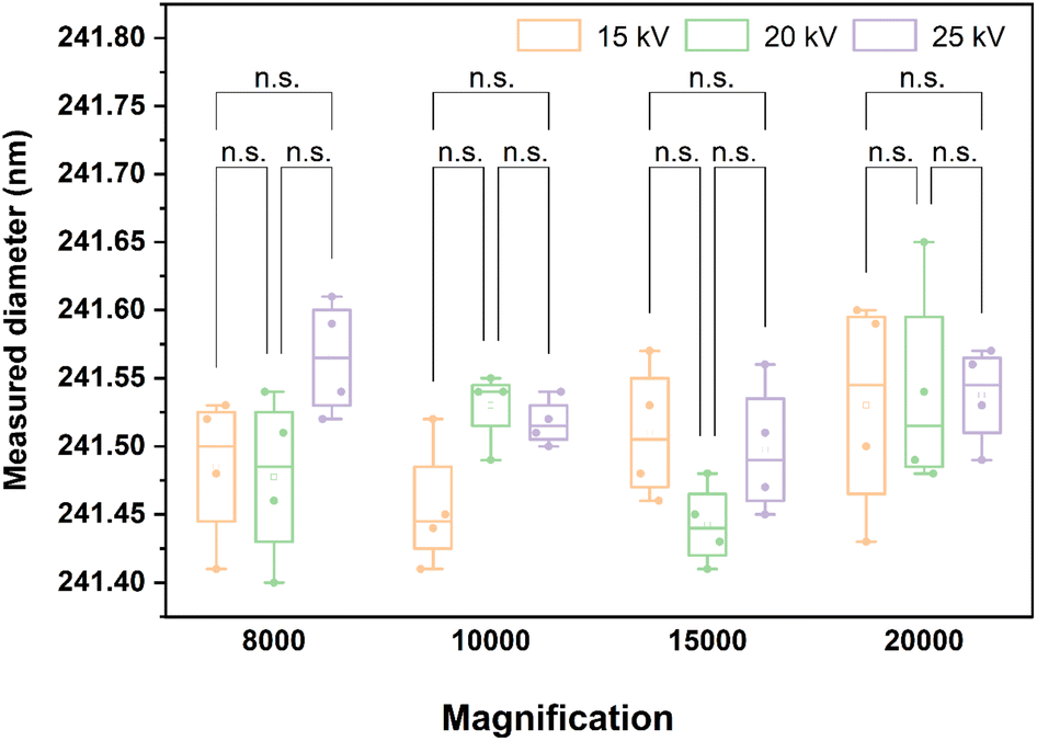
As shown in Table S3,† the two-way ANOVA was used to investigate the influence of accelerating voltage, magnification, and the interaction effect of accelerating voltage and magnification on the detected magnitude of microsphere diameters. As shown in Table S3† and Fig. 9, irrespective of whether it is accelerating voltage, magnification or the interaction effect of the two, the p values are all above 0.05, indicating that they have no significant effect on the detected value of the microsphere diameters.38–40 In other words, under the condition of changing the accelerating voltage and magnification, there is no significant difference between the measured diameter data of microspheres. This result suggests that the nanospheres indeed have the potential to be used as a CRM.
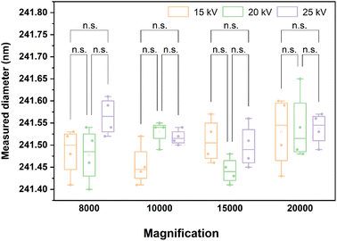 |
| | Fig. 9 Two-way ANOVA plot for nanosphere diameters (independent variables: accelerating voltage and magnification). n.s. means p-value > 0.05 (each scatter in the bar represents a sample). | |
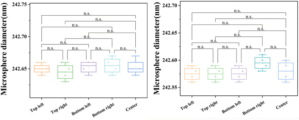
3.3 Linear distortion degree study of conductive carbon nanospheres CRM
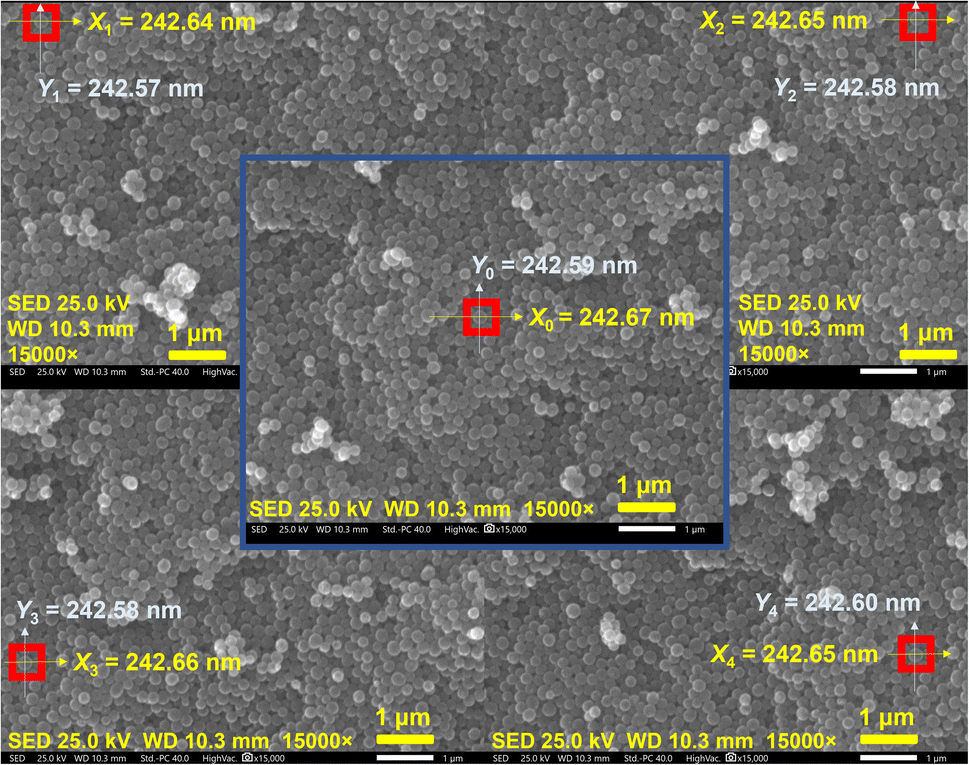
Since accelerating voltage and magnification have no significant effect on the measured diameter of nanospheres, the linear distortion degree of SEM images captured at high accelerating voltage and magnification was investigated. Various positions such as the center and four corners were selected to record SEM images with an accelerating voltage of 25 kV and magnification of 15000. Four parallel inspections were performed at each position. Fig. 10 shows only one of the captured images, and the rest are displayed in Fig. S14–S18.† The data obtained are shown in Table 2. The combined data of Tables S4, S5 and Fig. S19† were considered to pass the normality test and the homogeneity of variance test. Then, in order to explore linear distortion in the captured SEM images, a one-way ANOVA was used to investigate the effect of different imaging positions on the nanosphere diameters. As shown in Table 2, different imaging positions (center and four corners) in the X-axis and Y-axis directions had no significant effect on the nanosphere diameters, which is evident from the p value being greater than 0.05. Furthermore, it can also be clearly seen in Fig. 11 that there were no obvious differences between the nanosphere diameters imaged at various positions. Therefore, from the results shown in Table S6† and Fig. 11, it can be concluded that there was no obvious image linear distortion when the nanospheres were used as the CRM. Taking Fig. 10 as an example, the linear distortion in the X-axis and Y-axis were calculated as α = 0.012% and β = 0.082%, respectively.
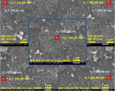 |
| | Fig. 10 SEM images of conductive carbon nanospheres at accelerating voltage of 25 kV and magnification of 15000 (the center and four corners). | |
Table 2 Measured diameters in the X-axis direction and the Y-axis direction, which measured at different position (mean ± SD, n = 4)
| Position |
Measured diameter measured in X direction (nm) |
Measured diameter measured in Y direction (nm) |
| Center |
242.65 ± 0.01 |
242.58 ± 0.01 |
| Top left |
242.65 ± 0.01 |
242.58 ± 0.01 |
| Top right |
242.65 ± 0.01 |
242.58 ± 0.01 |
| Bottom left |
242.66 ± 0.01 |
242.6 ± 0.01 |
| Bottom right |
242.66 ± 0.02 |
242.58 ± 0.02 |
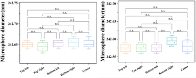 |
| | Fig. 11 One-way ANOVA plot of photographing positions for measured diameters in the X-axis direction and the Y-axis direction. n.s. means p-value > 0.05 (each scatter in the bar represents a sample). | |
Finally, Table 3 shows the comparison between the CRMs commonly used at NIST and the carbon nanospheres in this paper, and it can be seen that as a non-metallic material, carbon nanospheres have nanoscale size with a diameter of 200–240 nm and excellent physical/chemical stability. As mentioned previously, carbon nanospheres had been proven to be a CRM with stable calibration effect. Hence in practical operation, it is placed in the SEM sample chamber that needs to be calibrated and several SEM photographs are taken at different accelerating voltages and magnifications. And choosing any nanosphere for diameter measurement, the smaller the diameter variability, the better the accuracy of the SEM equipment. Compared to traditional CRMs, carbon nanospheres can be synthesized in bulk at the laboratory level while enabling rapid calibration.
Table 3 Comparison of different types of CRMs
| CRMs |
Material |
Diameter |
Manufacturing process41,42 |
Chemical stability in humid air |
Coefficient of thermal expansion (CTE), α (10−6 K−1, 20 °C)43–46 |
| Lithographically patterned silicon chips (NIST, USA) |
Semiconductor |
50–1500 μm |
Lithographic printing |
Stable |
2.4 |
| Gold nanoparticles on a silicon chip (NIST, USA) |
Precious metal |
10–60 nm |
Arc plasma deposition system |
Stable |
14.2 |
| Copper grids (NIST, USA) |
Metal |
1–50 μm |
Arc plasma deposition system |
Unstable |
16.5–18.4 |
| 2Cu + O2 + CO2 + H2O = Cu2(OH)2CO3 |
| Carbon nanospheres (this work) |
Non-metal |
200–240 nm |
Chemical coating |
Stable |
Carbon (0.5–2.0) |
| Silicon dioxide (2.2–2.6) |
4 Conclusion
In this paper, a novel reference material for SEM calibration was synthesized in the form of conductive carbon nanospheres. Oxidative self-polymerization of dopamine (DA) was used to form a polydopamine (PDA) layer on the surface of the synthesized silicon dioxide, and the PDA layer was decomposed into a carbon layer with excellent electrical conductivity via thermal treatment. The preparation process was comparatively simple and facilitated bulk synthesis at the laboratory level.
FTIR analysis results indicated that the main structure of the composite was retained upon high-temperature heat treatment. The PDA layer underwent cracking and transformed into a conductive carbon layer. SEM and EDS analysis results showed that the prepared conductive carbon nanospheres were of excellent sphericity and high purity with an average particle size of ∼222 ± 23 nm. TEM analysis results showed that the diameter of the core silicon dioxide and the thickness of the carbon layer were ∼220 nm and ∼10 nm, respectively. Importantly, the two-way ANOVA revealed that the accelerating voltage and magnification had no significant effect on the diameter of the microspheres. Simultaneously, the one-way ANOVA showed that there were no significant differences in the measured diameters at various positions measured in the X-axis and Y-axis directions (p > 0.05).
Overall, the prepared conductive non-metallic carbon nanospheres CRM was found to be well stabilized under high vacuum and repeated bombardment with different accelerating voltages. This was validated by the fact that the captured 68 SEM images exhibited excellent resolution with no obvious distortion and shift. Moreover, the designed and 3D printed calibration carrier device also facilitated the calibration process. The carbon nanospheres CRM designed and synthesized in this paper are expected to further replace conventional metallic CRMs for routine SEM calibration.
Author contributions
ManLu Wang: methodology, investigation, data curation, writing – original draft, writing – review & editing. JiaCheng Wu: methodology, validation, investigation. LiYing Hao: conceptualization, resources, data curation. Qiang Wei: data curation, methodology, resources, writing – review & editing, supervision, writing – original draft, funding acquisition.
Conflicts of interest
There are no conflicts to declare.
Acknowledgements
This work is financially supported by Experimental Technology Research Project of Sichuan University (SCU221078).
References
- R. Chen, J. Lv and J. Feng, Anal. Lett., 2015, 48, 1502–1510 CrossRef CAS.
- J. Liu, J. Microsc., 2021, 282, 258–266 CrossRef CAS.
- M. Luckner and G. Wanner, Microsc. Microanal., 2018, 24, 526–544 CrossRef CAS PubMed.
- M. O. Pereira, Spectrochim. Acta, Part A, 2021, 246, 118925 CrossRef CAS PubMed.
- V. A. J. Jaques, E. Zikmundová, J. Holas, T. Zikmund, J. Kaiser and K. Holcová, Sci. Rep., 2022, 12, 19650 CrossRef CAS PubMed.
- X. D. Zhang, L. Zhao, S. Y. Li, Z. G. Han, X. Q. Xu and A. H. Wu, Acta Metall. Sin., 2022, 43, 1544–1548 Search PubMed.
- L. Z. Yu, Exp. Sci. Tech., 2022, 20, 81–85 Search PubMed.
- Z. Hu, M. M. Han, C. Chen, Z. D. Zou, Y. Shen, Z. Fu, X. G. Zhu, Y. X. Zhang, H. M. Zhang, H. J. Zhao and G. Z. Wang, Appl. Catal., B, 2022, 306, 121140 CrossRef CAS.
- F. Wang, Y. M. Zhang, Q. L. Fang, Z. Y. Li, Y. X. Lai and H. S. Yang, Chemosphere, 2021, 263, 128109 CrossRef CAS PubMed.
- J. Q. Yu, D. P. Cai, J. H. Si, H. B. Zhan and Q. T. Wang, J. Mater. Chem. A, 2022, 10, 4100–4109 RSC.
- Y. T. Liu, J. Chem. Technol. Biotechnol., 2022, 97, 1758–1762 CrossRef CAS.
- X. Y. Xu, X. Chen, H. Y. Wu, B. Xie, D. G. Wang, R. Wang, X. Y. Zhang, Y. Z. Piao, G. W. Diao and M. Chen, Carbon, 2022, 187, 354–364 CrossRef.
- F. C. Meng, S. W. Wang, B. H. Jiang, L. Ju, H. J. Xie, W. Jiang and Q. M. Ji, Nanoscale, 2022, 14, 10389–10398 RSC.
- M. Y. Emran, M. A. Shenashen, A. Elmarakbi, M. M. Selim and S. A. EI-Safty, Anal. Chim. Acta, 2022, 1192, 339380 CrossRef CAS PubMed.
- N. E. Grant, S. L. Pain, J. T. White, M. Walker and I. Prokes, ACS Appl. Energy Mater., 2022, 5, 1542–1550 CrossRef CAS.
- M. Naorem, R. Singh and R. Paily, IEEE Sens. J., 2021, 21, 22426–22433 CAS.
- M. Fatma, E. Demerdash, A. Mohammed and A. Raghda, Environ. Toxicol., 2021, 36, 1362–1374 CrossRef PubMed.
- W. X. Zhao, X. Q. Ma, L. C. Yue, L. C. Zhang, Y. S. Luo, Y. C. Ren, X. E. Zhao, N. Li, B. Tang, Q. Liu, Y. Liu, S. Y. Gao, A. A. Ali and X. P. Sun, J. Mater. Chem. A, 2022, 10, 4087–4099 RSC.
- C. Thieme, J. Am. Ceram. Soc., 2022, 105, 3544–3554 CrossRef CAS.
- M. D. Purkayastha, M. T. Pal, M. Sarkar and S. Ghosh, Radiat. Phys. Chem., 2022, 192, 109898 CrossRef CAS.
- Z. H. Zhao, H. L. Zhu and J. R. Huang, ACS Catal., 2022, 12, 7986–7993 CrossRef CAS.
- P. Wang, Y. L. Zhang, K. L. Fu, Z. Liu, L. Zhang, C. Liu, Y. Deng, R. Xie, X. J. Ju, W. Wang and L. Y. Chu, Mater. Adv., 2022, 3, 5476–5487 RSC.
- X. F. Fan, H. C. Mu, Y. L. Xu, C. W. Song and Y. M. Liu, Int. J. Energy Res., 2022, 46, 8949–8961 CrossRef CAS.
- M. Sabeti, A. A. Ensafi, K. Z. Mousaabadi and B. Rezaei, IEEE Sens. J., 2021, 21, 19714–19721 CAS.
- Y. X. Chen, Y. Jiang, W. Q. Feng, W. Wang and D. Yu, Colloids Surf., A, 2022, 635, 128055 CrossRef CAS.
- Y. Xiong, L. Jiang, G. X. Yao, L. X. Duan and S. Z. Wang, Biochem. Eng. J., 2022, 180, 108370 CrossRef CAS.
- Y. L. Miao, X. W. Zhou, J. Bai, W. S. Zhao and X. B. Zhao, Chem. Eng. J., 2022, 430, 133089 CrossRef CAS.
- L. L. Cao, Z. X. Kou, W. B. Chao, S. J. Yuan, Z. C. Huang, B. You, J. Du and Y. Zhai, J. Magn. Magn. Mater., 2022, 546, 168909 CrossRef CAS.
- X. F. Qin, H. Wu, C. Y. Chen, H. Ao, W. C. Li, R. L. Gao, W. Cai, G. Chen, X. L. Deng, Z. H. Wang, X. Lei and C. L. Fu, J. Alloys Compd., 2022, 890, 161869 CrossRef CAS.
- M. M. Algaradah, J. Anal. Chem., 2021, 12, 446–457 CAS.
- H. Yu and T. Huan, Anal. Chim. Acta, 2022, 1200, 339614 CrossRef CAS PubMed.
- G. Dinç, A. K. Salihoğlu, B. Ozgoren, S. Akkaya and A. Ayar, J. Magn. Reson. Imaging, 2022, 55, 1761–1770 CrossRef PubMed.
- W. Chen, Q. Wei, W. Huang, J. Chen, S. Hu, X. Lv, L. Mao, B. Liu, W. Zhou and X. Liu, Eur. J. Radiol., 2022, 148, 110155 CrossRef.
- G. H. Liu, Q. S. Xiong, Y. Q. Xu, Q. L. Fang, K. C. Leung, M. Sang, S. H. Xuan and L. Y. Hao, Colloids Surf., A, 2022, 633, 127860 CrossRef CAS.
- L. Gu, J. Guan, Z. W. Huang, H. Y. Huo, S. Shi, D. X. Zhang and F. Yan, Electrophoresis, 2022, 43, 1446–1454 CrossRef CAS PubMed.
- L. Xu, H. Lei, Z. Y. Ding, Y. Chen, R. Y. Ding and T. S. Kim, Powder Technol., 2022, 395, 338–347 CrossRef CAS.
- M. F. Zawrah and B. G. Alhogbi, Ceram. Int., 2021, 47, 23240–23248 CrossRef CAS.
- L. Yu, J. D. Zhang, Y. Liu, L. Y. Chen, S. Tao and W. X. Liu, Sci. Total Environ., 2021, 756, 143860 CrossRef CAS PubMed.
- P. Yin, S. W. Xie, Z. X. Zhuang, X. S. He, X. P. Tang, L. X. Tian, Y. J. Liu and J. Niu, Aquaculture, 2021, 531, 735864 CrossRef CAS.
- R. W. Brown, D. R. Chadwick, H. Thornton, M. R. Marshall, S. Bei, M. Distaso, R. Bargiela, K. A. Marsden, P. L. Clode, D. V. Murphy, S. Pagella and D. L. Jones, Soil Biol. Biochem., 2022, 165, 108496 CrossRef CAS.
- M. S. Radue, Y. Mo and R. E. Butera, Chem. Phys. Lett., 2022, 787, 139258 CrossRef CAS.
- J. H. Quintero, P. J. Arango, R. Ospina, A. Mello and A. Marino, Surf. Interface Anal., 2016, 47, 701–705 CrossRef.
- V. Vodickova, P. P. Prokopcakova, M. Svec, P. Hanus, J. Moravec and L. Camek, J. Manuf. Sci. Eng. Trans. ASME, 2022, 22, 95–101 Search PubMed.
- N. T. Hoa, N. Q. Hoc and H. X. Dat, Physics, 2023, 5, 59–68 CrossRef.
- S. H. Lee, H. S. Sung, J. S. Kim, J. Yesuraj, K. Kim and H. R. Seo, Int. J. Energy Res., 2022, 46, 10917–10918 Search PubMed.
- L. Zhou, K. Y. Liu, T. B. Yuan, Z. Y. Liu, Q. Z. Wang, B. L. Xiao and Z. Y. Ma, J. Mater. Res. Technol., 2022, 18, 3478–3491 CrossRef CAS.
|
| This journal is © The Royal Society of Chemistry 2023 |
Click here to see how this site uses Cookies. View our privacy policy here. 
 Open Access Article
 This Open Access Article is licensed under a Creative Commons Attribution-Non Commercial 3.0 Unported Licence
 *a
*a