
 Open Access Article
 This Open Access Article is licensed under a Creative Commons Attribution-Non Commercial 3.0 Unported Licence
Theoretical investigations of the electronic and optical properties of a GaGeTe monolayer
Nguyen Thi Han *a,
Vo Khuong Diena,
Tay-Rong Chang*abc and
Ming-Fa Linad
*a,
Vo Khuong Diena,
Tay-Rong Chang*abc and
Ming-Fa Linad
aDepartment of Physics, National Cheng Kung University, 1 University Road, Tainan, 70101, Taiwan. E-mail: han.nguyen.dhsptn@gmail.com; u32trc00@phys.ncku.edu.tw
bCenter for Quantum Frontiers of Research and Technology (QFort), Tainan, 70101, Taiwan
cPhysics Division, National Center for Theoretical Sciences, Taipei, 10617, Taiwan
dHierarchical Green-Energy Material (Hi-GEM) Research Center, National Cheng Kung University, Taiwan
First published on 27th June 2023
Abstract
Our study focused on exploring the electronic and optical characteristics of the GaGeTe monolayer using first-principles calculations. Our findings showed that this material has remarkable physical and chemical properties attributed to its unique band structure, van Hove singularities in the density of states (DOS), charge density distributions, and charge density differences. We also observed excitonic effects, multiple optical excitation peaks, and strong plasmon modes in the energy loss functions, absorption coefficients, and reflectance spectra, which contribute to its enriched optical response. Moreover, we were able to establish a close relationship between the orbital hybridizations of the initial and final states with each optical excitation peak. Our results suggest that GaGeTe monolayers hold great potential for various semiconductor applications, especially those involving optics. Furthermore, the theoretical framework we used can be applied to study the electronic and optical properties of other graphene-like semiconductor materials.
1. Introduction
In 2004, Geim and colleagues achieved the first known extraction and discovery of single-layer graphene through the backward exfoliation of graphite.1 Graphene is a fantastic material for transparent and conductive composites, electrodes, and nanotechnology applications.2,3 However, graphene lacks a band gap, which is required for some electronic devices, such as transistors.4 As a consequence, significant effort has been expended to investigate functional two-dimensional (2D) semiconductors with high carrier mobility, large tunable band gap, and high stability.5,6 In recent years, 2D materials7–9 are known to exhibit rich electronic, magnetic, and optical properties, such as superconductivity, ferromagnetism, semi-conductivity, and so on. For instance, a large number of 2D materials, such as MoX2, WX2, GaX, and InX (X = S, Se, Te) have been researched in both theoretical simulations and experimental measurements.10–13Searching for 2D stable germanene-based films14,15 with intrinsic semiconducting character, instead of obtaining this characteristic by tuning via different means, is desired and perhaps is a suitable way to realize its practical applications. Among them, the GaGeTe monolayer is derived from a 3D bulk one that has been synthesized successfully by using the Bridgman technique.16 Several experimental techniques can be used to investigate the properties of monolayer GaGeTe. For instance, high-resolution tunneling electron microscopy (HRTEM)16,17 has been used to obtain a side view of the material, while angle-resolved photoemission spectroscopy (ARPES)18,19 has been utilized to reveal its occupied states in calculated electronic properties. High-resolution scanning tunneling spectroscopy (STS)20,21 can examine the entire occupied and unoccupied states of van Hove singularities in the density of states (DOS). Unfortunately, these techniques have not been applied to study monolayer GaGeTe, and further experimental research is needed to investigate its electronic properties. In addition, the optical and transport properties of the GaGeTe single crystals have been previously reported using a modified Bridgman technique in 2013, showing an optical band gap Eg = 1.12 eV.22
Despite obtaining some outcomes through first-principles simulations, the results concerning the GaGeTe monolayer are still limited. For instance, Jin Zhang and his partner23 have reported that the GaGeTe monolayer possessed an indirect gap semiconductor of 0.65 eV by using density functional theory (DFT level). In addition, Congming Ke24 has studied the electronic properties of GaGeTe monolayer, indicating indirect gap semiconductor nature of 0.54 eV and 1.15 eV by using the DFT level and Heyd–Scuseria–Ernzerhof (HSE) standard. Also, Lili Xu et al.25 have reported the electronic properties of the GaGeTe monolayer by using the DFT level, showing an indirect gap semiconductor of 0.72 eV. In short, the considerations of the GaGeTe monolayer on electronic properties and optical responses with/without excitonic effect are still limited. Understanding the chemical bonding in the GaGeTe monolayer is crucial for further exploring its physical and chemical properties. As of yet, there have been no examinations conducted to elucidate the specific chemical and physical traits associated with orbital hybridization in chemical bonds. Therefore, further theoretical research is needed to explore the nature of the chemical bonding in the GaGeTe monolayer and provide a more comprehensive understanding of its physical and chemical properties.
Our utilized first-principles calculations to explore the ideal geometric structure, electrical and wave functions, and optical properties of monolayer GaGeTe. Our results revealed rich and distinctive characteristics, such as an optimized geometric structure with position-dependent chemical bonding, band structure, and the atom-dominated energy spectrum at various energy ranges. We also calculated the charge density distribution and charge density difference due to different orbitals, and the atom-and orbital-projected density of states connected to the mixed orbitals. Additionally, we explored the dielectric function, absorption spectrum, reflectivity, and energy loss function of the optical characteristics, which provided insights into the material's optical response. We also established a close relationship between electronic properties, optical excitations, and orbital hybridizations. Our findings can facilitate a better understanding of various phenomena and multiple applications of monolayer GaGeTe, using the developed theoretical framework which was successfully published in previous studies.26–30
2. Calculation methods
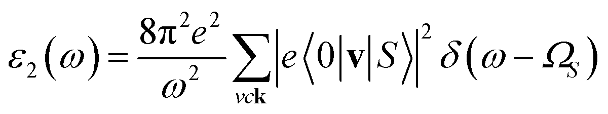
The density functional theory31 via Vienna Ab initio Simulation Package (VASP)32 is utilized to investigate the optimal geometric structure and electronic and optical properties of the GaGeTe monolayer. The Perdew–Burke–Ernzerhof generalized gradient approximation was used for the exchange–correlation functions.33–36 The projector-augmented wave method37 was utilized for the characterization of the ion and valence electron interactions. The cutoff energy for the expansion of the plane wave basis was set to 450 eV. The Brillouin zone was integrated with a special k-point mesh of 35 × 35 × 1 in the Γ-centered sampling technique for the structural optimization.38 The convergence condition of the ground state is set to be 10−8 eV between two consecutive simulation steps, and all atoms could fully relax during the geometric optimization until the Hellmann–Feynman force acting on each atom was smaller than 0.01 eV. The HSE06 method39 is added to get more band gaps. To evaluate the dynamic stability of the GaGeTe monolayer, the phonon energy dispersions were calculated within the harmonic approximations by using density functional perturbation theory as implemented in the PHONOPY code.40 In these calculations, neighboring interactions (corresponding to 5 × 5 × 1 supercell) have been taken into account to get a reliable phonon band structure.On the top of DFT wave functions, the quasi-particle energies are obtained within approximation for the self-energy, the cutoff energy for the response function was set to 120 eV, and 12 × 12 × 1 Γ-centered points sampling was used to represent reciprocal space. The Wannier interpolation procedure performed in the WANNIER90 code41 was used to plot the accurate GW structure. The single particle excitation spectra, which are related to the imaginary part of the dielectric functions ε2(ω), could be described by the following Fermi's golden role:42
 | (1) |
In addition to the single-particle excitations, the presence of stable exciton may strongly affect the optical properties. To evaluate this bound state of the electron–hole pair, we solve the standard Bethe–Salpeter equation (BSE).43
 | (2) |
Noted that the k-point sampling, energy cutoff, and the number of bands, were set to the same values as in the GW level. The close connection of the initial and the final orbital hybridizations with the prominence of optical excitations, and the effects of the electron–hole couplings on the optical properties are the main study focus of the current work. Other optical properties, such as the energy loss functions,44 absorption coefficient,45 and reflectivity46 can be obtained from the dielectric function by following equations:
 | (3) |
 | (4) |
 | (5) |
![[small sigma, Greek, tilde]](https://www.rsc.org/images/entities/i_char_e10d.gif) (ω) = σ2D(ω)/ε0c is the normalized conductivity.
(ω) = σ2D(ω)/ε0c is the normalized conductivity.
3. Results and discussions
3.1 Electronic and optical excitations
Trigonal R![[3 with combining macron]](https://www.rsc.org/images/entities/char_0033_0304.gif) m space group is the crystallization space for GaGeTe bulks (3D)47 (Fig. 1(a)) which include three GaGeTe sheets. The GaGeTe monolayer, a single hextuple-layer in the Te–Ga–Ge–Ge–Ga–Te sequence, exfoliates from 3D one to construct a monolayer (2D) made up of strongly bound germanene sandwiched between two-atom thick GaTe fragments (Fig. 1(b) and (c)). The lattice parameters, a = 4.13 and c = 36.66 are shown via structural optimization to be in good agreement with the previous results.23 Here, Ga3+ forms GaGeTe3 tetrahedra that share corners with three equivalent GeGaGe3 tetrahedra and corners with six equivalent GaGeTe3 tetrahedra. The Ga–Ge and Ge–Ge bonds have a length of 2.47 Å and 2.51 Å, respectively. The average Ga–Te bond lengths are 2.69 Å. As a result, the predictions of pure and impure sp3–sp3 hybridizations in all Ga–Ge, Ge–Ge, and Ga–Te chemical bonds are responsible for featured properties, and strong optical excitations. The side- and top-view nanoscale geometries can be tested by tunneling electron microscopy (TEM) and scanning tunneling microscopy (STM), respectively for GaGeTe monolayer.16
m space group is the crystallization space for GaGeTe bulks (3D)47 (Fig. 1(a)) which include three GaGeTe sheets. The GaGeTe monolayer, a single hextuple-layer in the Te–Ga–Ge–Ge–Ga–Te sequence, exfoliates from 3D one to construct a monolayer (2D) made up of strongly bound germanene sandwiched between two-atom thick GaTe fragments (Fig. 1(b) and (c)). The lattice parameters, a = 4.13 and c = 36.66 are shown via structural optimization to be in good agreement with the previous results.23 Here, Ga3+ forms GaGeTe3 tetrahedra that share corners with three equivalent GeGaGe3 tetrahedra and corners with six equivalent GaGeTe3 tetrahedra. The Ga–Ge and Ge–Ge bonds have a length of 2.47 Å and 2.51 Å, respectively. The average Ga–Te bond lengths are 2.69 Å. As a result, the predictions of pure and impure sp3–sp3 hybridizations in all Ga–Ge, Ge–Ge, and Ga–Te chemical bonds are responsible for featured properties, and strong optical excitations. The side- and top-view nanoscale geometries can be tested by tunneling electron microscopy (TEM) and scanning tunneling microscopy (STM), respectively for GaGeTe monolayer.16
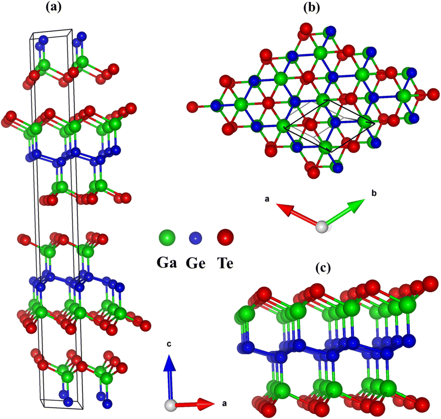 | ||
| Fig. 1 (a) Geometric structure of GaGeTe bulk, (b and c) geometric structure of GaGeTe monolayer, respectively at top view, and side view; noted that the unit cell is black, the Ga, Ge, Te atoms are green, blue, red balls. | ||
Fundamentally, the lattice dynamics or lattice vibration is directly related to the thermodynamic properties of a solid-state material. The phonon dispersion spectrum may offer vital information about the stability of the crystal. In the first Brillouin zone, we calculate the phonon spectra along high symmetric points. Only real modes are present in the phonon dispersion curves of the GaGeTe monolayer, as shown in Fig. 2(a), which indicates strong kinetic stability. There are six atoms in the unit cell, showing three acoustic branches and 15 optic modes. For out-of-plane vibrations, the acoustic phonons have a flexural branch (ZA), while for in-plane vibrations, they have two linear branches (transverse (TA) and longitudinal (LA)). The quadratic energy dispersion of the ZA branch is comparable to that of other two-dimensional materials.48
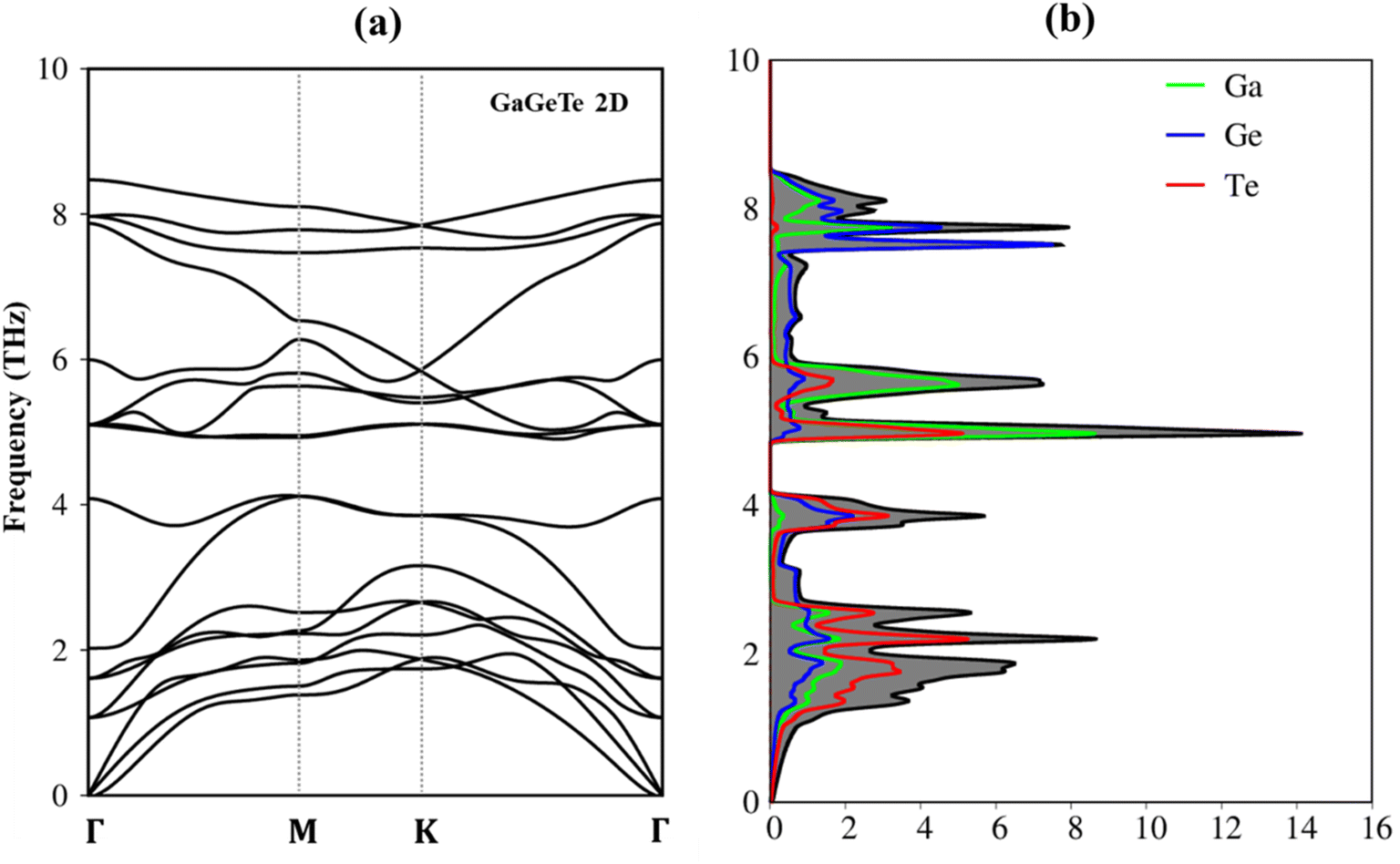 | ||
| Fig. 2 (a) The phonon dispersions of the GaGeTe monolayer, (b) the vibrational density of states of GaGeTe monolayer. | ||
As observed in Fig. 2(b), the corresponding phonon density of states reveals that Te atoms are the principal contributors to the low-frequency phonon modes in the region from 0.00 cm−1 to 160 cm−1 (0.0 THz to 4.0 THz) and the high-frequency photonic modes between 5.2 THz and 8.5 THz (210 cm−1 and 320 cm−1) above the gap. The contributions from the hybridizations between the Te and Ga atoms become dominant in the middle-frequency range between 4.0 THz and 5.2 THz (between 175 cm−1 and 210 cm−1). As a result, the remarkable chemical tunability and orbital interactions of Te atoms will drastically alter phonon characteristics and have the potential to greatly reduce lattice thermal conductivity. In addition to investigating the vibration of atoms at low temperatures, prior studies employing molecular dynamics (MD) calculations23 have also confirmed the stability of this material even under high-temperature conditions. Consequently, the GaGeTe monolayer is suitable for functioning reliably at room temperature.
In addition to the special and stable structures, the GaGeTe monolayer is expected to exhibit remarkable electronic properties. Here, the monolayer GaGeTe displays unique electronic properties along the high-symmetry points in the energy range from −14.0 eV to 4.0 eV as can show in the Fig. 3(a)–(d). Both main features and critical mechanisms are examined in detail from the quasiparticle viewpoints, being closely related to the other essential properties in this study. A thorough comparison with those of graphene-related systems can present certain important differences and thus deduce the significant roles of pure/impure chemical bonds.
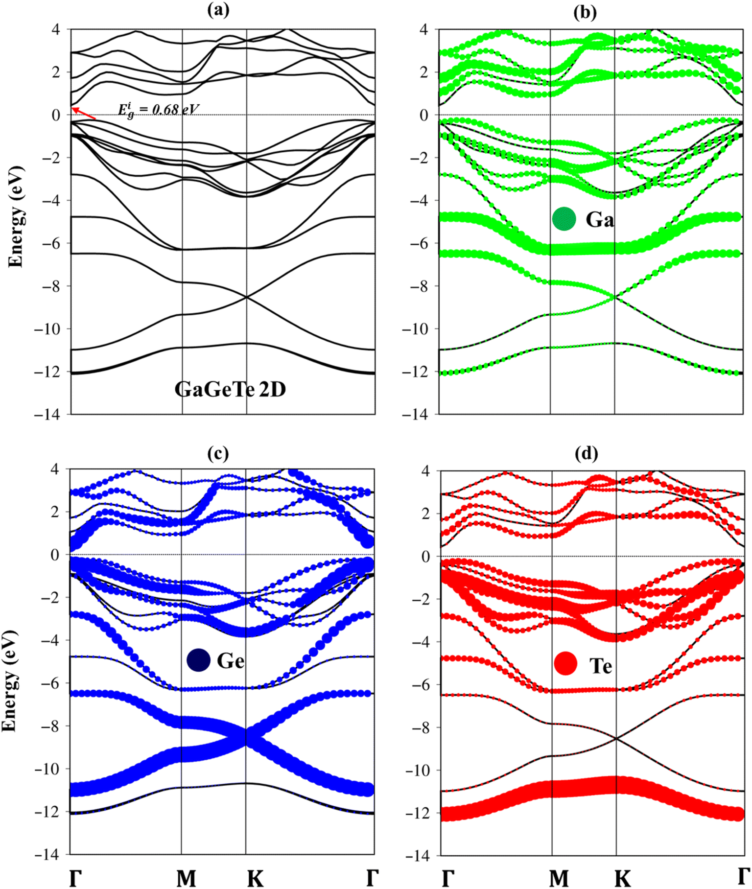 | ||
| Fig. 3 (a) Band structure of GaGeTe monolayer, showing indirect nature, (b–d) the Ga, Ge, Te atoms of contributions in the whole band structure, respectively green, blue, and red circles. | ||
Both the valence band and conduction ones of the GaGeTe monolayer showed many sub-bands with parabolic/oscillatory/sombrero shapes. In particular, the Dirac cone shape appears at a deeper band structure (−10.0 eV to −6.0 eV). The hole states at valence bands and electron ones at conduction bands are highly asymmetrical to each other about the Fermi level EF = 0. In most cases, the band-edge states with vanishing group velocities are provided the unusual structures and can create van Hove singularities in the density of states. Moreover, it is difficult to observe σ, π sub-bands in these systems to compare graphene because of buckling geometric with four sub-lattices. Most importantly, the band structure of the GaGeTe monolayer belongs to the indirect gap semiconductor because of the lowest unoccupied at the Γ point and highest occupied states in between the Γ–M point directions. Our results indicate that the band gap of the GaGeTe monolayer using DFT, and HSE levels is 0.68 eV, and 0.67 eV, respectively. Regarding spin-orbital couplings (SOC), the DFT + SOC calculation reveals that GaGeTe exhibits an indirect band gap of 0.59 eV. The corrections are found to be negligible, leading us to ignore relativistic effects in our calculations to reduce computational costs. Considering that the electronic band gap of semiconductors is often underestimated when using the DFT framework, we have employed the high-precision GW calculation method to obtain an accurate band structure, showing an indirect band gap of 2.10 eV for the GaGeTe monolayer. The observed increase in the electronic band gap can be attributed to the electron–electron self-energy effects, as extensively discussed in numerous prior publications.26,27,30,49–51
The electronic wave functions for the hole and electronic states can offer some insight into the chemical bonding in addition to the main characteristics of the band structure. Each band state can be viewed as a linear superposition of various orbitals. As a result, it can be divided into distinct atomic contributions. The various atom dominances, which are proportional to the spheric radius, can help to explain the critical roles that chemical bonds take part in electronic properties. The contributions from Ga, Ge, and Te are represented by the green, purple, and red balls, respectively. In general, the effective valence and conduction states, which are closely related to the orbital hybridizations of Ga–Te, Ga–Ge, and Ge–Ge bonds (discussed later in Fig. 5), lie in the energy range of −14.0 eV, Ec,v, 4.0 eV. All three atoms have significant contributions to the whole band structure. The Ga, Ge, and Te atoms contributed to the entire band structure by showing green, blue, and red balls (Fig. 3(b)–(d)), linking well van Hove singularities in the density of states in Fig. 5(a)–(d). The Te atoms are located mainly in valence states since their ionization energy is larger than Ga, and Ge atoms. Especially, the Te-5p states contributed mainly to valence bands, and the Ga-4s states contributed mainly to conduction bands (Fig. 6(b)).
To better comprehend the potential applications of the GaGeTe monolayer, we calculated the effective masses (m*) of the conduction band and valence ones along Γ–M directions according to m* = ℏ2(∂2E/∂K2)−1. The obtained results of electron  and hole
  effective masses are equal to 0.057 and 0.318, respectively, suggesting that the carrier mobility of electrons states is faster than that of holes, and thus, is useful for selectively injecting or emitting holes or electrons in nano-electronic devices. Impressively, the mobility of electrons23 reaches up to 7.83 × 104 cm2 V−1 s−1. This remarkably high level of carrier mobility demonstrates the immense potential of the GaGeTe monolayer for various applications, including high-efficiency solar cells and high-speed electronic devices.
To explain the nature and specific orbital hybridizations in chemical bonds of GaGeTe monolayer, Fig. 4(a) and (c) showed its charge density distributions (ρ) and charge density difference (Δρ). The latter could be achieved by the subtraction of the GaGeTe charge density with that of insolated Ga, Ge, and Te atoms. In general, the chemical bonding between Ge–Ge, Ga–Ge, and Ga–Te is characterized by a covalent nature, as the charge density is primarily distributed between the adjacent atoms. Specifically, the germanium sheet is situated between the upper and lower GaTe layers, exhibiting strong hybridization and forming sp3 bonding configurations. In terms of specific orbital hybridizations, it is predicted that the s, px, py, and pz orbitals of Ga, Ge, and Te atoms actively participate in the chemical interaction. This is evidenced by the significant deformation of the spherical distributions surrounding the Ga, Ge, and Te atoms (Fig. 4(b)) compared to their isolated states (Fig. 4(a)). The verification of this phenomenon is further supported by the observation of inhomogeneous redistribution of charge density, as depicted in the charge density difference (Fig. 4(c)). In short, the GaGeTe monolayer provides highly non-uniform chemical environments and is responsive to their diverse properties. These behaviors can connect well with complex band structures and van Hove singularities in the density of states (discuss later).
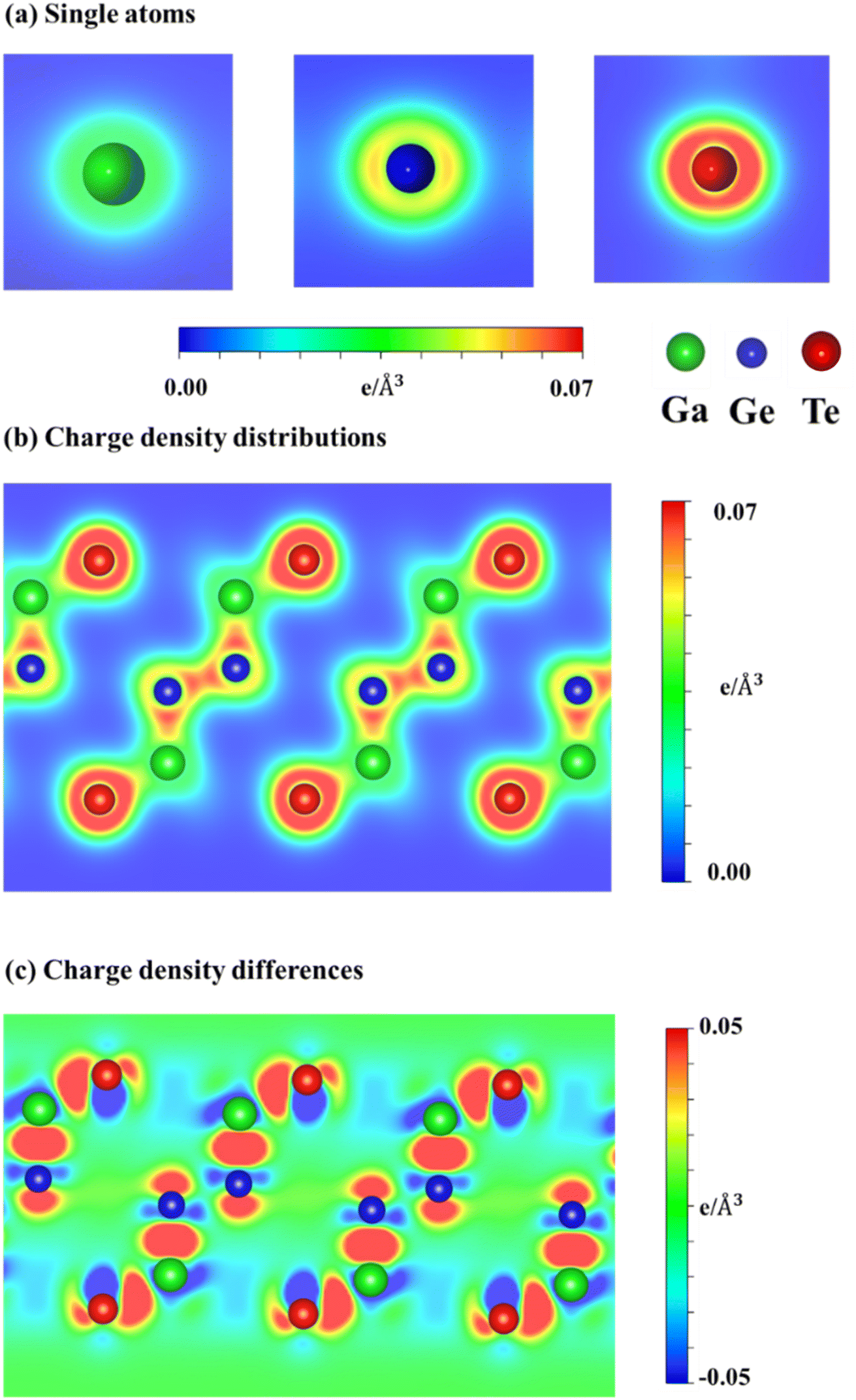 | ||
| Fig. 4 (a) Charge density distributions of single atoms, (b) charge density distributions of chemical bonds, (c) charge density differences of GaGeTe monolayer of chemical bonds. Noted: Ga, Ge, and Te atoms correspond to green, blue, and red balls. | ||
Fig. 5(a)–(d) illustrates the atom-dominated and orbital-projected density of states (DOS) of the GaGeTe monolayer, revealing a plethora of van-Hove singularities, including shoulder structures, logarithmic peaks, and asymmetric peaks. These features in the DOS originate from the parabolic, saddle-point, and constant-energy-loop energy dispersions in the band structure. The contributions of Ga, Ge, and Te atoms dominate over a wide energy range of −12.0 eV to 4.0 eV (Fig. 3(a)), confirming the presence of complex orbital hybridizations. Notably, due to differences in ionization energy, the van Hove singularities of Te orbitals mainly contribute to occupied states, while the opposite is true for Ga orbitals in unoccupied states. In terms of the orbital-projected density of states (DOS), the van Hove singularities of the Ga-/Ge-(4s, 4px, 4py, and 4pz), Te-(5s, 5px, 5py, and 5pz) orbitals exhibit significant mixing, leading to sp3–sp3 orbital hybridizations in Ge–Ge/Ga–Ge/Ga–Te chemical bonds. The disappearance of about 0.68 eV of DOS around the Fermi level (according to DFT theory) reflects the narrow indirect gap semiconductor nature of the GaGeTe monolayer (Fig. 3(a)). The interesting properties of DOS are expected to govern the optical excitations of GaGeTe monolayer, such as the threshold frequency and prominent absorption structures which are closely related to the specific orbital hybridizations.
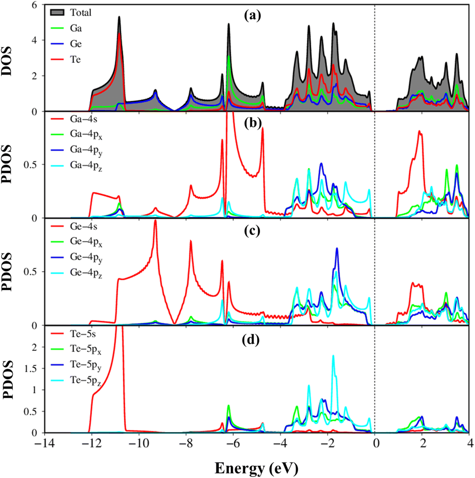 | ||
| Fig. 5 Van Hove singularities in the density of states of GaGeTe monolayer, coming to (a) Ga, Ge, Te atoms (green, blue, red curves), (b and c) Ga-/Ge-4s, 4px, 4py, 4pz orbitals (red, green, blue, and cyan curves), and (d) Te-5s, 5px, 5py, 5pz orbitals (red, green, blue, and cyan curves). | ||
To fully understand the featured properties of the GaGeTe monolayer, we also discussed its optical properties which ignore both electron–electron and electron–hole interactions. Fig. 6(a) depicts the real part ε1(ω), the imaginary part ε2(ω) of the dielectric functions of the GaGeTe monolayer, revealed by dash red and solid black curves, respectively. The optical properties of the GaGeTe monolayer are reported in the energy range of up to 10 eV. The optical gap should be larger than the band gap energy of 0.70 eV because of the conservation of momentum. In addition to the optical gap, many prominent peaks are predicted, namely P1–P5 (represented by cyan arrows). These prominence peaks are related to the vertical excitation of electrons from occupied states to unoccupied ones as can observe in Fig. 6(b). The close relationship between optical excitations and orbital hybridizations in the van Hove singularities is designated in Fig. 6(c).
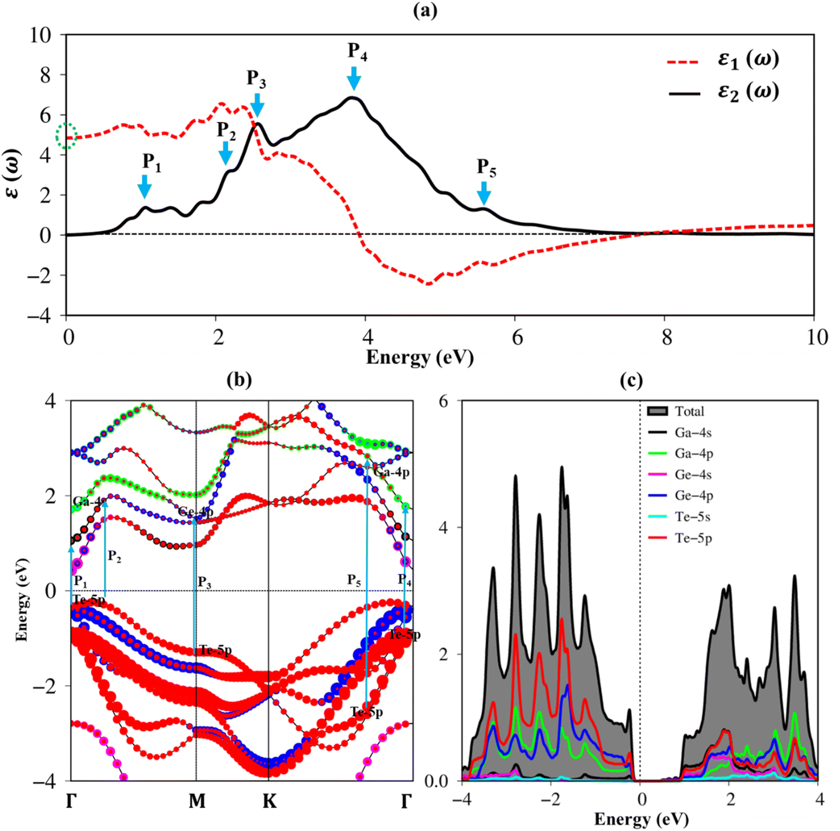 | ||
| Fig. 6 (a) The real and imaginary part of dielectric functions with prominent peaks, namely P1–P5 (cyan arrows), (b) vertical excitations from occupied states to unoccupied states (DFT standard) by using cyan arrows, corresponding to (c) transitions orbitals from occupied states to unoccupied states in van Hove singularities in the density of states. | ||
The energy loss function (ELF) as can see in Fig. 7(a) is an important parameter to predict the collective excitation of charges, and thus connect with plasma resonance. The theoretical prediction indicated that the exhibit of only one prominence plasmon mode at ωp = 8.0 eV for the polarization of EM along the in-plane direction. The purely π plasmon is similar to that of graphene is disappeared due to the significance of sp3–sp3 hybridizations.
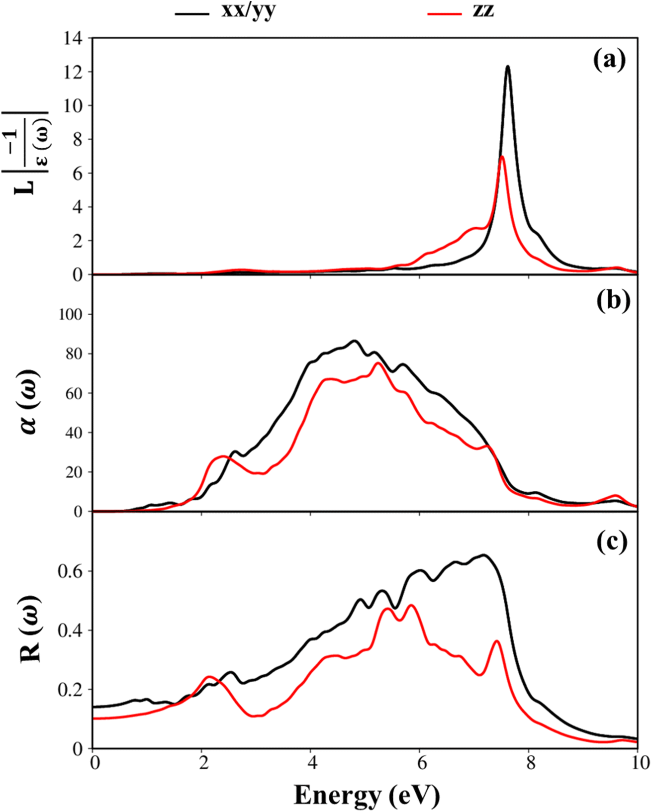 | ||
| Fig. 7 (a–c) Energy loss functions, absorbance, and reflectance spectra, respectively for GaGeTe monolayer with x-/y- (black curves) and z- (red curves) directions. | ||
In addition, Fig. 7(b) and (c) investigated the absorption α(ω), reflectance spectra R(ω) of the GaGeTe monolayer, respectively. In general, the reflectance spectra are relatively small in the solar radiation energy interval, while the average absorption coefficient value α(ω) is rather large for the GaTe monolayer,52 and thus, the GaGeTe 2D crystal is predicted to exhibit a strong absorption and weak reflectance ability in the visible spectrum.
3.2 Excitonic effects
Excitonic effects refer to the behavior of bound electron–hole pairs (excitons) through Coulomb interactions, which are fundamental concepts in solid-state physics. The presence of exciton states will play significant roles in the optical absorbance spectra, such as inducing a redshift of the optical gap, modulating the absorbance spectra, and increasing optical excitation probabilities. The optical properties of the GaGeTe monolayer systems with and without excitonic effects will be investigated in this session. Here, we used G0W0 plus BSE technique to yield a more accurate result by computing the physical effects of the electron–electron and electron–hole interactions.The imaginary part of the dielectric functions (red and black line) and the oscillator strength of the optical transitions (green bars) of the GaGeTe monolayer, imply the weakly bound nature of exciton as depicted in Fig. 8(a). In the case of the absence of excitonic effect (without electron–hole interactions), shown in the black curves, the optical gap or threshold frequency is equal to 2.30 eV which is larger than the band gap energy of 2.10 eV (GW method) due to the conservation of momentum. In addition to the optical gap, many prominent peaks appear in the imaginary part of dielectric functions. Across various levels of analysis, it was observed that the general shape of the spectra remained consistent. For comparison DFT level, the optical gap of the imaginary part of the dielectric function without excitonic effect (G0W0 level) produced a significant blue shift. In addition, the most important physical effect in the presence of excitonic effect was the appearance of some bound excitons below the band gap of GW level. In the case of the presence of excitonic effect (hole–electron interactions), showing red curves, we have two excitonic states with a very strong oscillator strength, namely E1, and E2. The two peaks appear at 1.70 eV, and 2.30 eV in the optical spectrum of the GaGeTe monolayer (see Fig. 8(a)), originating primarily from the optical transitions at the high symmetry points. Moreover, the calculated optical gap value rather matches the experimental optical gap of 1.12 eV.53
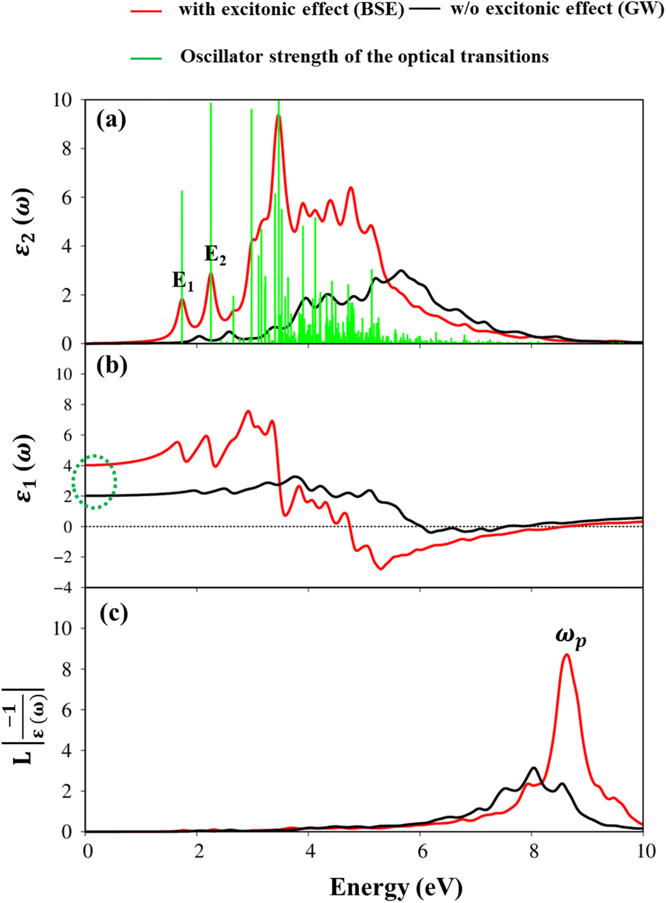 | ||
| Fig. 8 (a) The imaginary part of dielectric functions, the green lines are the oscillator strength of the optical transitions. The E1 and E2 are exciton peaks, (b) the real part of dielectric functions, as well as, (c) energy loss functions with and without excitonic effects (consider in-of-plane as an example). Noted: the red (black) curves are with (without) excitonic effects. | ||
The Kramers–Kronig relation provides a close connection between the real and imaginary components of the dielectric function, resulting in the simultaneous appearance of the pair of prominent peaks in both the real and imaginary parts. It is well known that the polarizability of a material can be estimated by the real part of the dielectric function. The static values (dashed green circles) of the real part of the complex dielectric function at ω = 0 are depicted in Fig. 8(b) are 4.0 (with excitonic effect), and 3.50 (without excitonic effect) to compare the DFT level of 4.8 (Fig. 6(a)). From the real part of the dielectric function with excitonic effect, negative values appear at ≈3.0 eV. This shows the metallic nature of the GaGeTe monolayer in the ultraviolet (UV) part of the electromagnetic spectrum. Moreover, the obtained zero-points of dielectric functions are equal to 8.60 eV (with excitonic effects). As previously indicated, one way to explain the coherent behavior of the free electrons is via the zero points in the real and imaginary parts of the dielectric functions (Fig. 8(a) and (b)). The strongest peak in ELF, as illustrated in Fig. 8(c), is about ωp = 8.60 due to almost complete un-damping of the Plasmon resonances. The Ga-/Ge-(4s, 4px, 4py, and 4pz) and Te-(5s, 5px, 5py, and 5pz) significant orbitals are responsible for this strongest peak.
Herein, we also showed the absorbance and reflectance spectra with/without excitonic effects of the GaGeTe monolayer as plotted in Fig. 9(a) and (b). Indeed, the absorption coefficient and the reflectance of solid-state materials are two general optical phenomena and reflect the principal characteristics of single and coherent excitations. As evident in Fig. 9(a), when photon energy is smaller than the onset frequency, the absorption coefficient α(ω) vanishes due to lacking electronic excitation, while the reflectance R(ω) is weakly dependent on the frequency with the reflective index is equal 0.11. However, both R(ω) and α(ω) are altering dramatically and sensitively to the excitation events above the threshold frequency. Regarding the absorption coefficient, these curves quickly increased as a result of the numerous inter-band transitions, with the Plasmon frequencies showing the most noticeable change as a result of the participation of the collective excitations. The inverse values of the absorption coefficient are between 50 Å and 100 Å for the lack and presence of the excitonic effect, respectively, showing that the abundant electronic excitations readily absorb the EM waves as they travel through the medium. On the other hand, the reflectance increases noticeably and exhibits significant variability. In the case of the presence of excitonic effect as an example, the reflectance has a 55% variation at the resonance frequency, leading to the prominence associated with the plasmon mode (ωp).
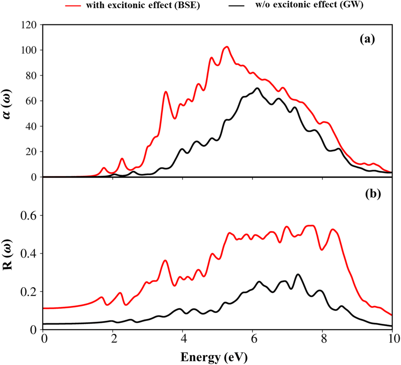 | ||
| Fig. 9 (a) The absorbance (×104 cm−1), and (b) reflectance spectra of the GaGeTe monolayer with and without excitonic effects by showing red, and black curves, respectively. | ||
4. Conclusions
In this study, according to the delicate density functional theory simulations and analyses under the atom- and orbital-decomposed quasi-particle framework, the GaGeTe monolayer exposed interesting electronic and optical properties. The GaGeTe monolayer achieved many rich-physical and chemical pictures. The diversified properties and potential application of other semiconductor materials could fully comprehend. Indeed, the GaGeTe monolayer exhibited sp3 bonds/hybridizations, a highly non-uniform/anisotropic chemical environment, the atom-dominated energy spectra within the specific energy ranges, the orbital-related charge density deformations, and the merged van Hove singularities across the Fermi level. On the other hand, the GaGeTe monolayer has buckling symmetry, characterized by the different heights of the Te–Ga–Ge–Ge–Ga–Te sequence in a unit cell. The GaGeTe monolayer possesses an indirect band gap semiconductor for 0.68 eV, 0.59 eV, 0.67 eV, and 2.16 eV of DFT, DFT + SOC, HSE, and GW levels, respectively. More importantly, the obtained results in electronic properties are associated with the optical response by orbital hybridizations in chemical bonds, including the dielectric function, energy loss function, low reflectance, and a strong absorption coefficient.In summary, the study concludes that the GaGeTe monolayer examined has wide gap semiconductor/strong excitonic effects, and low effective mass/high carrier mobility, which makes them strong candidates for the use of electronic, and optoelectronic applications. Furthermore, the examination conducted in this study can be useful for studying other graphene-like semiconductor materials and emerging materials.26,30,54–56 We encourage experimental research to verify our theoretical findings.
Conflicts of interest
The authors declare no competing interests.References
- K. S. Novoselov, A. K. Geim, S. V. Morozov, D.-e. Jiang, Y. Zhang, S. V. Dubonos, I. V. Grigorieva and A. A. Firsov, Electric field effect in atomically thin carbon films, Science, 2004, 306(5696), 666–669 CrossRef CAS PubMed.
- A. Chavez-Valdez, M. S. Shaffer and A. R. Boccaccini, Applications of graphene electrophoretic deposition. A review, J. Phys. Chem. B, 2013, 117(6), 1502–1515 CrossRef CAS PubMed.
- G. Jo, M. Choe, S. Lee, W. Park, Y. H. Kahng and T. Lee, The application of graphene as electrodes in electrical and optical devices, Nanotechnology, 2012, 23(11), 112001 CrossRef PubMed.
- D. Reddy, L. F. Register, G. D. Carpenter and S. K. Banerjee, Graphene field-effect transistors, J. Phys. D: Appl. Phys., 2011, 44(31), 313001 CrossRef.
- M. Qiao, Y. Chen, Y. Wang and Y. Li, The germanium telluride monolayer: a two dimensional semiconductor with high carrier mobility for photocatalytic water splitting, J. Mater. Chem. A, 2018, 6(9), 4119–4125 RSC.
- M. Zhou, X. Chen, M. Li and A. Du, Widely tunable and anisotropic charge carrier mobility in monolayer tin (II) selenide using biaxial strain: a first-principles study, J. Mater. Chem. C, 2017, 5(5), 1247–1254 RSC.
- W. Li, X. Qian and J. Li, Phase transitions in 2D materials, Nat. Rev. Mater., 2021, 6(9), 829–846 CrossRef CAS.
- X. Liu and M. C. Hersam, 2D materials for quantum information science, Nat. Rev. Mater., 2019, 4(10), 669–684 CrossRef.
- C. Anichini, W. Czepa, D. Pakulski, A. Aliprandi, A. Ciesielski and P. Samorì, Chemical sensing with 2D materials, Chem. Soc. Rev., 2018, 47(13), 4860–4908 RSC.
- A. Kumar and P. Ahluwalia, Mechanical strain dependent electronic and dielectric properties of two-dimensional honeycomb structures of MoX2 (X = S, Se, Te), Phys. B, 2013, 419, 66–75 CrossRef CAS.
- Y. Yin, P. Miao, Y. Zhang, J. Han, X. Zhang, Y. Gong, L. Gu, C. Xu, T. Yao and P. Xu, Significantly increased Raman enhancement on MoX2 (X = S, Se) monolayers upon phase transition, Adv. Funct. Mater., 2017, 27(16), 1606694 CrossRef.
- Z. Chen, Y. Li, K. Wang and Y. Zhang, Scalable production of intrinsic WX2 (X = S, Se, Te) quantum sheets for efficient hydrogen evolution electrocatalysis, Nanotechnology, 2021, 32(49), 495701 CrossRef CAS PubMed.
- Y. Ma, Y. Dai, M. Guo, L. Yu and B. Huang, Tunable electronic and dielectric behavior of GaS and GaSe monolayers, Phys. Chem. Chem. Phys., 2013, 15(19), 7098–7105 RSC.
- S. Suzuki, T. Iwasaki, K. K. H. De Silva, S. Suehara, K. Watanabe, T. Taniguchi, S. Moriyama, M. Yoshimura, T. Aizawa and T. Nakayama, Direct growth of germanene at interfaces between van der Waals materials and Ag (111), Adv. Funct. Mater., 2021, 31(5), 2007038 CrossRef CAS.
- N. Liu, 2D Germanene-Based Nanomaterials for Energy Applications, 2021, pp. 1–149 Search PubMed.
- W. Wang, L. Li, Z. Zhang, J. Yang, D. Tang and T. Zhai, Ultrathin GaGeTe p-type transistors, Appl. Phys. Lett., 2017, 111(20), 203504 CrossRef.
- S. R. Tamalampudi, G. Dushaq, J. E. Villegas, N. S. Rajput, B. Paredes, E. Elamurugu and M. S. Rasras, Short-wavelength infrared (SWIR) photodetector based on multi-layer 2D GaGeTe, Opt. Express, 2021, 29(24), 39395–39405 CrossRef CAS.
- B. Lv, T. Qian and H. Ding, Angle-resolved photoemission spectroscopy and its application to topological materials, Nat. Rev. Phys., 2019, 1(10), 609–626 CrossRef.
- J. Koralek, J. Douglas, N. Plumb, J. Griffith, S. Cundiff, H. Kapteyn, M. Murnane and D. Dessau, Experimental setup for low-energy laser-based angle resolved photoemission spectroscopy, Rev. Sci. Instrum., 2007, 78(5), 053905 CrossRef CAS PubMed.
- R. M. Feenstra, Scanning tunneling spectroscopy, Surf. Sci., 1994, 299, 965–979 CrossRef.
- H. J. Zandvliet and A. van Houselt, Scanning tunneling spectroscopy, Annu. Rev. Anal. Chem., 2009, 2, 37–55 CrossRef CAS PubMed.
- V. Kucek, C. Drasar, J. Navratil, L. Benes and P. Lostak, Optical and transport properties of GaGeTe single crystals, J. Cryst. Growth, 2013, 380, 72–77 CrossRef CAS.
- J. Zhang, S.-s. Li, W.-x. Ji, C.-w. Zhang, P. Li, S.-f. Zhang, P.-j. Wang and S.-s. Yan, Two-dimensional GaGeTe film: a promising graphene-like material with tunable band structure and high carrier mobility, J. Mater. Chem. C, 2017, 5(34), 8847–8853 RSC.
- C. Ke, Y. Wu, J. Zhou, Z. Wu, C. Zhang, X. Li and J. Kang, Modification of the electronic and spintronic properties of monolayer GaGeTe with a vertical electric field, J. Phys. D: Appl. Phys., 2019, 52(11), 115101 CrossRef.
- L. Xu, W. Zhou, W. Liu, X. Xia, G. Liu, T. Guo, Z. Hu, Z. Li and S. Zhang, Unexpected band gap evolution and high carrier mobility sparked by the orbital variation in two-dimensional GaGeX (X = S, Se, Te), Phys. E, 2022, 138, 115112 CrossRef CAS.
- N. Thi Han, V. Khuong Dien and M.-F. Lin, Electronic and optical properties of CsGeX3 (X = Cl, Br, and I) compounds, ACS Omega, 2022, 7(29), 25210–25218 CrossRef CAS PubMed.
- N. T. Han, V. K. Dien and M.-F. Lin, Excitonic effects in the optical spectra of Li2SiO3 compound, Sci. Rep., 2021, 11(1), 7683 CrossRef CAS PubMed.
- V. K. Dien, W.-B. Li, K.-I. Lin, N. T. Han and M.-F. Lin, Electronic and optical properties of graphene, silicene, germanene, and their semi-hydrogenated systems, RSC Adv., 2022, 12(54), 34851–34865 RSC.
- N. T. Han, V. K. Dien, N. T. T. Tran, D. K. Nguyen, W.-P. Su and M.-F. Lin, First-principles studies of electronic properties in lithium metasilicate (Li2SiO3), RSC Adv., 2020, 10(41), 24721–24729 RSC.
- N. T. Han, V. K. Dien and M.-F. Lin, Electronic and optical properties of CH3NH3SnI3 and CH(NH2)2SnI3 perovskite solar Cell, Phys. Status Solidi RRL, 2023, 2300020 CrossRef CAS.
- K. Burke, Perspective on density functional theory, J. Chem. Phys., 2012, 136(15), 150901 CrossRef.
- J. Hafner, Ab initio simulations of materials using VASP: Density-functional theory and beyond, J. Comput. Chem., 2008, 29(13), 2044–2078 CrossRef CAS PubMed.
- J. P. Perdew, K. Burke and Y. Wang, Generalized gradient approximation for the exchange-correlation hole of a many-electron system, Phys. Rev. B: Condens. Matter Mater. Phys., 1996, 54(23), 16533 CrossRef CAS PubMed.
- H. Peng and J. P. Perdew, Rehabilitation of the Perdew-Burke-Ernzerhof generalized gradient approximation for layered materials, Phys. Rev. B, 2017, 95(8), 081105 CrossRef.
- G. K. Madsen, Functional form of the generalized gradient approximation for exchange: The PBE α functional, Phys. Rev. B: Condens. Matter Mater. Phys., 2007, 75(19), 195108 CrossRef.
- S. N. Maximoff, M. Ernzerhof and G. E. Scuseria, Current-dependent extension of the Perdew–Burke–Ernzerhof exchange-correlation functional, J. Chem. Phys., 2004, 120(5), 2105–2109 CrossRef CAS PubMed.
- P. E. Blöchl, Projector augmented-wave method, Phys. Rev. B: Condens. Matter Mater. Phys., 1994, 50(24), 17953 CrossRef PubMed.
- D. J. Chadi and M. L. Cohen, Special points in the Brillouin zone, Phys. Rev. B: Solid State, 1973, 8(12), 5747 CrossRef.
- J. Heyd, J. E. Peralta, G. E. Scuseria and R. L. Martin, Energy band gaps and lattice parameters evaluated with the Heyd-Scuseria-Ernzerhof screened hybrid functional, J. Chem. Phys., 2005, 123(17), 174101 CrossRef.
- A. Togo, First-principles Phonon Calculations with Phonopy and Phono3py, J. Phys. Soc. Jpn., 2023, 92(1), 012001 CrossRef.
- G. Pizzi, V. Vitale, R. Arita, S. Blügel, F. Freimuth, G. Géranton, M. Gibertini, D. Gresch, C. Johnson and T. Koretsune, Wannier90 as a community code: new features and applications, J. Phys.: Condens. Matter, 2020, 32(16), 165902 CrossRef CAS PubMed.
- A. Crépieux and P. Bruno, Theory of the anomalous Hall effect from the Kubo formula and the Dirac equation, Phys. Rev. B: Condens. Matter Mater. Phys., 2001, 64(1), 014416 CrossRef.
- J. Vinson, J. Rehr, J. Kas and E. Shirley, Bethe-Salpeter equation calculations of core excitation spectra, Phys. Rev. B: Condens. Matter Mater. Phys., 2011, 83(11), 115106 CrossRef PubMed.
- T. Nagatomi, R. Shimizu and R. Ritchie, Energy loss functions for electron energy loss spectroscopy, Surf. Sci., 1999, 419(2–3), 158–173 CrossRef CAS.
- S.-I. Thomasson, On the absorption coefficient, Acta Acust. Acust., 1980, 44(4), 265–273 Search PubMed.
- S. Mallick and L. N. Frazer, Practical aspects of reflectivity modeling, Geophysics, 1987, 52(10), 1355–1364 CrossRef.
- R. Lin, D. Zhao, J. Zhang, H. Cao, J. Zeng, X. Wang, W. Bai, J. Yang, Y. Zhang and X. Tang, Thickness-dependent semimetal-to-semiconductor transition in two-dimensional GaGeTe, J. Appl. Phys., 2023, 133(2), 024304 CrossRef CAS.
- A. Taheri, S. Pisana and C. V. Singh, Importance of quadratic dispersion in acoustic flexural phonons for thermal transport of two-dimensional materials, Phys. Rev. B, 2021, 103(23), 235426 CrossRef CAS.
- F. Giustino, M. L. Cohen and S. G. Louie, GW method with the self-consistent Sternheimer equation, Phys. Rev. B: Condens. Matter Mater. Phys., 2010, 81(11), 115105 CrossRef.
- J. Lischner, D. Vigil-Fowler and S. G. Louie, Physical origin of satellites in photoemission of doped graphene: An ab initio G W plus cumulant study, Phys. Rev. Lett., 2013, 110(14), 146801 CrossRef.
- A. Malashevich, M. Jain and S. G. Louie, First-principles DFT+ G W study of oxygen vacancies in rutile TiO2, Phys. Rev. B: Condens. Matter Mater. Phys., 2014, 89(7), 075205 CrossRef.
- S. Demirci, N. Avazlı, E. Durgun and S. Cahangirov, Structural and electronic properties of monolayer group III monochalcogenides, Phys. Rev. B, 2017, 95(11), 115409 CrossRef.
- E. Haubold, A. Fedorov, F. Pielnhofer, I. P. Rusinov, T. V. Menshchikova, V. Duppel, D. Friedrich, R. Weihrich, A. Pfitzner and A. Zeugner, Possible experimental realization of a basic Z 2 topological semimetal in GaGeTe, APL Mater., 2019, 7(12), 121106 CrossRef.
- H. Sun, S.-S. Li, W.-x. Ji and C.-W. Zhang, Valley-dependent topological phase transition and quantum anomalous valley Hall effect in single-layer RuClBr, Phys. Rev. B, 2022, 105(19), 195112 CrossRef CAS.
- Y.-t. Han, W.-x. Ji, P.-J. Wang, P. Li and C.-W. Zhang, Strain-tunable skyrmions in two-dimensional monolayer Janus magnets, Nanoscale, 2023, 15(14), 6830–6837 RSC.
- S.-j. Zhang, C.-w. Zhang, S.-f. Zhang, W.-x. Ji, P. Li, P.-j. Wang, S.-s. Li and S.-s. Yan, Intrinsic Dirac half-metal and quantum anomalous Hall phase in a hexagonal metal-oxide lattice, Phys. Rev. B, 2017, 96(20), 205433 CrossRef.
| This journal is © The Royal Society of Chemistry 2023 |