
 Open Access Article
 This Open Access Article is licensed under a Creative Commons Attribution-Non Commercial 3.0 Unported Licence
Metal organic framework derived NiOx nanoparticles for application as a hole transport layer in perovskite solar cells
Md. Ariful Islama,
Vidhya Selvanathan*f,
Puvaneswaran Chelvanathana,
M. Mottakinab,
Mohammod Aminuzzamanc,
Mohd Adib Ibrahim a,
Ghulam Muhammadd and
Md. Akhtaruzzaman*ae
a,
Ghulam Muhammadd and
Md. Akhtaruzzaman*ae
aSolar Energy Research Institute (SERI), Universiti Kebangsaan Malaysia (UKM), 43600 Bangi, Selangor, Malaysia. E-mail: akhtar@ukm.edu.my
bDepartment of Applied Chemistry and Chemical Engineering, Bangabandhu Sheikh Mujibur Rahman Science and Technology University, Gopalganj-8100, Bangladesh
cDepartment of Chemical Science, Faculty of Science, Universiti Tunku Abdul Rahman (UTAR), Perak Campus, Jalan Universiti, Bandar Barat, 31900 Kampar, Perak D. R., Malaysia
dDepartment of Computer Engineering, College of Computer and Information Sciences, King Saud University, Riyadh, Saudi Arabia
eGraduate School of Pure and Applied Sciences, University of Tsukuba, Tsukuba, Ibaraki 305-8573, Japan
fInstitute of Sustainable Energy, Universiti Tenaga Nasional (The Energy University), Jalan Ikram-Uniten, Kajang 43000, Selangor, Malaysia
First published on 27th April 2023
Abstract
NiOx as a hole transport layer (HTL) has gained a lot of research interest in perovskite solar cells (PSCs), owing to its high optical transmittance, high power conversion efficiency, wide band-gap and ease of fabrication. In this work, four different nickel based-metal organic frameworks (MOFs) using 1,3,5-benzenetricarboxylic acid (BTC), terephthalic acid (TPA), 2-aminoterephthalic acid (ATPA), and 2,5-dihydroxyterephthalic acid (DHTPA) ligands respectively, have been employed as precursors to synthesize NiOx NPs. The employment of different ligands was found to result in NiOx NPs with different structural, optical and morphological properties. The impact of calcination temperatures of the MOFs was also studied and according to field emission scanning electron microscopy (FESEM), all MOF-derived NiOx NPs exhibited lower particle size at lower calcination temperature. Upon optimization, Ni-TPA MOF derived NiOx NPs calcined at 600 °C were identified to be the best for hole transport layer application. To explore the photovoltaic performance, these NiOx NPs have been fabricated as a thin film and its structural, optical and electrical characteristics were analyzed. According to the findings, the band energy gap (Eg) of the fabricated thin film has been found to be 3.25 eV and the carrier concentration, hole mobility and resistivity were also measured to be 6.8 × 1014 cm−3; 4.7 × 10¹⁴ Ω cm and 2.0 cm2 V−1 s−1, respectively. Finally, a numerical simulation was conducted using SCAPS-1D incorporating the optical and electrical parameters from the thin film analysis. FTO/TiO2/CsPbBr3/NiOx/C has been utilized as the device configuration which recorded an efficiency of 13.9% with Voc of 1.89 V, Jsc of 11.07 mA cm−2, and FF of 66.6%.
1 Introduction
Metal oxide nanostructures possess numerous unique features that become distinct from those present in the bulk solid state due to their size differences. Particle size reduction in the nanoscale domain offers a variety of unique characteristics, including low sintering temperature, large specific surface area and quantum size effect.1 Out of all the metal oxides, NiOx nano-structures have received substantial scientific interest owing to their high band gaps (3.6–4.0 eV) and p-type electrical conductivity characteristics.2 Moreover, NiOx nanoparticles (NPs) offer a number of applications including in battery cathodes,3 as catalysis,4 electrodes of fuel cells, in the field of electrochromic films,5 gas sensors6 and magnetic materials.7 Additionally, NiOx NPs are also being used in smart windows,8 as the effective hole transporting layer (HTL) in PSCs,9 dye-sensitized photocathodes10 and electrochemical supercapacitors.11 As a hole transport layer (HTL), NiOx is very promising for PSCs because of its deep valence band, affordable cost, high optical transmittance and outstanding stability.12,13 Recently, a number of experiments have been conducted on NiOx-based PSCs to make the device more reliable and efficient. In order to generate a uniform and homogenous thin film, Pei-Huan Lee et al. conducted an emulsion process to synthesize NiOx NPs. Using this thin film, they achieved a PCE of 18%.13 Shuangjie Wang et al. applied an ionic liquid (NiOx-IL) during the synthesis process and they found a promising PCE of 22.62%.14 The structural, electrical, optical, compositional and magnetic properties of NiOx NPs are highly dependent on the synthesis process, particle size and shape. Generally, the experimental route adopted for the synthesis of NiOx NPs is very crucial in governing a number of key factors, including crystallinity, size and shape, composition-purity of the final product.15 So far, in comparison to other conventional methods like spray-pyrolysis, co-precipitation, sol–gel, microwave pyrolysis, thermal decomposition; solvothermal is an efficient and simple technique for the synthesis of NPs because it offers comparatively large specific surface area with low temperature processing step.16 Solvothermal technique has successfully overcome challenges such as utilization of expensive specialized equipment, low energy usage, high purity and large-scale manufacturing.16 Considering all of these, much effort has been devoted in recent past to the development of metal–organic frameworks (MOFs) as precursors utilized in the synthesis process of porous oxides. Basically, MOFs are defined as porous hybrid compound, that consist of metal ions which are connected with organic ligands via coordination bond and create a three-dimensional framework.17,18 In comparison, MOFs offer a wider range of options to design and construct the hierarchically nanostructures, a class of polyfunctional compounds with a number of morphological and topological characteristics.19Most studies have stated that the morphology and size of particles of the metal oxides derived from MOF depends on the chemical structure of the ligand used which in turn, tunes the overall architecture. Typically for any NP synthesis, the homogeneity, NPs shape and size can be tuned by changing the solution concentration, pH, nucleation rate, reaction temperature and presence of complexing agent in the synthesis process.20 Among these factors, calcination temperature is very important because it alters the shape and morphological properties of nanoparticles as well as creating defects, which leads to the formation of new energy state.21 The phase of the materials is often influenced by the sintering temperature, which in turn affects the materials' structural and optical properties.21 So, its highly necessary to calcine the produced nanoparticles at elevated temperatures in order to obtain single phase nanostructures of the right size.20 The removal of impure phases, and an improvement in particle density and a rise in crystallites are some potential benefits of this step.20 For synthesis of MOF derived NPs, it is essential to ensure the calcination temperature is high enough to produce high purity metal oxides while at the same time ensure particles with desired size and shape is produced.
This article addressed the synthesis process of NiOx NPs derived from metal–organic framework by utilizing four distinct ligands namely 1,3,5-benzenetricarboxylic acid (BTC), terephthalic acid (TPA), 2-aminoterephthalic acid (ATPA), 2,5-dihydroxyterephthalic acid (DHTPA). The effect of different ligand structure of the MOF precursors calcined at different temperature on the structural, morphological and optical properties of the synthesized NiOx NPs was analyzed. In extension the MOF derived NPs were applied as potential hole transport layer (HTL) in n-i-p PSCs to elucidate the future potential as component in energy storage devices.
2 Materials and methods
2.1 Materials
All chemicals and reagents were utilized, without additional purification. Ni(NO3)2·6H2O; 1,3,5-benzenetricarboxylic acid (BTC), terephthalic acid (TPA), 2-aminoterephthalic acid (ATPA), 2,5-dihydroxyterephthalic acid (DHTPA), dimethylformamide (DMF), ethanol, KOH, methanol, acetone, absolute ethanol (99.9%), acetic acid, ethylene glycol, 1-ethyl-3-methylimidazolium tetrafluoroborate, fluorine doped tin oxide (FTO) coated soda-lime glass substrate (SLG), were pursed from Sigma Aldrich, Germany.2.2 Synthesis of MOF derived NiOx NPs
The MOF-derived NiOx NPs were synthesized by solvothermal method (Fig. 1). For this experiment, 2.1 mmol Ni(NO3)2·6H2O and 3 mmol ligand (BTC/TPA/ATPA/DHTPA) were well dispersed in 15 mL dimethylformamide (DMF). The resulting dispersed solutions were placed in 100 mL Teflon-polytetrafluoroethylene coated autoclave with stainless steel jacket at 160 °C for 12 h. After completing the reaction, the colloidal solutions were taken out from autoclave and left it for cooling down to ambient temperature naturally. After centrifuging the colloidal solution, it was repeatedly rinsed with ethanol and water for 3 times. Then the colloidal solutions were centrifuged and rinsed with ethanol and water for several time. The products were dried in an oven at 80 °C for 8 h to obtain MOFs. Finally, these Ni-MOFs were calcined in a furnace for 5 hours at different temperature (600 °C, 700 °C, and 900 °C) to achieve the desired NiOx nanoparticles.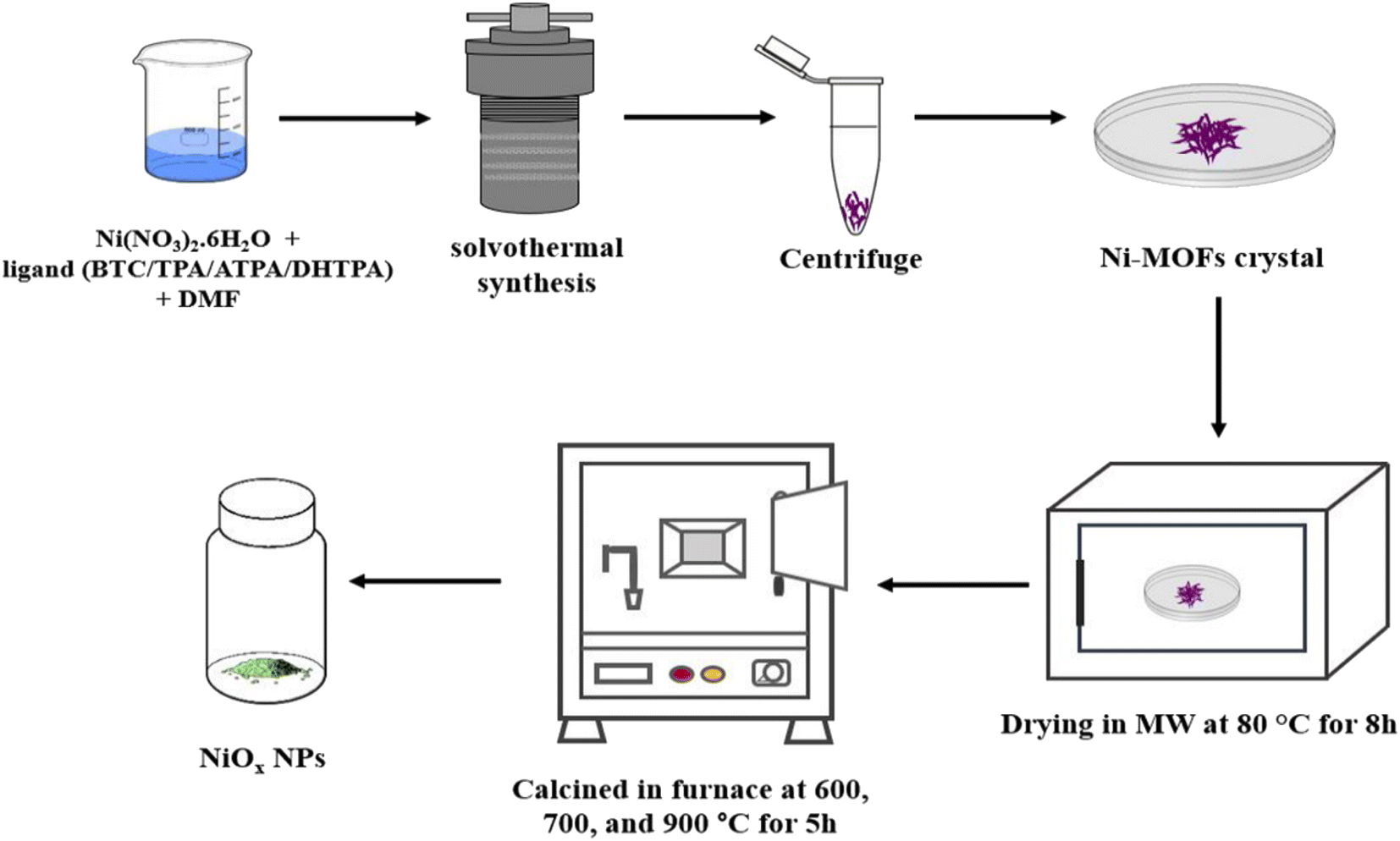 | ||
| Fig. 1 Synthesis process of MOF-derived NiOx NPs. | ||
2.3 Fabrication of NiOx thin film
Bare SLG and FTO coated SLG were used as a substrate for the deposition of NiOx thin films. Bare SLG has been utilized to measure the thin film's electrical characteristics, while FTO coated SLG was used to evaluate the film's structural and optical characteristics. The substrates were cleaned by using an ultrasonic cleaner with ethanol, acetone, and DI water; afterwards dried with a stream of N2 gas. Prior to spin coating, all substrates were treated for 15 min with UV-ozone plasma. NiOx colloidal dispersion was prepared by dissolving 40 mg NiOx synthesized powder into 2 mL absolute ethanol with the concentration of 20 mg mL−1 30 μL acetic acid, 150 μL ethylene glycol and 500 μL ionic liquid (BMIMBF4) have also been incorporated to make a homogenous dispersion. The dispersion was subsequently coated onto the glass substrate with the speed of 4000 rpm for 30 s, followed by 10 min of baking at 200 °C on a hot plate. Finally, the films calcined at 300 °C for 1 h into a furnace. All of these operations were performed under ambient conditions.2.4 Nanoparticles and thin film characterization
The morphological and structural characteristics of MOF-derived NiOx NPs and thin film were carried out by using several characterization approaches such as X-ray diffraction (XRD), field emission scanning electron microscope (FeSEM), absorption spectra (UV-Vis) coupled with Fourier transform infrared (FTIR). The XRD were measured in the 2θ with a region of 10° to 90° for NPs and 10° to 80° for thin film respectively utilizing an X-ray diffractometer ‘BRUKER aXS-D8 Advance Cu-Ka'. For the detection of functional group, Bruker FTIR spectrometer has been used with spectral range from 4000 to 500 cm−1. To investigate the grain size, surface morphology and growth of NPs FeSEM model ‘LEO 1450 VP’ was utilized. UV-Vis spectrophotometer PerkinElmer Lambda 35 was being used to evaluate optoelectronic characteristics, including optical absorbance and transmittance. The electrical characteristics of thin film were measured, using the HMS ECOPIA 3000 Hall effect measuring system under a magnetic field (0.57 T).3 Results and discussion
3.1 Properties of MOF derived NiOx nanoparticle
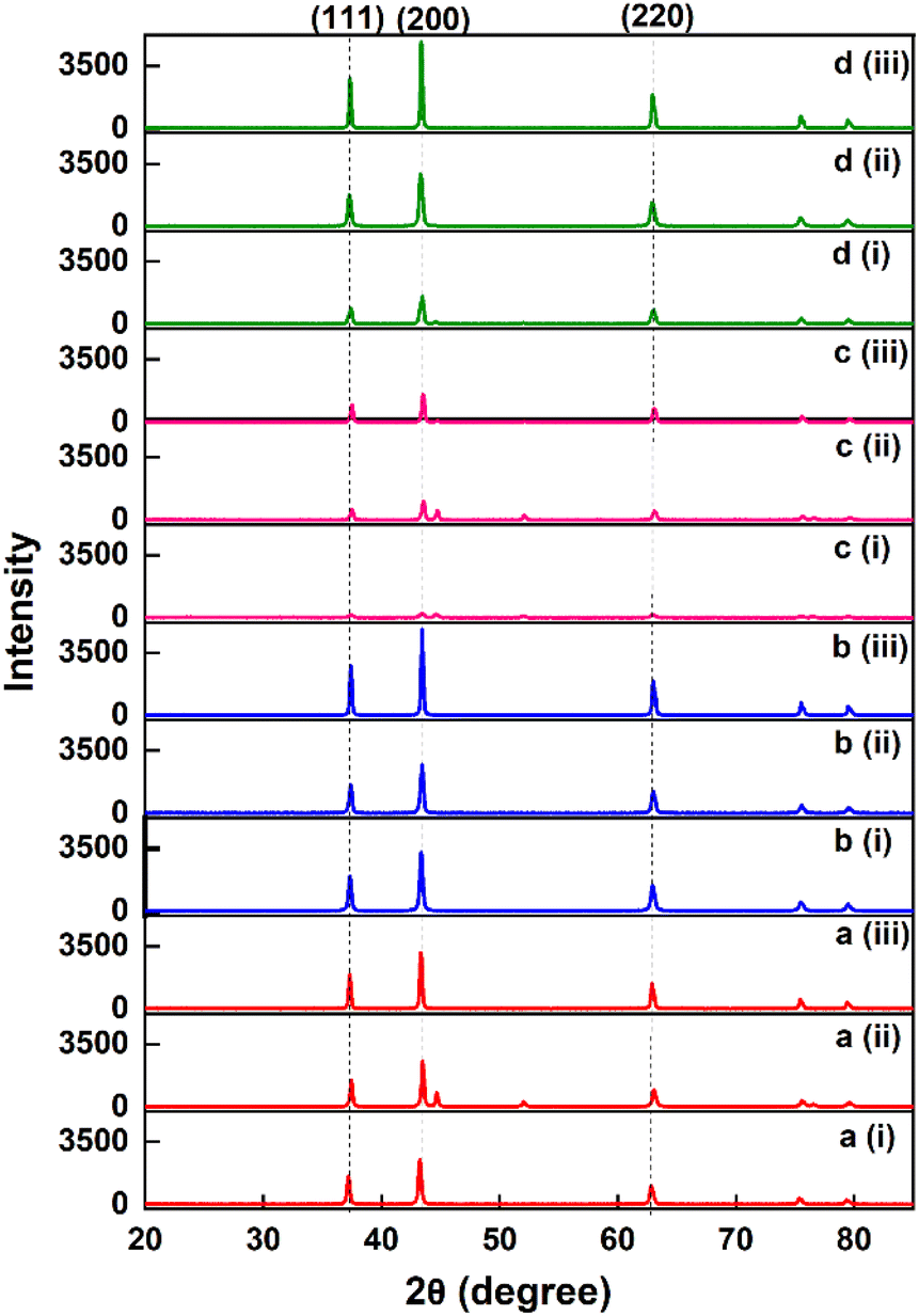 | ||
| Fig. 2 X-ray diffractogram of MOF-derived NiOx nanoparticles (a) NiOx-BTC (b) NiOx-TPA (c) NiOx-ATPA and (d) NiOx-DHTPA mediated calcined at (i) 600 °C and (ii) 700 °C (iii) 900 °C. | ||
Highly pure NiOx can be obtained with high sintering temperature (900 °C), result in sharp peak intensity. NiOx-BTC (700 °C); NiOx-ATPA (600 °C and 700 °C); and NiOx-DHTPA (600 °C), all exhibit two faint peaks at 2θ with the value of around 44.8° and 51.7° due to impurities in the synthesized powder. With the help of Scherer's formula, the average crystal sizes (D) were determined:24
 | (1) |
Table 1 shows that crystallite size increases along with a rise in sintering temperature. At higher heat treatment, particles imperfections, edges and flaws are removed, resulting in large size crystallites with definite crystalline phase.25
| Material | Calcination temperature (°C) | Average crystallite size (nm) | Average strain (ε) |
|---|---|---|---|
| NiOx-BTC | 600 | 24.77 | 0.0029 |
| 700 | 25.69 | 0.0029 | |
| 900 | 29.54 | 0.0025 | |
| NiOx-TPA | 600 | 23.79 | 0.0030 |
| 700 | 24.34 | 0.0030 | |
| 900 | 30.81 | 0.0023 | |
| NiOx-ATPA | 600 | 20.60 | 0.0037 |
| 700 | 22.20 | 0.0027 | |
| 900 | 28.03 | 0.0026 | |
| NiOx-DHTPA | 600 | 21.90 | 0.0033 |
| 700 | 22.27 | 0.0033 | |
| 900 | 31.39 | 0.0023 |
Furthermore, peak stretching or broadening is relayed to the quantum confinement and lattice strain effect of NPs because of its large crystallite size and grain boundaries, respectively. To investigate the influence of strain on the structural characteristics of NiOx nanoparticles, Williamson Hall (W–H) analysis is introduced. The W–H equation is represented as26
 | (2) |
Table 1 further demonstrates the relation between strain and crystallite size of NiOx NPs. It has been observed that the strain reduces as the size of the crystallites increase. The reason for this behavior is the possibility of impurities and defects in NPs and also the surface area is vast in contrast.26 Therefore, XRD indicates that NiOx-TPA (900 °C) and NiOx-DHTPA (900 °C) has the least strain value approximately 0.0023, compared to other NPs, indicating that they are highly crystalline with less structural flaws.
Fig. 3 illustrates the FTIR absorption spectra of all synthesized Ni-MOFs and their corresponding NPs. FTIR study of Ni-BTC MOF has been described in Fig. 3a. The formation of Ni-BTC MOFs has been confirmed by obtaining a significant shift in the carbonyl (–CO–) groups at 1608 cm−1, suggesting that the ligand's carboxylate moieties have been deprotonated and coordinated with Ni2+. Moreover, the Ni–O stretching vibration is characterized by a strong absorption spectrum at 724 cm−1. O–H stretching was found as a wideband at 2800–3500 cm−1, suggesting the coordinated water molecule in Ni-BTC MOF prior to activation.27 Fig. 3b depicts the FT-IR spectra of the Ni-TPA metal–organic framework. As shown in Fig. 3b, Ni-TPA MOF exhibits two prominent peaks at around 1380 cm−1 and 1580 cm−1 accordingly, which are due to the symmetric and asymmetric stretching of ligand's carboxyl (–COO−) group. Separating the stretching modes indicated that TPA ligand's –COOH groups were linked to Ni2+ ions through a bidentate binding manner.28 Narrow and weak bands at 1025 cm−1 is owing to the stretching (C–H) and bending (C–H) of aromatic ring, which indicating the presence of organic ligand in the MOF. The wide peaks in between 3400–3600 cm−1 may be attributed owing to acidic –OH or crystal water.29 Investigation of the FTIR spectra of Ni-ATPA MOF as shown in Fig. 3c, indicating –NH2 stretching vibration at around 3308 cm−1. The absorption peaks at around 1387–1689 cm−1 may be detected owing to symmetric and asymmetric stretching vibrations of the –COOH groups. Moreover, O–Ni–O vibrational peaks had been found at 530 cm−1 and 668 cm−1 in respective Ni-ATPA MOF, indicating the establishment of the coordination bonding among the –COOH groups from ATPA and Ni2+.30 For the Ni-DHTPA, the benzene rings out-of-plane vibrational peak detected at around 888 cm−1 (Fig. 3d). For carboxylate groups, symmetric and asymmetric stretching appears at around 1410 cm−1 and 1556 cm−1. The interlayer water and C–O–H contribute to the wide band at 3425 cm−1. This implies that Ni2+ has been effectively coordinated with DHTPA ligand.31,32
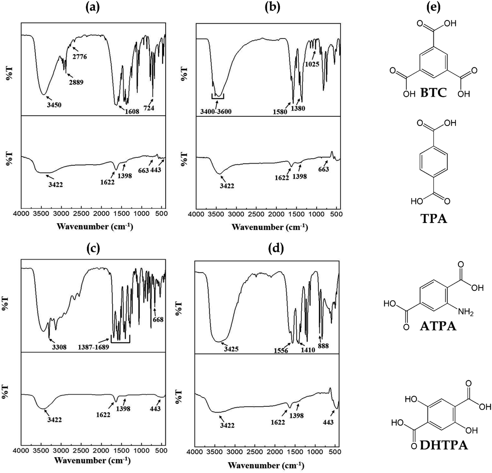 | ||
| Fig. 3 FTIR spectral absorption of synthesized Ni-MOFs and its corresponding NiOx NPs (a) Ni-BTC (b) Ni-TPA (c) Ni-ATPA (d) Ni-DHTPA and (e) the chemical structures of ligands. | ||
In respect of FTIR spectra study, all NiOx-MOF derived NPs showed the absorption in similar region and there were no traces of peaks attributed to ligands in the MOF. This observation verifies that the Ni-MOF structures were completely transformed into NiOx upon calcination even at 600 °C. It has been observed that, O–Ni–O vibrations are responsible for the FTIR spectrum peak about 663 and 443 cm−1. Furthermore, the wide peak at 1398, 3422 and 1622 cm−1 can be ascribed to stretching and bending vibration of the hydroxyl group captured on the surface of the catalyst from the environment during FTIR examination. The symmetric and asymmetric stretching of C–O and O–C![[double bond, length as m-dash]](https://www.rsc.org/images/entities/char_e001.gif) O may also be appeared with a narrow band intensity with the range between 1000–1500 cm−1 that indicating a strong physical absorption to CO2 and H2O.23,33
O may also be appeared with a narrow band intensity with the range between 1000–1500 cm−1 that indicating a strong physical absorption to CO2 and H2O.23,33
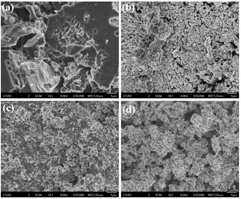 | ||
| Fig. 4 FeSEM image of (a) Ni-BTC MOF and corresponding NiOx NPs calcined at (b) 600 °C (c) 700 °C (d) 900 °C. | ||
SEM observations of the Ni-TPA MOF and relevant NPs at various sintering temperatures as illustrated in Fig. 5. Ni-TPA MOF showed hierarchical plate-like structure (Fig. 5a). NPs seem to be more compact, uniform-sized, and spherical in shape when MOF is treated at 600 °C (Fig. 5b). The well-defined nanostructures are also observed at 700 °C but the particles size is bigger than at 600 °C (Fig. 5c). For 700 °C, the nanoparticles size varied with ranging from 40 to 95 nm, whereas at 600 °C in between 25–50 nm. Particles at 900 °C have high crystallites with a spherical form, having particle sizes ranging from 85 to 130 nm (Fig. 5d).
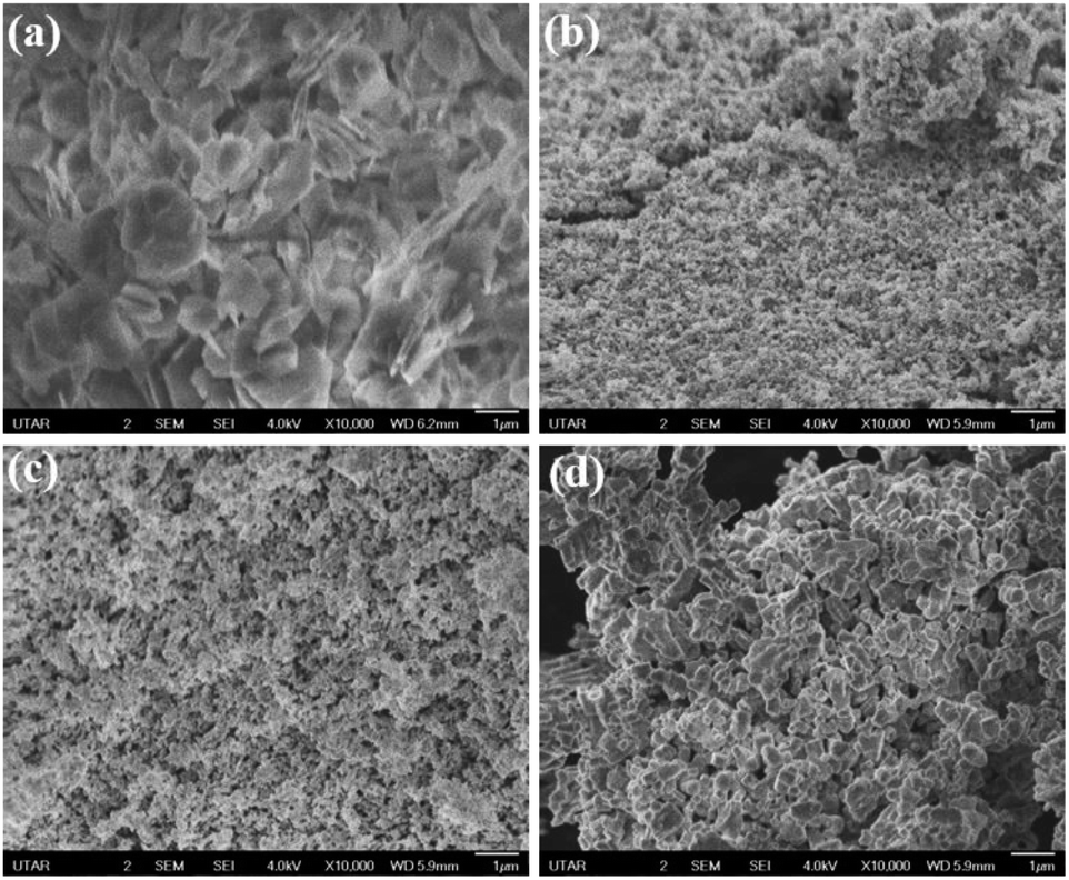 | ||
| Fig. 5 FeSEM image of (a) Ni-TPA MOF and corresponding NiOx NPs calcined at (b) 600 °C (c) 700 °C (d) 900 °C. | ||
With different calcination temperature, NiOx NPs derived from Ni-ATPA MOF exhibit the most morphological changes as shown in Fig. 6. For Ni-ATPA MOF hierarchical plate-like structure was obtained as like as Ni-TPA MOF (Fig. 6a). It has been observed that at 600 °C, the NPs are highly agglomerated and take on a spherical shape (Fig. 6b). The structure of the particle changes into a very compact reticular shape at 700 °C (Fig. 6c). Whereas at 900 °C, a quasi-cubic NPs structure has been identified (Fig. 6d).
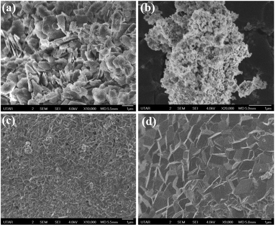 | ||
| Fig. 6 FeSEM image of (a) Ni-ATPA MOF and corresponding NiOx NPs calcined at (b) 600 °C (c) 700 °C (d) 900 °C. | ||
The FeSEM image of Ni-DHTPA MOF also depicted a plate like structure (Fig. 7a). The NiOx nanoparticles exhibited an irregular shaped crystal structure for all sintering temperature; however, particle size and crystallinity improve with increasing temperatures (Fig. 7b–d).
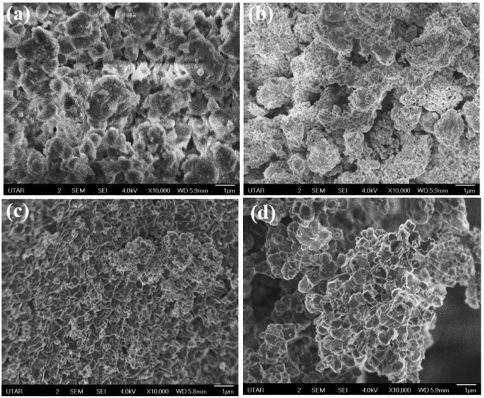 | ||
| Fig. 7 FeSEM image of (a) Ni-DHTPA MOF and corresponding NiOx NPs calcined at (b) 600 °C (c) 700 °C (d) 900 °C. | ||
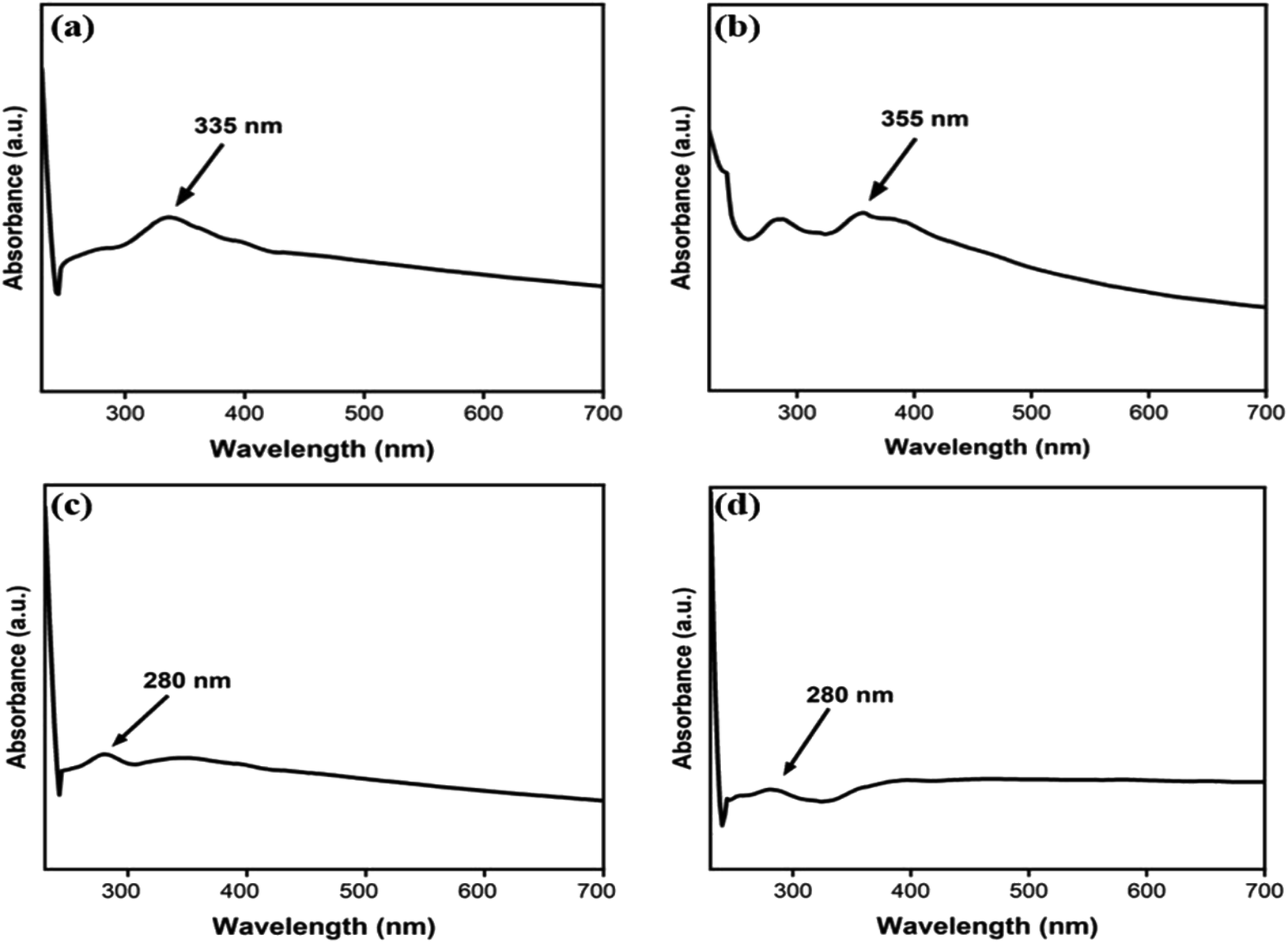 | ||
| Fig. 8 UV-Visible spectra (a) NiOx-BTC (b) NiOx-TPA (c) NiOx-ATPA (d) NiOx-DHTPA nanoparticles. | ||
3.2 MOF derived NiOx thin film as a potential hole transport layer (HTL) in perovskite solar cell
For the fabrication of NiOx thin film as hole transport layer, it is important to ensure the material has small particle size with homogeneous distribution. Based on morphological properties discussed in previous section, TPA-derived NiOx NPs calcined at 600 °C was selected for fabrication of NiOx thin film. Fig. 9a depicts the XRD analysis of the NiOx film deposited on the top of the FTO. The diffraction intensity for the NiOx thin film have been detected at 2θ with the value of 37.0°, 43.2°, and 62.8°, which correspond to the crystallographic plane of (111), (200), and (220), respectively [JCPDS No. 73-1519]. The obtained patterns suggest a cubic phase structure, which is consistent with earlier findings.38 The percentage of transmittance spectra for NiOx thin film has been shown in Fig. 9b. In the visible spectrum region, the film had a high degree of transmittance with the values above 70% for the wavelength of 400 nm to 550 nm. The band gap (Eg) of the thin film was calculated using Tauc plot, as shown in Fig. 9c, and found to be approximately 3.25 eV. The following equation has been employed to calculate the value of Eg:39
 | (3) |
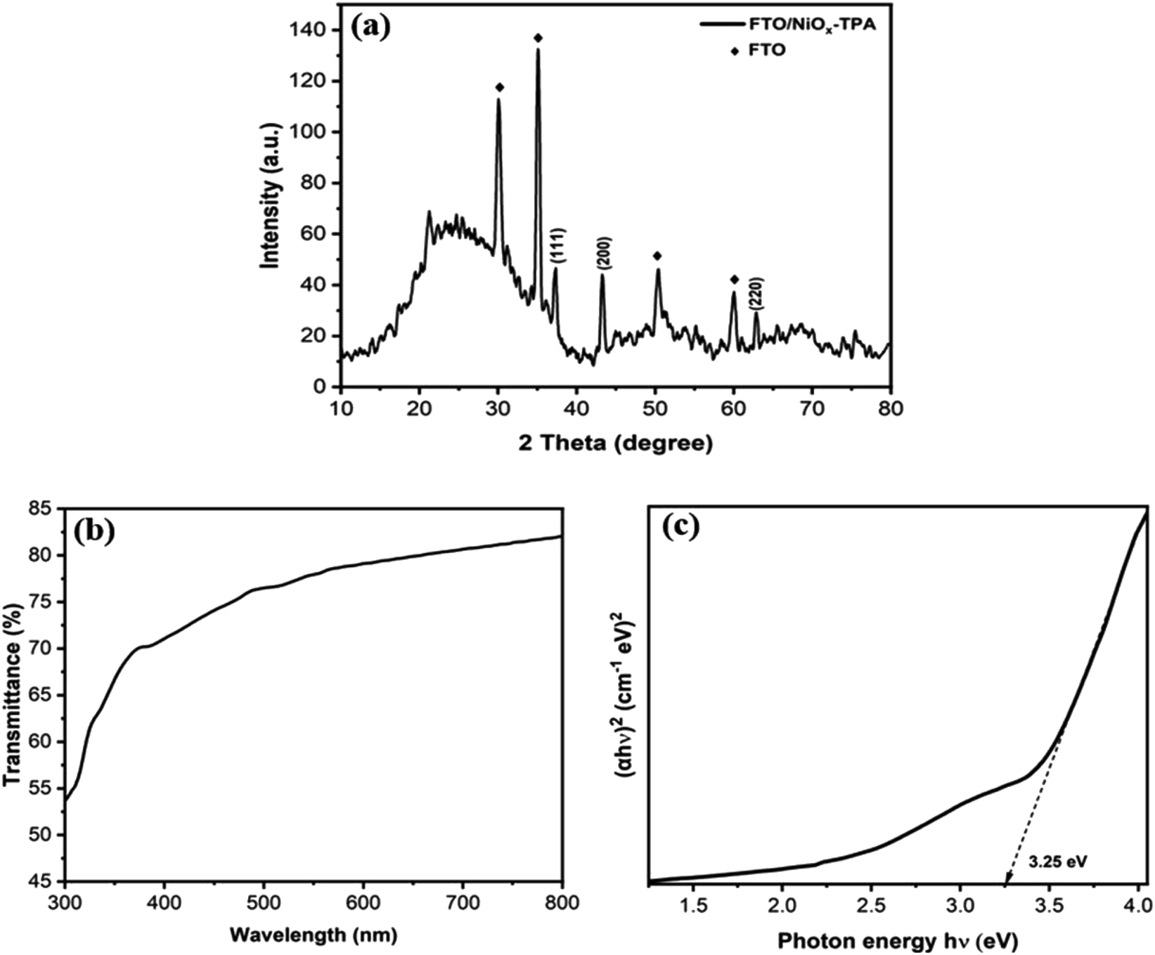 | ||
| Fig. 9 Deposited NiOx thin film's (a) XRD spectrum, (b) % of transmittance (c) Tauc plot. | ||
Furthermore, Hall measurements were conducted to determine the carrier concentration, mobility, and resistivity of the deposited thin film. Table 2 represents the findings.
| Carrier concentration (cm−3) | Resistivity (Ω cm) | Hole mobility (cm2 V−1 s−1) |
|---|---|---|
| 6.8 × 10¹⁴ (p-type) | 4.69 × 10³ | 2 |
To evaluate the photovoltaic performance of TPA derived NiOx thin film, a simulation was performed by using the SCAPS-1D software with a standard spectrum of AM1.5 G (1000 W m−2; T = 300 K) for illumination. In this simulation, synthesized NiOx-TPA (600 °C) has been used as a hole transport layer (HTL) and TiO2 (Eg = 3.2 eV) as an electron transport layer (ETL). CsPbBr3 employed as a perovskite with a band gap of 3.6 eV. The suggested device architecture of (FTO/TiO2/CsPbBr3/NiOx/C) has been depicted schematically in Fig. 10a. Table 3 contains a summary of the simulation parameters as shown in below.
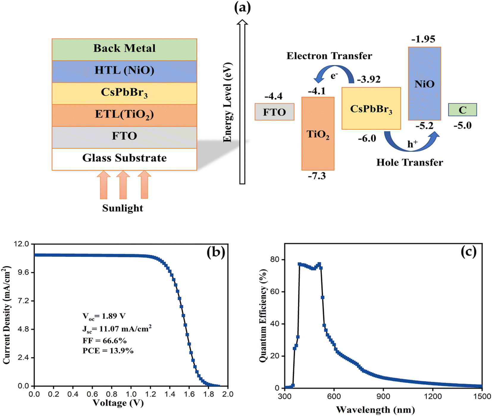 | ||
| Fig. 10 (a) Schematic illustration of proposed solar structure and its band energy alignment (b) J–V characteristic curves (c) quantum efficiency (Q.E) of simulated SC. | ||
| Parameters | FTO40 | TiO2 (ref. 40) | CsPbBr3 (ref. 40) | NiOx |
|---|---|---|---|---|
| W (nm) | 200 | 100 | 300 | 50 |
| Eg (eV) | 3.5 | 3.2 | 2.3 | 3.25 (exp.) |
| χ (eV) | 4 | 4 | 3.6 | 1.8 (ref. 40) |
| εr | 9 | 9 | 6.5 | 11.75 (ref. 40) |
| NC (cm−3) | 2.2 × 10¹⁷ | 2.2 × 10¹⁸ | 4.94 × 10¹⁷ | 2 × 10¹⁸ (ref. 40) |
| NV (cm−3) | 2.2 × 10¹⁶ | 1.8 × 10¹⁹ | 8.47 × 10¹⁸ | 2 × 10¹⁸ (ref. 40) |
| Vth e− (cm s−1) | 1 × 10⁷ | 1 × 10⁷ | 1 × 10⁷ | 1 × 10⁷ |
| Vth p (cm s−1) | 1 × 10⁷ | 1 × 10⁷ | 1 × 10⁷ | 1 × 10⁷ |
| μe (cm2 V−1 s−1) | 2 × 101 | 2 × 101 | 4.5 × 10³ | 8 |
| μp (cm2 V−1 s−1) | 1 × 101 | 1 × 101 | 4.5 × 10³ | 2 (exp.) |
| NA (cm−3) | — | — | — | 6.8 × 10¹⁴ (exp.) |
| ND (cm−3) | 1 × 10²⁰ | 2 × 10¹⁹ | 1 × 10⁵ | —40 |
J–V characteristics and quantum efficiency (Q.E) curves have been depicted in Fig. 10b and c, respectively. From the J–V measurements we observed the PCE of 13.9% (Jsc of 11.07 mA cm−2, Voc of 1.89 V, FF of 66.6%) for proposed solar cell (SC). Quantum efficiency (Q.E) for simulated solar cell showing a high quantum efficiency at visible region ranging from 390 nm to 530 nm, which is indicated to a considerable optical characteristics of proposed SC.
Literature study indicated that, Ruxin Guo et al. reported an efficiency of 11.21% by introducing an ionic liquid (DTPT) into CsPbBr3-based solar cell (SC) and that is the maximum PCE value ever recorded experimentally for CsPbBr3-based SC.41
In 2018, Haiwen Yuan et al. implanted NiOx as hole transporting material in CsPbBr3-based SC and obtained a PCE of 7.29%.42 Most recently, Yu Zou et al. also fabricated a CsPbBr3-photovoltaic device with incorporating NiOx nano-crystal thin film and enhanced the efficiency at around 9.19%.43 In order to investigate the potential of NiOx as a HTL layer in CsPbBr3-based SC, a numerical simulation was carried out to elucidate the combinatorial effects of carrier concentration and hole mobility of NiOx thin film on the overall photovoltaic performance parameters of CsPbBr3 device.
Fig. 11, illustrates the performance parameters of simulated CsPbBr3 solar cell with different carrier concentration and hole mobility of NiOx HTL layer. To investigate the influence of HTL carrier concentration (p) and hole mobility (μp) on device performances, p and μp were varied from 1 × 1013 cm−3 to 1 × 1019 cm−3 and 0.001 cm2 V−1 s−1 to 100 cm2 V−1 s−1, respectively. According to Fig. 11, the maximum values of p (1 × 1019 cm−3) and μp (100 cm2 V−1 s−1) provide the highest PCE value at around 15.44% for simulated device. The reason of the increment in PCE value is due to fact that, when p rises HTL's internal electric field also rises, causing an increase in charge conductivity and transport velocity.44 On the other hand, an increment in hole mobility (μp) will increase the diffusion length of charge carriers, that will make it easier to transport charge carriers without large amount of recombination and subsequently resulting higher PCE value.45 Table 4 below shows the carrier concentration and hole mobility of NiOx thin film from the various previous works, as well as the values obtained from this study.
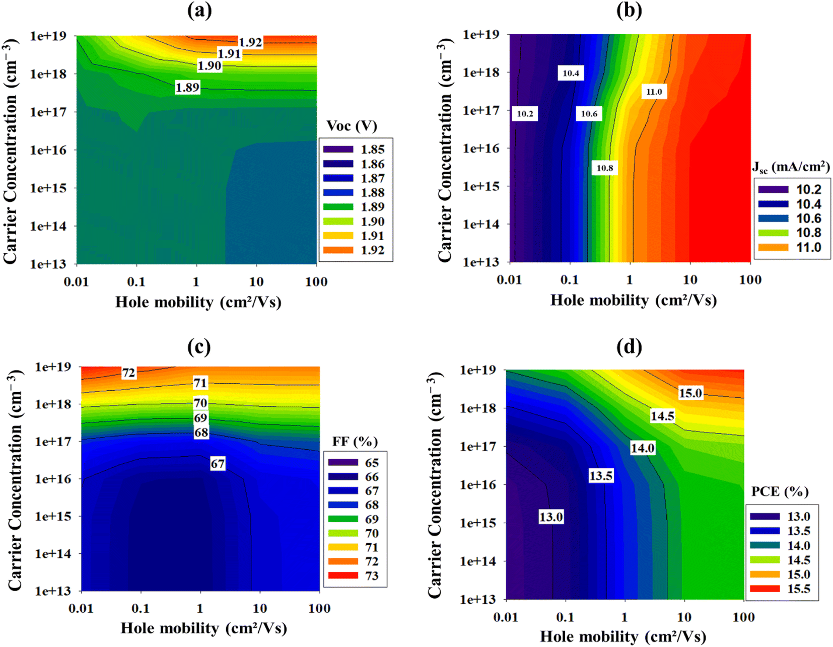 | ||
| Fig. 11 (a) Performance parameters of CsPbBr3 solar cell with different carrier concentration (p) and hole mobility (μp) of NiOx HTL layer (a) μp vs. p vs. Voc (b) μp vs. p vs. Jsc (c) μp vs. p vs. FF (%) (d) μp vs. p vs. PCE (%). | ||
| NiOx thin film | Carrier concentration (cm−3) | Hole mobility (cm2 V−1 s−1) | References |
|---|---|---|---|
| Boric acid mediated (BA)-NiOx | 2.17 × 10¹⁹ | 5.35 × 10⁻² | 46 |
| NiOx | 4.08 × 10¹⁸ | 2.41 × 10⁻² | 46 |
| Fe-NiOx | 3.331 × 10¹² | 6.22 | 47 |
| NiOx | 1.93 × 10¹² | 2.60 | 47 |
| Cu-NiOx | 2.16 × 10¹⁶ | 40 × 10−2 | 48 |
| NiOx | 1.50 × 10¹⁶ | 14 × 10−2 | 48 |
| NiOx | 1.37 × 10¹⁷ | 1.32 × 10⁻³ | 49 |
| TPA-derived NiOx | 6.8 × 10¹⁴ | 2 | This work |
By comparing the results from Fig. 11 and Table 4, it is evident that, there exist a large room for improvement in both carrier concentration and hole mobility parameters of NiOx thin film that needs to be implemented, if the current record efficiency of CsPbBr3 solar cell is to be surpassed.
4 Conclusions
In this work, MOF derived NiOx nanoparticles were synthesized by utilizing four distinct ligands (BTC/TPA/ATPA/DHTPA). A comparative investigation on the structural, morphological and optical properties of the MOF-derived synthesized NPs have been carried out. The findings of the FeSEM analysis demonstrate that the synthesized NiOx NPs have variable morphological structure, depending on the ligand of MOFs as well as with the calcination temperature. From the FeSEM, it was observed that, the TPA-derived NiOx exhibited relatively a small particle size (25–50 nm) with homogenous distribution compare to others, where ATPA derived NiOx NPs showed the most significant morphological changes. The fabrication of NiOx-thin film was also carried out by employing TPA-derived NiOx (600 °C). The structural, optical and electrical characteristics of the thin film have also been studied, where thin film showing a cubic phase structure with the band gap of 3.25 eV. Carrier concentration, hole mobility and resistivity were measured to be 6.8 × 1014 cm−3; 4.7 × 10¹⁴ Ω cm and 2.0 cm2 V−1 s−1, respectively. A numerical simulation was also performed to investigate the photovoltaic performance of the TPA-derived NiOx thin film. The efficiency of the device was measured at around 13.9% with the Jsc of 11.07 mA cm−2, Voc of 1.89 V and FF of 66.6%.Conflicts of interest
There are no conflicts to declare.Acknowledgements
We appreciate the Universiti Kebangsaan Malaysia (UKM) (@The National University of Malaysia) for the financial assistance through the SRF – APP MIMOS UKM grant (RS-2021-003). The authors extend their appreciation to Researchers Supporting Project number (RSP2023R34), King Saud University, Riyadh, Saudi Arabia. The authors also gratefully acknowledge Dr Marc Burgelman, University of Gent, Belgium, for providing the SCAPS- 1D simulation software.References
- Y. Wu, Y. He, T. Wu, T. Chen, W.-z. Weng and H.-L. Wan, Mater. Lett., 2007, 61, 3174–3178 CrossRef CAS.
- K. Anandan and V. Rajendran, Mater. Sci. Semicond. Process., 2011, 14, 43–47 CrossRef CAS.
- M.-S. Wu and Y.-P. Lin, Electrochim. Acta, 2011, 56, 2068–2073 CrossRef CAS.
- Y. Wang, J. Zhu, X. Yang, L. Lu and X. Wang, Thermochim. Acta, 2005, 437, 106–109 CrossRef CAS.
- Y.-Z. Zheng and M.-L. Zhang, Mater. Lett., 2007, 61, 3967–3969 CrossRef CAS.
- A. Aslani, V. Oroojpour and M. Fallahi, Appl. Surf. Sci., 2011, 257, 4056–4061 CrossRef CAS.
- A. C. Johnston-Peck, J. Wang and J. B. Tracy, ACS Nano, 2009, 3, 1077–1084 CrossRef CAS PubMed.
- J. Bandara, C. M. Divarathne and S. D. Nanayakkara, Sol. Energy Mater. Sol. Cells, 2004, 81, 429–437 CrossRef CAS.
- R. Kaneko, H. Kanda, K. Sugawa, J. Otsuki, A. Islam and M. K. Nazeeruddin, Sol. RRL, 2019, 3, 1900172 CrossRef.
- X. Wang, J. Song, L. Gao, J. Jin, H. Zheng and Z. Zhang, Nanotechnology, 2005, 16, 37 CrossRef CAS.
- P. Justin, S. K. Meher and G. R. Rao, J. Phys. Chem. C, 2010, 114, 5203–5210 CrossRef CAS.
- Y.-H. Seo, I. H. Cho and S.-I. Na, J. Alloys Compd., 2019, 797, 1018–1024 CrossRef CAS.
- P.-H. Lee, T.-T. Wu, C.-F. Li, D. Głowienka, Y.-H. Sun, Y.-T. Lin, H.-W. Yen, C.-G. Huang, Y. Galagan, Y.-C. Huang and W.-F. Su, Chem. Eng. J., 2021, 412, 128746 CrossRef CAS.
- S. Wang, Y. Li, J. Yang, T. Wang, B. Yang, Q. Cao, X. Pu, L. Etgar, J. Han, J. Zhao, X. Li and A. Hagfeldt, Angew. Chem., Int. Ed., 2022, 61, e202116534 CAS.
- S. Pilban Jahromi, N. M. Huang, M. R. Muhamad and H. N. Lim, Ceram. Int., 2013, 39, 3909–3914 CrossRef CAS.
- G. Thangamani J., K. Deshmukh, B. Ahamed, K. Chidambaram, K. Saranya and S. Pasha, Int. J. ChemTech Res., 2015, 8, 974–4290 Search PubMed.
- Y. Sun and H.-C. Zhou, Sci. Technol. Adv. Mater., 2015, 16, 054202 CrossRef PubMed.
- D. Y. Heo, H. H. Do, S. H. Ahn and S. Y. Kim, Polymers, 2020, 12, 2061 CrossRef CAS PubMed.
- L. Pan, T. Muhammad, L. Ma, Z.-F. Huang, S. Wang, L. Wang, J.-J. Zou and X. Zhang, Appl. Catal., B, 2016, 189, 181–191 CrossRef CAS.
- T. Prabhakaran, R. V. Mangalaraja, J. C. Denardin and J. A. Jiménez, J. Alloys Compd., 2017, 716, 171–183 CrossRef CAS.
- N. C. Horti, M. D. Kamatagi, S. K. Nataraj, M. N. Wari and S. R. Inamdar, Nano Express, 2020, 1, 010022 CrossRef.
- S. Suresh and J. Podder, Int. J. Nanopart., 2015, 8, 289–301 CrossRef.
- Q. Hongxia, W. Zhiqiang, Y. Hua, Z. Lin and Y. Xiaoyan, J. Nanomater., 2009, 479 Search PubMed.
- V. Selvanathan, M. Shahinuzzaman, S. Selvanathan, D. K. Sarkar, N. Algethami, H. I. Alkhammash, F. H. Anuar, Z. Zainuddin, M. Aminuzzaman, H. Abdullah and M. Akhtaruzzaman, Catalysts, 2021, 11, 1523 CrossRef CAS.
- N. Saikumari, S. M. Dev and S. A. Dev, Sci. Rep., 2021, 11, 1734 CrossRef CAS PubMed.
- T. Sinha, L. Verma and A. Khare, Appl. Phys. A: Mater. Sci. Process., 2020, 126, 867 CrossRef CAS.
- W. W. Lestari, I. D. Winarni and F. Rahmawati, IOP Conf. Ser.: Mater. Sci. Eng., 2017, 172, 012064 Search PubMed.
- F. Wang, X. Chen, L. Chen, J. Yang and Q. Wang, Mater. Sci. Eng., C, 2019, 96, 41–50 CrossRef CAS PubMed.
- R. Salama, S. Abd El-Hakam, S. Samra, S. El-dafrawy and A. Ahmed, Int. J. Mod. Chem., 2018, 20(10), 195–207 Search PubMed.
- S. Yang, J. Zhang, C. Bai and K. Deng, Can. J. Chem., 2020, 99, 465–473 CrossRef.
- Y. Liao, C. Li, X. Lou, P. Wang, Q. Yang, M. Shen and B. Hu, J. Colloid Interface Sci., 2017, 506, 365–372 CrossRef CAS PubMed.
- J.-J. Song, B. He, X. Wang, Y. Guo, C. Peng, Y. Wang, Z. Su and Q. Hao, J. Mater. Sci., 2021, 56, 17178–17190 CrossRef CAS.
- S. D. Khairnar and V. S. Shrivastava, J. Taibah Univ. Sci., 2019, 13, 1108–1118 CrossRef.
- S. Pilban Jahromi, A. Pandikumar, B. T. Goh, Y. S. Lim, W. J. Basirun, H. N. Lim and N. M. Huang, RSC Adv., 2015, 5, 14010–14019 RSC.
- Z. Sabouri, N. Fereydouni, A. Akbari, H. A. Hosseini, A. Hashemzadeh, M. S. Amiri, R. Kazemi Oskuee and M. Darroudi, Rare Met., 2020, 39, 1134–1144 CrossRef CAS.
- A. Barakat, M. Al-Noaimi, M. Suleiman, A. S. Aldwayyan, B. Hammouti, T. B. Hadda, S. F. Haddad, A. Boshaala and I. Warad, Int. J. Mol. Sci., 2013, 14, 23941–23954 CrossRef PubMed.
- S.-J. Hong, H.-J. Mun, B.-J. Kim and Y.-S. Kim, Micromachines, 2021, 12, 1168 CrossRef PubMed.
- Z.-W. Huang, S.-H. Yang, Z.-Y. Wu and H.-C. Hsu, ACS Omega, 2021, 6, 15855–15866 CrossRef CAS PubMed.
- S. Jana, G. Mondal, B. C. Mitra, P. Bera, B. Chakraborty, A. Mondal and A. Ghosh, New J. Chem., 2017, 41, 14985–14994 RSC.
- S. Rani, D. Kuar, V. Jeyachandran and D. S. Ghosh, Opt. Mater., 2022, 131, 112612 CrossRef CAS.
- R. Guo, J. Xia, H. Gu, X. Chu, Y. Zhao, X. Meng, Z. Wu, J. Li, Y. Duan, Z. Li, Z. Wen, S. Chen, Y. Cai, C. Liang, Y. Shen, G. Xing, W. Zhang and G. Shao, J. Mater. Chem. A, 2023, 11, 408–418 RSC.
- H. Yuan, Y. Zhao, J. Duan, Y. Wang, X. Yang and Q. Tang, J. Mater. Chem. A, 2018, 6, 24324–24329 RSC.
- Y. Zou, F. Cao, P. Chen, R. He, A. Tong, C. Yin, Z. Lan, W. Sun and J. Wu, Electrochim. Acta, 2022, 435, 141392 CrossRef CAS.
- G. Pindolia, S. M. Shinde and P. K. Jha, Sol. Energy, 2022, 236, 802–821 CrossRef CAS.
- C. Pinzón, N. Martínez, G. Casas, F. C. Alvira, N. Denon, G. Brusasco, H. Medina Chanduví, A. V. Gil Rebaza and M. A. Cappelletti, Solar, 2022, 2, 559–571 CrossRef.
- B. Ge, Z. Q. Lin, Z. R. Zhou, H. W. Qiao, A. P. Chen, Y. Hou, S. Yang and H. G. Yang, Sol. RRL, 2021, 5, 2000810 CrossRef CAS.
- P. S. Chandrasekhar, Y.-H. Seo, Y.-J. Noh and S.-I. Na, Appl. Surf. Sci., 2019, 481, 588–596 CrossRef CAS.
- M. Feng, M. Wang, H. Zhou, W. Li, S. Wang, Z. Zang and S. Chen, ACS Appl. Mater. Interfaces, 2020, 12, 50684–50691 CrossRef CAS PubMed.
- X. Jin, Y. Yuan, C. Jiang, H. Ju, G. Jiang, W. Liu, C. Zhu and T. Chen, Sol. Energy Mater. Sol. Cells, 2018, 185, 542–548 CrossRef CAS.
| This journal is © The Royal Society of Chemistry 2023 |