
 Open Access Article
 This Open Access Article is licensed under a Creative Commons Attribution-Non Commercial 3.0 Unported Licence
Sputtered anti-reflection layer on transparent polyimide substrate improves adhesion strength to copper layer: effects of layer thickness and sputtering power
Yuan-Nan Tsaiab,
Shih-Chieh Chinc,
Hsin-Yo Chenc,
Ta-I. Yang d,
Mei-Hui Tsai*bc and
I.-Hsiang Tseng*e
d,
Mei-Hui Tsai*bc and
I.-Hsiang Tseng*e
aDepartment of Electronic Engineering, Lunghwa University of Science and Technology, Guishan, Taoyuan 333326, Taiwan
bGraduate Institute of Precision Manufacturing, National Chin-Yi University of Technology, Taichung, 411030, Taiwan. E-mail: tsaimh@ncut.edu.tw
cDepartment of Chemical and Materials Engineering, National Chin-Yi University of Technology, Taichung, 411030, Taiwan. E-mail: tsaimh@ncut.edu.tw
dDepartment of Chemical Engineering, Chung-Yuan Christian University, Chungli, Taoyuan 320314, Taiwan
eDepartment of Chemical Engineering, Feng Chia University, Taichung, 407102, Taiwan. E-mail: ihtseng@fcu.edu.tw
First published on 5th May 2023
Abstract
In order to shield the electronic circuits on a transparent polyimide (PI) substrate, an anti-reflection (AR) layer was deposited on a PI film via DC reactive magnetron sputtering. The effects of sputtering power and thickness of AR layer on the optical property and adhesion strength of the PI were investigated. The composition of the AR layer influences the bonding between layers. Sufficient thickness of the AR layer is essential to strengthen the adhesion between the PI and copper (Cu) layers. The sputtered AR layer on the PI also improves the barrier property for water vapor. The AR layer-sputtered PI substrates remain transparent and exhibit high peel strength to the Cu layer, suggesting their potential applications as reliable transparent substrates for modern electronic devices.
Introduction
Displays have become a necessity for human beings as they appear in everyday items such as smartphones, tablet devices, car monitors and wearable devices. Among them, the combination of wearable devices and the Internet of Things will enable an efficient and easy life for future smart living. For wearable devices, soft transparent panels with conductive circuits are indispensable materials. The materials for transparent panel must be bendable, transparent, ultra-thin, and sufficiently stiff for the substrate.1–4 Colorless polyimide (PI) has been regarded as the preferred material for flexible transparent panels because of its high optical transmittance, high thermal stability, low dielectric constant, and excellent resistance to chemical solvents.3–7 However, the circuit patterns deposited on colorless PI substrates would be visible to the naked eye. Therefore, an anti-reflective (AR) layer is often fabricated between colorless PI and electronic circuits to hide the electronic circuits.1,8–10From our previous work, the deposition of AR layers on colorless PI substrates successfully enhances the adhesion strength between PI and the copper (Cu) layer, which mimics the electronic circuits.8 By adjusting the parameters, such as gas composition, of DC reactive magnetron sputtering, the AR layer-coated transparent PI substrates not only exhibit high adhesion strength to the Cu layer but low reflectance, indicating its potential as advanced flexible printed circuit material. In this work, we further investigate the effects of the AR-layer thickness and the sputtering power on the adhesive and optical properties of PI composite films. An optimum thickness of the AR layer, which contains copper and nickel oxides, is critical for the following deposition of conductive copper layer with sufficient adhesion to the PI substrate. The correlation of the bonding at the interface to the peeling strength of the PI substrate was also investigated. The AR-layer deposited transparent electronic substrates show the potential for future applications in soft panel displays and wearable devices.
Experimental
Materials and sample preparation
According to our previous work, the presence of primer layer on fluorinated PI significantly improves the adhesion strength.8 Therefore, the transparent PI films (thickness = 25 ± 1 μm) coated with a thin layer of primer (thickness = 1.1 ± 0.1 μm) provided by Pomiran Metalization Research Co., Ltd. were selected as the substrates in this work.A PI strip with a fixed dimension of 6 cm by 9 cm was taped to a glass substrate, and then purged with air to clean the surface. As illustrated in Scheme 1, a DC-reactive magnetron sputtering machine (KAO-DUEN, SPLTTER) equipped with a Cu–Ni alloy target (Cu/Ni = 75/25 wt% and purity = 99.95%) was used to deposit Cu–Ni oxides as the AR layer on transparent PI. The working pressure of the sputtering chamber was fixed at 6 × 10⁻³ torr, and the substrate temperature was 50 °C. The gas flowrate was 27 sccm for Ar and 3 sccm for O2. The thickness of the AR layer deposited on PI was 100 ± 25 Å, 300 ± 40 Å, or 500 ± 50 Å, respectively, under the sputtering power of 300 W (83.93 W/in2). For the AR layer with the thickness of 500 Å, the sputtering power was further changed, ranging from 225 W (62.95 W/in2) to 450 W (125.90 W/in2). On the top of each AR layer, the conductive Cu layer with a thickness of 1000 Å was then deposited. The sample name was denoted as S-PI-x-y, where x represents the thickness of AR layer (x = 100, 300, or 500 Å) and y represents the sputtering power (y = 225, 300, 450 W), respectively.
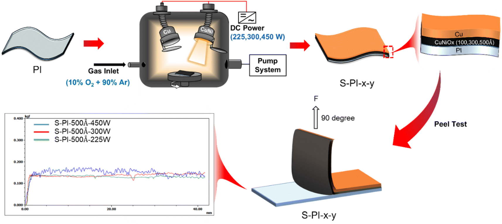 | ||
| Scheme 1 The deposition of AR layer and Cu layer on PI substrates, followed by the peel test. | ||
Characterization of samples
The thickness of AR layer or copper layer was determined by a surface profiler (α-step). The UV-vis spectrophotometer (JASCO V-750) was used to measure the reflectance and transmission of film samples. The surface morphology of the film was observed via a white light interference (WLI) microscope (ZYGO, NEWVIEW 8300). A peeling tester provided by Taimide Tech. Inc. was applied to measure the adhesion (peel) strength following the test method of IPC-TM-650 2.4.9 with a tensile force of 5 kg and a tensile rate of 0.85 mm s−1. The elemental composition and bonding on the peeled surface were detected by the energy-dispersive X-ray spectroscopy (EDS, JEOL JSM-7401) and the X-ray photoelectron spectroscopy (XPS, ULVAC PHI-5000). A haze meter (NIPPON DENSHOKU NDH-2000N) was used to measure the haze of each film. The water permeability of samples at 760 mmHg and 40 °C was evaluated by a water permeability tester (MOCON PERMATRAN – W Model 3/61).Results and discussion
Location of the delaminated layers
The peel test was conducted to evaluate the effect of deposited layers on the adhesion strength of PI substrate to Cu layer. Fig. 1 displays the photos of the delaminated two sides after peeling tests. As shown in Fig. 1, two types of delaminated layers appear from the S-PI-x-300 W samples. When the thickness of AR layer is 100 Å, many residuals of the black AR layer are visible from the colorless PI side (Fig. 1(a)). At the same time, the Cu layer on the other side reveals the color of copper (Fig. 1(a′)). Therefore, the peeling occurs at the interface between AR and Cu layers. On the other hand, when the thickness of AR layer is 300 Å or 500 Å, most of the black AR layer is observed from the Cu side rather than the PI side. That is, the delamination of S-PI-300 Å-300 W and S-PI-500 Å-300 W occurs at the interface of PI and AR layers, if the AR layer is thicker.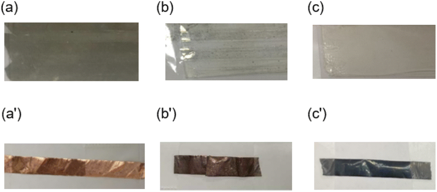 | ||
| Fig. 1 Photos of (a–c) colorless PI side and (a′–c′) metal (Cu) side of delaminated S-PI-x-300 W after peel test. The thickness (x) of the AR layer on PI is (a, a′) 100 Å, (b, b′) 300 Å, and (c, c′) 500 Å. | ||
The elemental composition of the delaminated surface of the PI side was further determined by EDS. As shown in Fig. 2, the ratio of Cu and Ni significantly decreases with the increasing thickness of AR layer. Notably, copper and nickel oxides are the components of AR layer, and consequently the results further confirm the location of the peeling surface. When the thickness of AR layer increases to 300 Å, the delamination occurs at the interface of AR and PI that the residual Cu or Ni on PI dramatically decreases. At the same time, the content of F increases due to the exposure of fluorinated PI matrix.
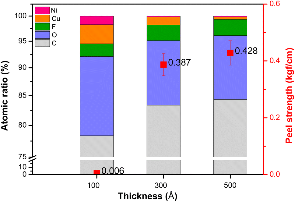 | ||
| Fig. 2 The peel strength and atomic ratio of Ni, Cu, F, O, and C from the PI side of S-PI-x-300 W after peel tests. The thickness (x) of the AR layer is 100, 300, and 500 Å, respectively. | ||
Effect of AR layer on adhesion strength and reflectance
The location of the delamination implied the adhesion strength of S-PI-x-300 W. As shown in Fig. 2, the peel strength of S-PI-x-300 W increases when the thickness of AR layer (x) increases or when the peeling occurs between the PI and AR layers. That is, the bonding between PI and Cu layers is successfully enhanced with the coating of AR layer with sufficient thickness. The reason for the enhanced adhesion strength can be explained by the following WLI results. The WLI image illustrated in Fig. 3 reveals the surface roughness of 11 nm for intrinsic PI substrate. When the thickness of the AR layer is only 100 Å, the deposited AR layer could not fully cover the surface of PI substrate. The interaction between PI matrix and Cu layer is weak so that a low peel strength of 0.006 kgf cm−1 is revealed and resulting in the delamination at the interface between the AR and Cu layers.3 On the other hand, delamination occurs at the interface of PI and AR layers when the thickness of AR layer reaches 300 Å. In this case, the AR layer strongly bonds with Cu layer that the peeling strength increases to over 0.3 kgf cm−1.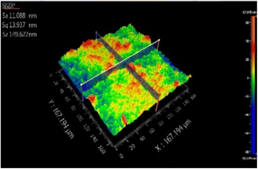 | ||
| Fig. 3 WLI image of PI substrate. | ||
As a reflectance of less than 15% is a requirement for fabricating the AR layer to effectively shield the conductive copper layers of electronic circuits on transparent PI, the reflectance from the PI surface was verified and measured as shown in the insets of Fig. 4. The reflectance of the PI composite films, which contain the PI substrate and coated AR and Cu layers, decreases with the increasing thickness of the AR layer under the same sputtering power of 300 W (Fig. 4(a)). Sputtering the AR layer with a thickness of 500 Å revealed the lowest reflectance, as well as the highest peel strength as shown in Fig. 2. When the thickness of AR layer is fixed to 500 Å, the films sputtering under the power of 450 W exhibits the lowest reflectance at 550 nm as shown in Fig. 4(b). Notably, when the sputtering power is 225 W, the reflectance is greater than 20% for S-PI-500 Å-225 W. In contrast, the reflectance in the visible light region (400 to 700 nm) is less than 10% for S-PI-500 Å-300 W.
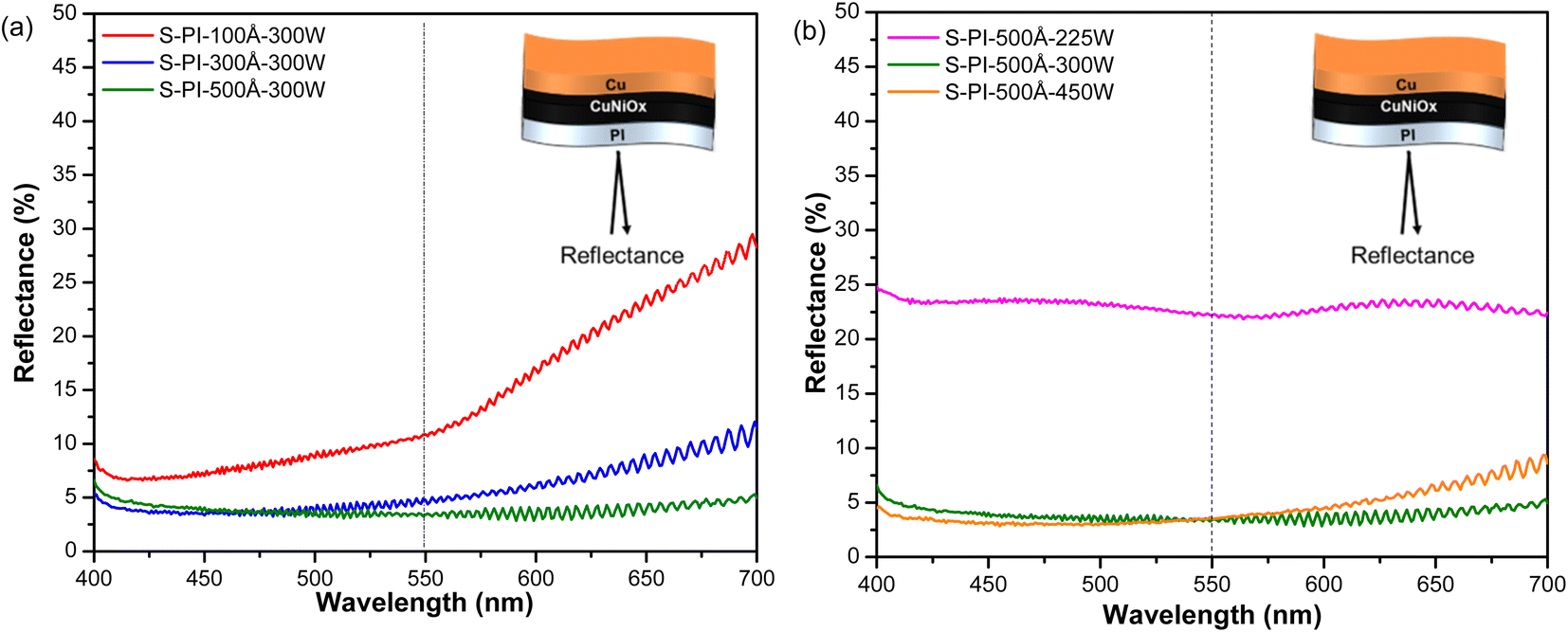 | ||
| Fig. 4 Reflectance from the PI surface of S-PI-x-y films. (a) x = 100, 300, 500 Å; y = 300 W. (b) x = 500 Å; y = 225, 300, 450 W. | ||
The results of the peel strength and reflectance of S-PI-500 Å-y films are summarized in Table 1. The peel strength of films increases with the sputtering power. As the sputtering power increases, more target particles eject from the sputter target, resulting in a higher deposition rate on the substrate. In addition, the high sputtering power also leads to the ejected target particles with high energy to break more bonds on the substrate.11,12 The high energy deposition process will improve the interaction between the substrates and the deposited films. According to the EDS results listed in Table 1, the oxygen contents from delaminated surface of the AR side slightly increase with the sputtering power. The high energy deposition process results in more oxygen in the film that made the film darker. Therefore, the improved absorption of incident light makes the film reflect less lights.13,14
| Sample | Peel strength (kgf cm−1) | Oxygen content of AR layer (%) | WVTR (g-mil/m2-day) | Transmittance @ 550 nm (%) | Haze (%) |
|---|---|---|---|---|---|
| PI | — | — | 242.9 ± 23.64 | 90.3 | 0.31 |
| S-PI-500 Å-225 W | 0.422 ± 0.006 | 10.90 | 4.023 ± 0.626 | 90.2 | 0.68 ± 0.07 |
| S-PI-500 Å-300 W | 0.428 ± 0.013 | 12.19 | 1.715 ± 0.826 | 90.1 | 0.70 ± 0.08 |
| S-PI-500 Å-450 W | 0.441 ± 0.019 | 12.33 | 1.505 ± 0.167 | 90.1 | 1.07 ± 0.30 |
The XPS spectra of the delaminated surface of PI side from S-PI-500 Å-y are compared to elucidate the relationship between the adhesion strength and the bonding at the interface. The XPS full scan spectra of films shown in Fig. 5(a) suggest the existence of C, N, and O signals, which are the elements of PI substrate, as well as the signals of Cu and Ni, which indicate the remaining elements from AR layer after peeling test. The XPS spectra of C 1s region shown in Fig. 5(b–d) are deconvoluted into the following binding energies of 284.7 eV, 285.6 eV, 286.3 eV, and 288.6 eV, which represent the C–C, C–N, C–O, and C![[double bond, length as m-dash]](https://www.rsc.org/images/entities/char_e001.gif) O bonding, respectively.15–18 The effects of the sputtering power on the bonding ratio on the peel strength was plotted in Fig. 6. The ratio of C–N bonding decreases with increasing sputtering power, while the content of C–O bonding increases. The high energy sputtering process leads to the breakage of C–N bonds and promotes the formation of C–O bonds.17–19 As Ni or Cu is easily bonded with C–O on PI, the interaction between AR layer and PI is strengthened to enhance the peel strength.3,7,19,20 Therefore, the increasing trend of peel strength is consistent with the increasing trend of C–O bonding ratio on PI.
O bonding, respectively.15–18 The effects of the sputtering power on the bonding ratio on the peel strength was plotted in Fig. 6. The ratio of C–N bonding decreases with increasing sputtering power, while the content of C–O bonding increases. The high energy sputtering process leads to the breakage of C–N bonds and promotes the formation of C–O bonds.17–19 As Ni or Cu is easily bonded with C–O on PI, the interaction between AR layer and PI is strengthened to enhance the peel strength.3,7,19,20 Therefore, the increasing trend of peel strength is consistent with the increasing trend of C–O bonding ratio on PI.
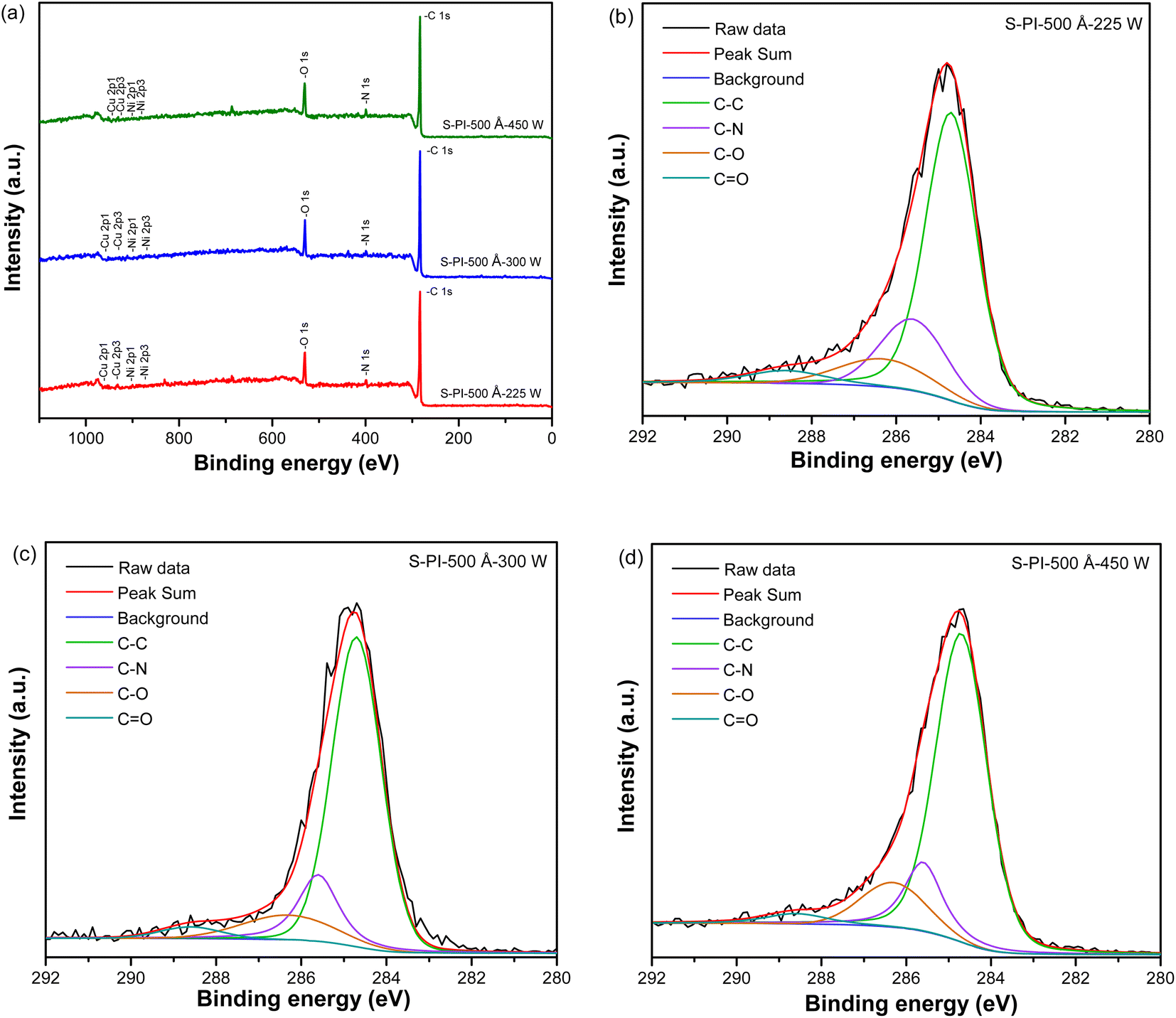 | ||
| Fig. 5 (a) XPS full scan spectra of S-PI-500 Å-y. Deconvoluted XPS C1s spectra of (b) S-PI-500 Å-225 W, (c) S-PI-500 Å-300 W and (d) S-PI-500 Å-450 W. | ||
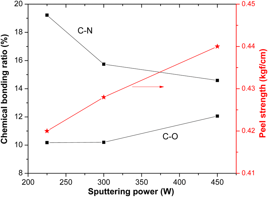 | ||
| Fig. 6 Effects of sputtering power (y) on the chemical bonding ratio and peel strength of S-PI-500 Å-y films. | ||
Optical and barrier properties of AR layer-coated PI
In order to investigate the effect of sputtering power on the optical property of PI substrates, the deposited AR layer was etched with hydrochloric acid to expose the PI substrate for the measurements of transmittance and haze values. The optical transmittance shown in Fig. 7 suggests that the AR-layer deposition process did not sacrifice the original high-transparency of the PI substrates. As listed in Table 1, the haze of the remaining PI substrate is 0.68%, 0.70% and 1.07% for the films sputtering at 225, 300, and 450 W, respectively, compared to the haze of 0.31% for original PI substrate. A higher haze value than the parent PI substrate indicates that more internal scattering occurred within the substrate.1,4 Therefore, an increase in haze indicates the damage to the PI structure under high energy deposition process. However, the highest haze value of 1.07% is still below the acceptable range (less than 1.1%) for commercial applications.1,4 The transparency of all PI substrates remains as high as 90% throughout the visible light range. The well-tuned sputtering conditions not only provide anti-reflective property to PI composites but maintain good optical properties to PI substrates.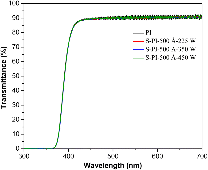 | ||
| Fig. 7 UV-vis spectra of original PI and remaining PI substrates after etching AR layer from S-PI-500 Å-y films. Etching the AR layer. | ||
The barrier property is another critical property for electronic materials. High water vapor transmission rate (WVTR) will reduce the adhesive strength or reliability of the film.5,21 The WVTR values of S-PI-500 Å-y films were also verified in this work, and the results were listed in Table 1. The WVTR of the original PI substrate is about 242.9 g-mil/m2-day. After sputtering with AR layer, a significant decrease in WVTR is revealed. For the same thickness of 500 Å, the deposition of AR layer at higher sputtering power exhibits better barrier property. The lowest WVTR value of 1.505 g-mil/m2-day is obtained from S-PI-500 Å-450 W. The high-energy deposition process provides more energy to the ejected target particles, making them easier to migrate on the PI substrate. Therefore, a denser AR layer structure is formed on PI, which effectively inhibits water penetration.12,22
Conclusions
In this work, we successfully tuned the depositing process to optimize the thickness, density, and composition of AR layers to obtain PI composite films with sufficient adhesion strength and optical properties. The thickness of AR layer needs to be greater than the roughness of original PI substrate to effectively increase the interaction with the following deposited Cu layer. The increase in the sputtering power leads to the increase in oxygen content of AR layer, the decrease in reflectivity of composite film, and the enhance in adhesion strength. In addition, the high-energy deposition process can increase the density of the film and consequently reduce the water penetration rate through the film. The results suggested that the optimized AR-layer sputtering process improves the reliability of the transparent PI-based composite film as a flexible, anti-reflective transparent printed circuit board material for practical applications.Conflicts of interest
There are no conflicts to declare.Acknowledgements
The authors would like to acknowledge Taimide Tech. Inc. and Pomiram Metalization Research for providing PI substrates and peel tests. The authors also appreciate the financial support from the National Science and Technology Council of Taiwan under the grant numbers of MOST 109-2622-E-167-021 and MOST 109-2221-E-035-019-MY3.References
- H. W. Yun, G. M. Choi, H. K. Woo, S. J. Oh and S. H. Hong, Curr. Appl. Phys., 2020, 20, 1163–1170 CrossRef.
- X. Z. Huang, F. H. Zhang, Y. J. Liu and J. S. Leng, ACS Appl. Mater. Interfaces, 2020, 12, 23236–23243 CrossRef CAS PubMed.
- J. J. Chen, Q. An, R. D. Rodriguez, E. Sheremet, Y. Wang, E. Sowade, R. R. Baumann and Z. S. Feng, Appl. Surf. Sci., 2019, 487, 503–509 CrossRef CAS.
- J. L. Shen, F. Li, Z. H. Cao, D. Barat and G. L. Tu, ACS Appl. Mater. Interfaces, 2017, 9, 14990–14997 CrossRef CAS PubMed.
- Y. W. Liu, A. Tang, J. H. Tan, Y. H. Li, D. Wu, X. Zhang, X. Q. Zhao, P. He and H. L. Zhang, React. Funct. Polym., 2020, 157, 104747 CrossRef CAS.
- Y. J. Choi, J. H. Ko, S. W. Jin, H. S. An, D. B. Kim, K. H. Yoon, H. W. Kim and C. M. Chung, Polymers, 2021, 13(23), 4100 CrossRef CAS PubMed.
- B. I. Noh, J. W. Yoon and S. B. Jung, Microelectron. Eng., 2011, 88, 1024–1027 CrossRef CAS.
- Y. N. Tsai, S. C. Chin, H. Y. Chen, M. S. Li, Y. S. Chen, Y. L. Wang, M. H. Tsai and I. H. Tseng, ACS Omega, 2023, 8(6), 5752–5759 CrossRef CAS PubMed.
- T. Okabe, T. Yano, K. Yatagawa and J. Taniguchi, Microelectron. Eng., 2021, 242, 111559 CrossRef.
- J. A. Lee, C. R. Lin, P. C. Pan, C. W. Liu and A. Y. T. Sun, Chem. Phys., 2020, 529, 110551 CrossRef CAS.
- H. Kakati, A. R. Pal, H. Bailung and J. Chutia, Appl. Surf. Sci., 2009, 255, 7403–7407 CrossRef CAS.
- M. H. Tsai, C. J. Chang, H. H. Lu, Y. F. Liao and I. H. Tseng, Thin Solid Films, 2013, 544, 324–330 CrossRef CAS.
- A. Parretta, M. K. Jayaraj, A. DiNocera, S. Loreti, L. Quercia and A. Agati, Phys. Status Solidi A, 1996, 155, 399–404 CrossRef CAS.
- K. Sahu, A. Bisht, S. A. Khan, I. Sulania, R. Singhal, A. Pandey and S. Mohapatra, Ceram. Int., 2020, 46, 14902–14912 CrossRef CAS.
- W. J. Lee, Y. S. Lee, S. K. Rha, Y. J. Lee, K. Y. Lim, Y. D. Chung and C. N. Whang, Appl. Surf. Sci., 2003, 205, 128–136 CrossRef CAS.
- Y. Li, Y. X. Wang, Y. Wang and Y. T. Wu, ACS Appl. Mater. Interfaces, 2023, 15(9), 12590–12602 CrossRef CAS PubMed.
- D. D. Ju, C. Y. Sun, H. Wang, X. M. Wang, Y. Y. Wu, Z. X. Dong and X. P. Qiu, RSC Adv., 2020, 10, 39572–39579 RSC.
- M. J. Chuang, Surf. Coat. Technol., 2009, 203, 3527–3532 CrossRef CAS.
- Y. J. Kim, S. B. Jin, S. I. Kim and J. G. Han, J. Adhes. Sci. Technol., 2011, 25, 993–1000 CrossRef CAS.
- S. B. Koo, C. M. Lee, S. J. Kwon, J. M. Jeon, J. Y. Hur and H. K. Lee, Met. Mater.-Int., 2019, 25, 117–126 CrossRef CAS.
- H. J. Lee and J. Yu, J. Electron. Mater., 2008, 37, 1102–1110 CrossRef CAS.
- M. C. Lin, C. H. Tseng, L. S. Chang and D. S. Wuu, Thin Solid Films, 2007, 515, 4596–4602 CrossRef CAS.
| This journal is © The Royal Society of Chemistry 2023 |