
 Open Access Article
 This Open Access Article is licensed under a Creative Commons Attribution-Non Commercial 3.0 Unported Licence
Highly C-oriented (002) plane ZnO nanowires synthesis
Ben Moussa Nizar ab,
Mohamed Lajnefb,
Julien Chastea,
Radouane Chtouroub and
Etienne Herth*a
ab,
Mohamed Lajnefb,
Julien Chastea,
Radouane Chtouroub and
Etienne Herth*a
aCentre de Nanosciences et de Nanotechnologies, CNRS UMR 9001, Univ. Paris-Sud, Université Paris-Saclay, Palaiseau 91120, France. E-mail: etienne.herth@c2n.upsaclay.fr
bLaboratory of Nanomaterials and Renewable Energy Systems, LANSER, Research and Technology Center of Energy, Borj-Cedria Science and Technology Park, BP 95, Hammam-Lif, 2050, Tunisia
First published on 16th May 2023
Abstract
Nanowires are widely used for energy harvesting, sensors, and solar cells. We report a study on the role of buffer layer in the growth of zinc oxide (ZnO) nanowires (NWs) synthesised by a chemical bath deposition (CBD) method. To control the thickness of the buffer layer, multilayer coatings corresponding to one layer (100 nm thick), three layers (300 nm thick), and six layers (600 nm thick) of ZnO sol–gel thin-films were used. The evolution of the morphology and structure of ZnO NWs was characterized by scanning electron microscopy, X-ray diffraction, photoluminescence, and Raman spectroscopy. Highly C-oriented ZnO (002)-oriented NWs were obtained on both substrates, silicon and ITO, when the thickness of the buffer layer was increased. The role of ZnO sol–gel thin films used as a buffer layer for the growth of ZnO NWs with (002)-oriented grains also resulted in a significant change in surface morphology on both substrates. The successful deposition of ZnO NWs on a variety of substrates, as well as the promising results, open up a wide range of applications.
1 Introduction
Piezoelectric and biocompatible materials, including zinc oxide (ZnO) and aluminium nitride (AlN), have found a wide range of applications.1–3 For these latter, the crystalline orientation of the c-axis, with preferential (002) planes, is required for piezoelectricity.4–6 Among them, ZnO is a unique material with excellent piezoelectric, optical and semiconductor properties. Recently, there has been a surge of interest in the fabrication and characterization of ZnO nanostructures such as ZnO nanowires (NWs).7 It has been found that ZnO nanowires can be used as a sensitive layer for sensing applications based on surface acoustic wave (SAW) devices and other detectors.8,9 ZnO NWs are gaining more and more attention from researchers around to the development of low-cost technology for solar energy harvesting in order to meet future energy needs without causing environmental harm.10,11 In addition, Zhong Lin Wang has demonstrated energy harvesters based on vertical ZnO nanowires.12 These organized structures based on ZnO NWs offer several applicative advantages due to their morphologies and dimensions in the piezoelectric field.13,14Several low-cost deposition techniques have been investigated, and it has been found that many important parameters, such as precursor concentration, growth temperature, buffer layer type and thickness, affect the formation of ZnO.15–17 The chemical bath deposition (CBD) technique has attracted the interest of the research community due to its simplicity, cost efficiency, low temperature and environmentally friendly growth deposition, as well as its ability to scale up to large areas for commercial production.18,19 However, the relationships between the buffer layer and C-oriented NWs properties with preferential (002) planes are rather few addressed in the literature.
Within this frame, the aim of our work was to optimize the growth process, both on Si and indium tin oxide (ITO) substrates, to obtain the proper ZnO NWs orientation in combination with a ZnO sol–gel thin-films as buffer layer. Further, we clarify the significance of different thicknesses of buffer layers on the growth of ZnO NWs by CBD. The emphasis is focus on the relationship between morphology, structure and optical properties.
2 Experimental
2.1 Synthesis of the buffer layer
The ZnO buffer layers were deposited using a sol–gel method detailed in our previous paper.20 Herein, the depositions of ZnO sol–gel buffer layer on Si 〈100〉 and glass ITO samples (1 cm × 1 cm) were carried out by spin coating method as presented in Fig. 1A and C. Briefly, the precursor ethanolamine (NH2CH2CH2OH) were used with ethanol (C2H6O) as stabilizer and solvent, respectively, and zinc acetate dihydrate (Zn[CH3COO]2·2H2O). The zinc acetate concentration was fixed at 0.75 M, while the molar ratio of zinc acetate dihydrate to ethanolamine was kept at 1![[thin space (1/6-em)]](https://www.rsc.org/images/entities/char_2009.gif) :1. In order to study the effect of the number of buffer layer, 1, 3 and 6 layers were deposited with spin coating technique. After deposition, these were dried at different temperatures from 100 to 300 °C for 20 min to evaporate the solvents and remove organic residues. Finally, the buffer layer with different thicknesses were annealed in air at 400 °C for 1 h.
:1. In order to study the effect of the number of buffer layer, 1, 3 and 6 layers were deposited with spin coating technique. After deposition, these were dried at different temperatures from 100 to 300 °C for 20 min to evaporate the solvents and remove organic residues. Finally, the buffer layer with different thicknesses were annealed in air at 400 °C for 1 h.
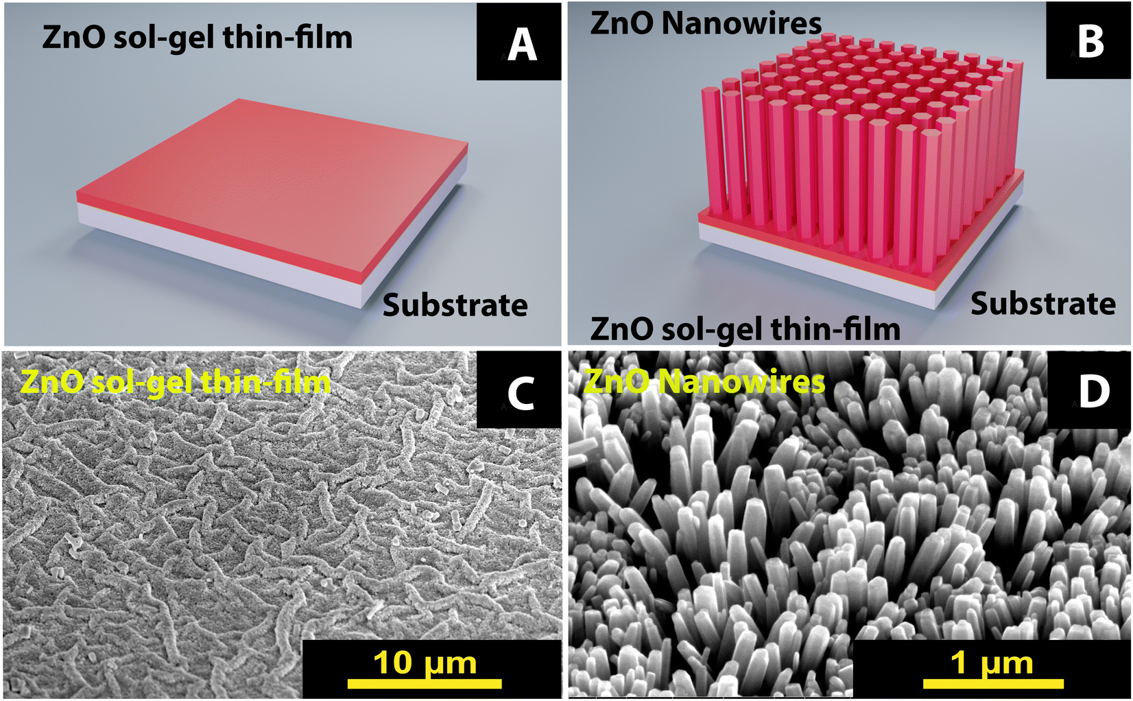 | ||
| Fig. 1 Schematic representation of the steps fabrication based on a combination of sol–gel synthesis and chemical bath deposition process of ZnO nanowires (A) on ZnO sol–gel thin-film deposited on substrate by spin coating, (B) ZnO nanowires arrays. (C) and (D), SEM images of the as-grown ZnO nanowire arrays on the substrate (C), ZnO sol–gel thin-film after spin-coating, and (D) ZnO nanowires grown. | ||
2.2 Synthesis of the nanowires
After the buffer layer preparations, ZnO nanowires (NWs) are prepared by the chemical bath deposition (CBD) method as shown in Fig. 1B and D. The solution in the beaker is prepared from an equimolar mixture of 0.2 M zinc nitrate hexahydrate precursors (Zn(NO3)2·6H20) and hexamethylenetetramine (HMTA) (C6H12N4). Then this mixture is stirred for one hour at 60 °C. The solution obtained is transparent with a white precipitate. The reactions involved in this growth are the following:| Zn(NO3)2·6H2O → Zn2+ + 2NH3+ + 6H2O | (1) |
| C6H12N4 + 6H2O → 6HCOH + 4NH3 | (2) |
| NH3 + H2O → NH4+ + OH− | (3) |
| NH3 + H2O → NH4+ + OH− | (4) |
| Zn2+ + 2OH− → Zn(OH)2 | (5) |
| Zn(OH)2 → ZnO + H2O | (6) |
Under the influence of temperature, zinc nitrate and HMTA decompose to form Zn2+ ions (eqn (1)) and a formaldehyde/ammonia mixture (eqn (2)), respectively. The ammonia then reacts with water to form OH− ions (eqn (3)), which form irreversible crystalline zinc oxide according to (eqn (6)). Furthermore, if ZnO is desired in the form of nanowires, it is necessary to go through the intermediate phase of zinc hydroxide of the type Zn(OH)2. HMTA is a source of slowly emerging HO− ions in the chemical bath growth mechanism. Since the rate of hydrolysis is inversely proportional to the pH of the growth solution, it acts as a buffer. HMTA may also play a role in the particular growth of nanowires along the c-axis.
The CBD method consists in immersing the buffer layer in a beaker containing the prepared solution and fixed on a support for 4 h under agitation at 90 °C. After 4 hours of growth, the samples are extracted from the solution, rinsed and dried. Then they are annealed in a muffle oven at 400 °C for 1 hour.
2.3 Characterization techniques
After all of the ZnO NWs were prepared, the characterization process was conducted. Morphological of the ZnO NWs were examined by a scanning electron microscope (SEM) model Magellan. ImageJ software was used to determine the diameter of the nanowires. While the structural properties (orientation and crystalline structure) of the ZnO NWs were confirmed by X-ray diffraction (XRD) with the model Bruker D8 advance. X-rays are generated by a copper anticathode, a filtering system allows us to work in a Bragg–Brentano “-2” configuration. The angle varies by a step of 0.5° between 20° and 70° with an integration time of one second. The identification of the DRX peaks is done by comparison with the ICDD (International Center for Diffraction Data) computer database of X'Pert High Score software. The optical properties were determined by photoluminescence (PL) and Raman spectra. PL spectra were measured by Jobin Yvon HR 250 spectrophotometer. Raman spectra were obtained with a RENISHAW inVia Qontor confocal Raman microscope with thermoelectric cooling for ultralow noise levels. The spectra were recorded in a backscattering configuration with ultrafast data collection (over 1800 spectra per second). The excitation line was at 532 nm, and the laser power was kept at 50% of the source power to avoid heating the samples.3 Results
3.1 Morphological properties of ZnO nanowires
The SEM images in Fig. 2 show ZnO NWs grown on buffer layers with different thicknesses of 100, 300, and 600 nm. Nanowires with diameters of 40 to 70 nm, 65 to 105 nm, and 70 to 200 nm were fabricated. This nanowire diameter is affected by the thickness of the buffer layer. For a buffer layer thickness of 100 nm, 300 nm, and 600 nm, respectively, we observe a decay of NWs density of 68 nanowires per μm2, 46 nanowires per μm2, and 24 nanowires per μm2, respectively. We observed that, when the thickness of the buffer layer is very important, the nanowires become less compact, and more tilted on top surface. Some of the nanowires are not perpendicular to the substrate due to the wrinkles on the surface of the buffer layer. This is because as the thickness of the buffer layers increases, the dimensions and density of the wrinkles also increase.20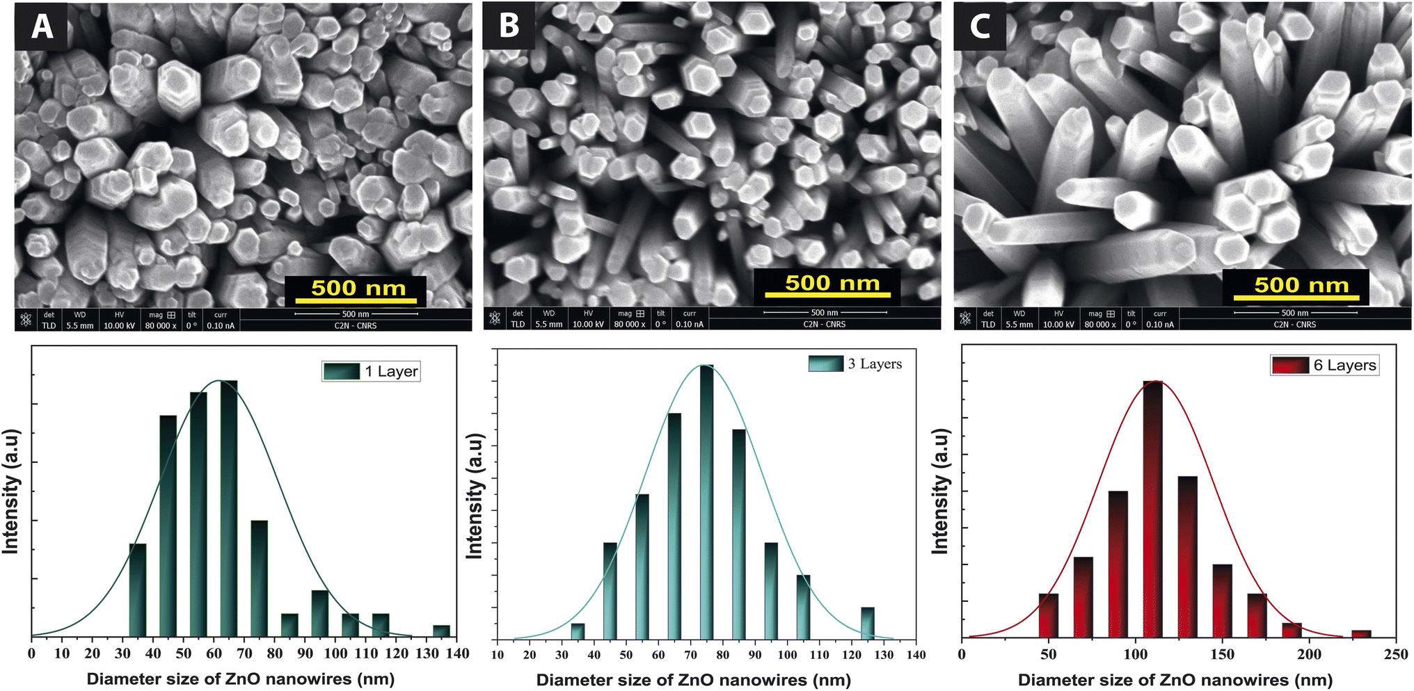 | ||
| Fig. 2 Top: SEM micrographs of ZnO nanowires grown on silicon substrate with (A) one buffer layer, (B) 3 buffer layers, (C) 6 buffer layers; below: the corresponding NWs diameter distribution obtained through the software ImageJ. | ||
Subsequently, we investigate the effects of the substrate on ZnO NWs deposited on a 100 nm thick buffer layer, using two types of ITO glass and Si substrates. As shown in Fig. 3, we observed that the growth of NWs is more compact on ITO substrate than on Si substrate. This can be explained by larger diameters of NWs on ITO, range from 260 nm to 640 nm. Due to this increase in the ZnO NWs diameter, the NWs density decreased from 68 nanowires per μm2 to 20 nanowires per μm2.
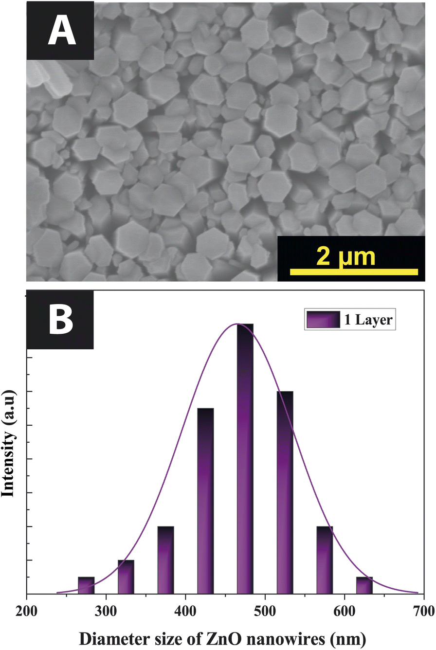 | ||
| Fig. 3 (A) SEM image and (B) diameter distribution of ZnO nanowires growth on ITO substrate. | ||
3.2 Optical properties of ZnO nanowires
The intensity of the Raman peaks is proportional to the quality of the material. The higher crystal quality of the material, the higher intensity and the narrower the peak width. Thus, crystallized ZnO has a much higher intensity than polycrystalline ZnO and amorphous ZnO. Raman spectra of ZnO NWs grown on Si and ITO substrates show vibrational modes attributed to a wurtzite structure of ZnO. Table 1 presents the experimental results regarding the position and full-width at half maximum (FWHM) of the Raman peaks.| ZnO NWs | Peak (cm−1) | FWHM (cm−1) | Vibration modes |
|---|---|---|---|
| Si | 96 | 4.19 | Elow2 |
| 435.74 | 10.24 | Ehigh2 | |
| 617.47 | 18 | TA + TO | |
| 668 | 20 | TA + LO | |
| ITO | 97.46 | 3.7 | Elow2 |
| 329.62 | 21.5 | Ehigh2 − Elow2 | |
| 381.67 | 3.7 | A1 (TO) | |
| 436.83 | 9.32 | Ehigh2 | |
| 569.32 | 54.43 | A1 (LO) | |
| 1101.36 | 66.24 | 2LO | |
| 1156.7 | 39.75 | 2A1 (LO) |
The positions of the lines and their widths at mid-height corresponding to the vibrational mode assignments are summarized in Table 3.11,19 The modes observed at 115, 300, 520 and 970 cm−1 are assigned to silicon substrate specific modes.21,22 As shown in Fig. 4A, a Raman line is detected around 437 cm−1, which is associated with the Ehigh2 of high intensity. These vibrational modes of ZnO NWs grown on an ITO substrate are more intense and a narrow mid-height width at 437 cm−1 than the vibrational modes of ZnO NWs grown on Si substrate. The latter seems relate a good crystalline quality of the ZnO/ITO NWs structure since the Ehigh2 mode is very sensitive to crystal lattice deformation under stress and the presence of defects.23
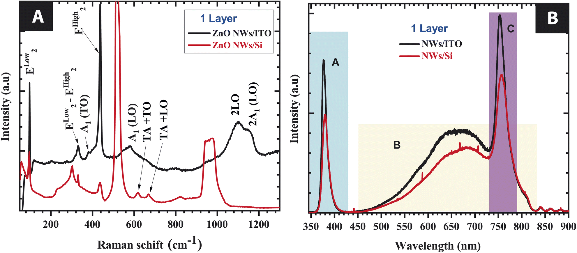 | ||
| Fig. 4 (A) Raman spectra, and (B) PL spectra of ZnO NFs grown on an ITO and Si substrate with 100 nm-thick of ZnO sol–gel thin film used as buffer layer. | ||
Nevertheless, Raman spectra, corresponding to the Ehigh2 − Elow2, is very weak for ZnO NWs. The detection of this mode is related to the presence of hydrogen in interstitial sites or oxygen vacancies in ZnO. Fig. 4B shows the photoluminescence spectra recorded in the wavelength range of 325 to 900 nm at room temperature under an excitation length of 325 nm. We observed that these spectra are mainly composed of two asymmetric bands: the exciton emission band in the UV range and a defect emission band in the visible range. The emission of these bands is more intense for the growth ZnO NWs on ITO than Si substrate.
As presented in Fig. 4B, the optical responses of ZnO NWs recorded by photoluminescence can be divided into three areas:
• Region A: in this region, the recombination emission near the zone edge (NBE) for ZnO NWs on ITO is more intense than Si substrate. These bands are located near 377 nm and 380 nm, respectively for ZnO grown on Si and ITO. For ZnO, the UV emission (also called near-band emission) is located near its absorption edge and which occurs through excitonic recombinations or band–band transitions. Excitons bound to dopants, native defects, or complexes produce extrinsic transitions that typically create discrete electronic states in the band gap.24
• Region B: the visible luminescence is usually a combination of emissions related to exciton transitions,25 surface defects, vacancies, and surface morphology.26
• Region C: the band in this region is centered around 754.5 nm, it is a second order response of the UV band (2λ = 2 × 377 = 754 nm).
We observe that the UV emission is more intense than the visible emission. This result seems to show the highest crystalline quality of ZnO.27 However the mechanism of PL in the visible region for ZnO is still far from being fully clarified.28
3.3 Structural properties of nanowires ZnO
In this paragraph we highlight the crystalinity properties of ZnO NWs by X-ray diffractogram analyses in terms of the influence of buffer layer thickness appear to agree with the observations of the SEM images, Raman and PL analysis. Fig. 5 shows the relationship between the nanowires and the possible growth orientation along the reticular plane (h k l). In general, the nanowires adopt the orientation (0 0 2) related to the thermodynamic energy at the surface.29 Due to the high deposition rate and associated energy, the adatoms at the surface (002), (100) and (101) are preferred planes leading to parallel growth with polycrystalline structure. The XRD shows a c-axis orientation leading to the hexagonal NWs being perpendicular to the substrate during the growth process, as shown in Fig. 5. And the result of SEM also confirms the columnar structure of ZnO. Fig. 5 shows that the c-axis does not grow perpendicular to the substrate, resulting in a polycrystalline structure of ZnO. Note that poorly aligned nanowires should be detected by XRD, which have the (100) and (101) preferred planes in addition to the (002) preferred plane. Moreover, peaks less intense than the peaks in the (0 0 2) plane are detected in the XRD diffractograms of the ZnO nanowires, and these peaks are related to the polycrystalline structure. We obtained a strong peak (002) that is related to the orientation of the ZnO NWs along the c-axis as seen in Fig. 6A. The identification of the peaks of the spectra obtained from the series of samples are in agreement with the data base sheet ICDD (International Center of Diffraction Data) of number 36-1451. These growth nanomaterials are single phase with hexagonal structure of wurtzite type. We highlight a strong preferential direction of growth along the c-axis, since line (002) at the diffraction line 2θ = 34° angle. The presence of peaks associated with the silicon substrate disappear when the thickness of the ZnO buffer layer increases. While, the intensities of the (1 0 0), (1 0 1), (1 0 2), (1 0 3), and (2 0 1) directions increase as the thickness of the buffer layer increases. These observed directions are probably due to the presence of the polycrystalline structure of the buffer layer. We have demonstrated successful growth by combining sol–gel and CBD synthesis, regardless of the substrate used, because ZnO NWs on ITO have a preferential crystalline plane as well (002). There is no discernible difference between the XRD patterns in Fig. 7B, as both graphs show the same peaks. In fact, both ZnO NWs growth on Si and ITO substrate are crystallized under a hexagonal structure of the wurtzite type.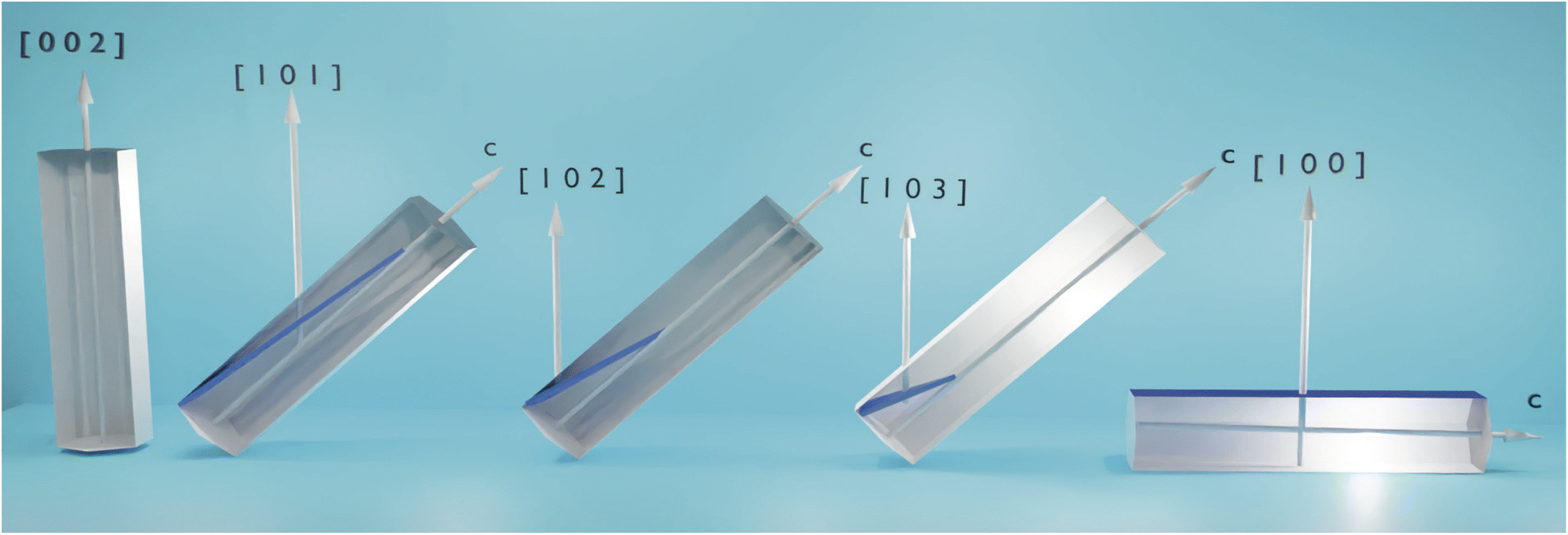 | ||
| Fig. 5 The orientation of the nanowires in the (h k l) planes with respect to the substrate plane. | ||
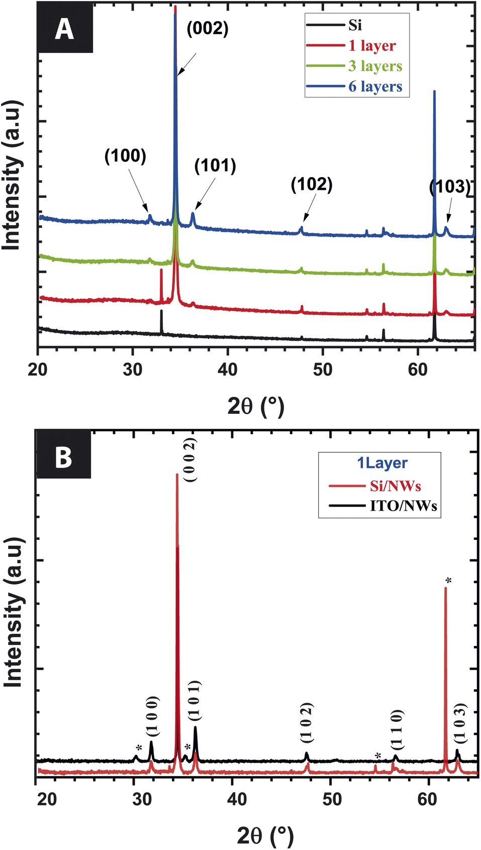 | ||
| Fig. 6 XRD pattern of ZnO NWs growth (A) on silicon substrate covering with buffer layer of varying thickness, and (B) on ITO substrate with one buffer layer (100 nm thick). | ||
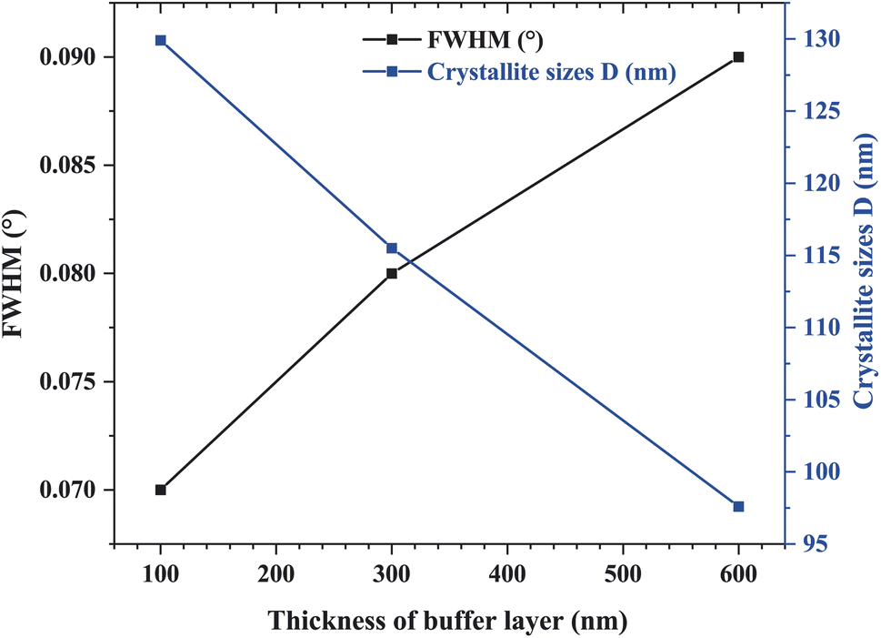 | ||
| Fig. 7 FWHM and crystallite size of the ZnO NWs as a function of buffer layer thickness. | ||
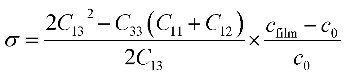
In the following, we show that the properties of the stress (σ) can be very strongly influenced by the thickness of the buffer layer and the substrate, as shown schematically in Fig. 1. The stress and lattice parameters a, c, and the c/a ratios of ZnO NWs grown on Si substrate as function on buffer layer thickness are summarized in Table 2.
| Number of buffer layers | a = b (Å) | c (Å) | c/a | σ (GPa) |
|---|---|---|---|---|
| 1 (100 nm) | 3.264 | 5.23 | 1.602 | −0.235 |
| 3 (300 nm) | 3.275 | 5.243 | 1.600 | −0.263 |
| 6 (600 nm) | 3.278 | 5.244 | 1.600 | −0.317 |
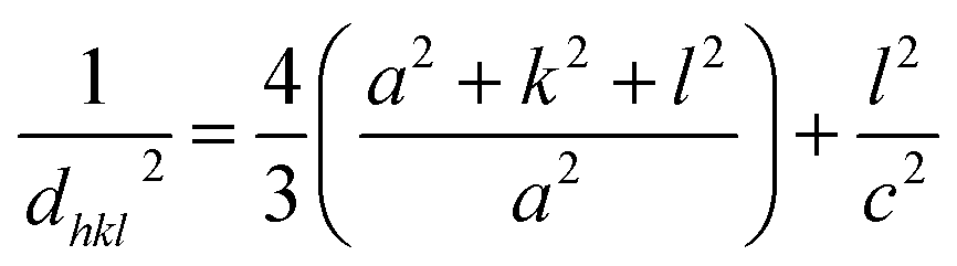
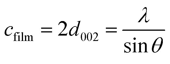
These lattice parameters a and c were calculated by using the relation of dhkl following the eqn (7) and (8):20
 | (7) |
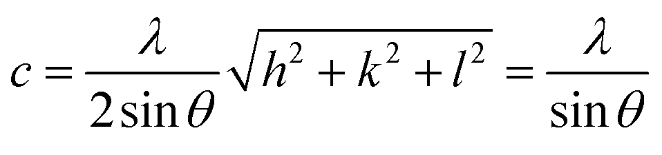 | (8) |
 | (9) |
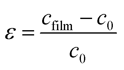
The stress σ values in our synthesis of ZnO NWs were estimated from the observed shift, in the diffraction peak between their positions in the XRD spectra via the formula, which is valid for a hexagonal lattice:
 | (10) |
 | (11) |
 | (12) |
| σ = −233 × ε | (13) |
We obtained a compressive stress, range from −0235 GPa to −0.317 GPa, that increases with the number of the buffer layer. This is explained by the presence of defects in the buffer layer and the growth of ZnO NWs, as shown in Fig. 4 PL spectra in region B in the wavelength range from 500 nm to 700 nm. We have shown that PL analysis can be a useful tool to determine the defects in ZnO NWs, allowing a better interpretation of X-ray analysis.
The effects of a thicker buffer layer on the growth of ZnO NWs on the Si substrate were then compared with the ITO substrate. The stress values for ZnO NWs/Si and ZnO NWs/ITO, grown on 6 buffer layers of ZnO sol–gel thin film with a thickness of about 600 nm, are shown in Table 3. It can be seen that the two stresses of the two samples are different. The stress value of ZnO NWs/ITO is positive, which means that the stress is in tension (extensive) direction. On the other hand, the sign of the stress value of ZnO NWs/Si was negative, which means that it is compressive stress. This contradiction is probably due to the relaxation phenomenon at the interface between the substrate and the buffer layer. Indeed, numerous defects such as dislocations and even net shifts can occur at the interface, which are relatively important. These effects seem to affect less the quality of ZnO NWs on ITO substrate.
| Samples | FWHM | D (nm) | δ (10−4 nm−2) | σ (GPa) |
|---|---|---|---|---|
| ZnO NWs/Si | 0.093 | 97.9 | 1.043 | −0.317 |
| ZnO NWs/ITO | 0.071 | 132 | 0.574 | 0.269 |
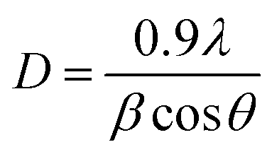
Table 2 summarizes the crystallite sizes, dislocation density, and FWHM of ZnO NWs grown on ITO and Si. For a thicker buffer layer, we observed that the FWHM of ZnO NWs on ITO substrate is lower than that of ZnO NWs on Si substrate. This indicates that the ZnO NWs/ITO are more crystallized and oriented along the c-axis than the ZnO NWs/ITO. According to the studies of M. Ali Yildirim et al., the crystallite size is large when the FWHM value of the (002) peak is low, therefore, the dislocation density value is also low and the obtained layer is better crystallized.31 The dislocation density is expressed as follows:32
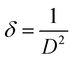 | (14) |
This layer dislocation density (δ) is a parameter corresponding to the dislocation line length per unit volume of the crystal and represents the imperfection of the crystal lattice. Indeed, dislocations are non-equilibrium imperfections in contrast to vacancies (O2−) or interstitial atoms (Zn2+). Moreover, dislocation density (δ) represents defects in crystal growth due to mismatch of the lattice between the substrate and the deposition of materials in the form of nanostructures or impurities. The value of the layer dislocation density (δ) is inversely proportional to the square of the crystal size. In our work, the crystallization of the hexagonal phase of ZnO NWs grown were obtained on Si, as well as ITO substrate. ZnO NWs grown on ITO with 6 buffer layers, have a crystallite size value evaluated at 132 nm and a very low dislocation density of 1.662 × 10⁻⁴ nm−2 for a FWHM of about 0.093°. As expected, we find that the crystallite sizes of ZnO NWs grown on ITO substrate are larger than those grown on Si substrate. In the (0 0 2) plane, these values vary from 132 nm for ZnO NWs/ITO to 97.9 nm for ZnO NWs/ITO following a decrease in FWHM values corresponding to a narrower and more intense peak as seen in Fig. 6.
In this study, Raman, and PL spectroscopy have been shown to be a more sensitive technique than XRD for investigating structural changes due to the presence of defects in ZnO NWs.
4 Discussion
The objective of this study is to fabricate c-oriented ZnO nanowires with preferential (002) planes on a sol–gel ZnO buffer layer of different thicknesses deposited by spin-coating. Azmi et al.17 was reported that increasing the buffer layer thickness, from 14.43 nm to 53.13 nm, improves crystallinity ZnO nanowires growing from planes (100), (002), (102), (110), and (103), (101), (102), (110), and (103), and preferential growth occurs at the (101) planes.17Herein, we demonstrated the influence of the presence of the buffer layer range from 100 nm to 600 nm on the growth of ZnO NWs. As observed in Fig. 2, for a silicon substrate with a buffer layer we notice the good uniformity of ZnO NWs, while, without a buffer layer, we observed the presence of nanoflowers. These nanoflowers are not uniform and do not cover the whole substrate. These latters not adhere properly and easily detached from the substrate. Although the presence of the relatively rough buffer layer, the latter allows the growth of nanowires fixed to the substrate and with a good rigidity. Moreover, the ratio c/a = 1.6 indicates that the lattice is compact. Indeed, this buffer layer plays the role of a seed layer, which is necessary for the growth of zinc oxide nanowires by chemical way. This control of the previously developed and studied thin films will allow a better control of the nanowire growth parameters.15,20 ZnO NWs have almost the same band gap with ZnO film but a much larger thickness-surface area ratio compared to spin-coating deposition. The results show that ZnO NWs have different morphologies, structures, and optical properties, proving that the buffer layer strongly influences the growth and properties of ZnO nanostructures.
Like silicon materials, indium tin oxide (ITO) is a key component in various applications such as photovoltaics due to its high optical transparency in the visible range (80%) and low electrical resistance (10−4 cm).33 In a real environment, sunlight can be quite diffuse. Solar cells must be very efficient at absorbing light in a wide range of wavelengths and at different angles of incidence. Overall, the structure of a solar cell based on ZnO nanowires has the advantage of capturing light better and increasing its efficiency. Herein, the SEM images show a network of hexagonal intertwined nanowires with different diameters. The advantage of smaller diameter nanowires is that they are better at absorbing short wavelength light, while larger diameter nanowires are more efficient for trapping light with longer wavelengths.
As observed in Tables 2 and 3, there are a large number of causes of residual stresses, such as the difference between the constants of thermal expansion coefficients, lattice mismatch in different materials, dislocations, incorporation of impurities, thickness of the deposited layer, etc. As the thickness of the deposited buffer layer increases, the residual stress changes. A slight change in compressive stress is seen as the thickness of the layer is increased. During the deposition of the material, sufficient kinetic energy is likely to be supplied to the atoms in the layer surface so that the atoms arrange on the substrate surface and cause compressive residual stresses. The surface energy is another parameter that can cause residual stresses. The surface energy of Si is nearly 1240 mJ m−2,34,35 while the surface energy of ITO glass is less than 100 mJ m−2.36,37 This means that Si substrates are more hydrophobic than ITO glass substrates. The quality of buffer layer deposited on ITO glass substrates is better than Si substrates. Since Si substrates are more hydrophobic, the buffer layer affects the growth of nanowires. Wang et al., reported that when the surface energy is decreased, the stresses increase and change their sign from negative to positive.38
As shown in Fig. 8, the reflectivity spectrum of ZnO nanowires deposited on Si wafer with 1 buffer layer and 3 buffer layers. We find that the decrease in light reflectivity from 2.96% to 0.58% for 1 buffer layer and 3 buffer layers respectively. We haven't measured the presence of the reflectivity spectrum of ZnO NWs grown on 6 buffer layers, because for this type of buffer layer seems to relate a reflectivity becomes 0%. This result is consistent with the SEM images because as the number of buffer layers increases, the orientation rate of nanowires on the substrate decreases, that means there is a low percentage of tilted nanowires. The increasing presence of wrinkles in the ZnO thin film sol–gel used as a buffer layer seems to affect the nanowire density and leads to surfaces with low nanowire density depending on the thickness of this layer. The tilt of the nanowires is the solution to decrease the reflectivity rate. Moreover, with this tilt, our samples can absorb all directions of light. Our previous work20 shows that we can decrease the reflectivity rate up to 9% with surface wrinkles. However, with ZnO NWs, we can decrease it to 2% (instead of 16% without nanowires) for one buffer layer and to 0% for 6 buffer layers. We also observe the presence of interference fringes whose amplitude decreases with the increase of the buffer layer. These fringes are due to the reflection of light between the substrate and the nanowires. The results of this study show that ZnO NWs are suitable candidates for applications based on light absorption, such as solar cells. Based on the optical characterization, it was shown that these materials can be used as a window layer in solar cells as well as an antireflection layer to absorb light radiation or as a UV sensor. ZnO nanowires are piezoelectric materials and this has already been demonstrated by the strong alignment of the peak (0 0 2), which shows that the ZnO nanowires are well aligned along the c-axis. Thus, based on this result, these materials can be used in energy harvesting applications.
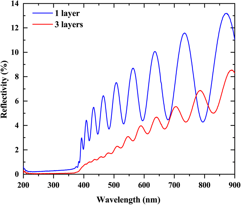 | ||
| Fig. 8 The reflectivity spectrum of ZnO NWs grown on a Si substrate with one buffer layer and 3 buffer layers. | ||
5 Conclusions
Highly oriented (002) ZnO nanowires has been successfully grown by chemical bath deposition in this study. The characterization of the ZnO NWs was investigated by SEM, Raman, PL, XRD, and reflectometer. The influence of ZnO sol–gel thin-film used as the buffer layer on morphological, optical properties and structural properties were studied. It was found that the buffer layer affect the formation of ZnO NWs. Crystallinity of the ZnO NWs is also confirmed using XRD, which the results shows that the increase of buffer layer increases the intensity of (002) orientation.Author contributions
E. H., N. B. M. and, M. L. conceived the study. N. B. and E. H. constructed the experiment, performed the measurement. All the authors analysed the data, and discussed the results E. H. and N. B. M. and co-wrote the paper.Conflicts of interest
There are no conflicts to declare.Acknowledgements
The authors thank the staff of the clean room and characterization laboratory of C2N, and CRTEn. This work was partially supported by the French RENATECH network of technological facilities.Notes and references
- D. M. Cruz, E. Mostafavi, A. Vernet-Crua, H. Barabadi, V. Shah, J. L. Cholula-Díaz, G. Guisbiers and T. J. Webster, JPhys Mater., 2020, 3, 034005 CrossRef CAS
.
- Y. Q. Fu, J. Luo, N.-T. Nguyen, A. Walton, A. J. Flewitt, X.-T. Zu, Y. Li, G. McHale, A. Matthews and E. Iborra, et al., Prog. Mater. Sci., 2017, 89, 31–91 CrossRef CAS
- E. Herth, L. Valbin, F. Lardet-Vieudrin and E. Algré, Microsyst. Technol., 2017, 23, 3873–3880 CrossRef CAS
- E. Herth, D. Fall, J.-Y. Rauch, V. Mourtalier and G. Guisbiers, J. Mater. Sci.: Mater. Electron., 2020, 31, 4473–4478 CrossRef CAS
- E. Herth, E. Algre, J.-Y. Rauch, J.-C. Gerbedoen, N. Defrance and P. Delobelle, Phys. Status Solidi A, 2016, 213, 114–121 CrossRef CAS
- Q. C. Bui, G. Ardila, E. Sarigiannidou, H. Roussel, C. Jiménez, O. Chaix-Pluchery, Y. Guerfi, F. Bassani, F. Donatini, X. Mescot, B. Salem and V. Consonni, Appl. Mater. Interfaces, 2020, 12, 29583–29593 CAS
- C. V. Manzano, L. Philippe and A. Serrà, Crit. Rev. Solid State Mater. Sci., 2022, 47, 772–805 CrossRef CAS
- C. Yin, J. Wu, J. Zhou, D. Zhang, Z. Liu, X. Liu, L. Liu, Z. Zhan, S. Garner and Y. Fu, Sens. Actuators, A, 2021, 321, 112590 CrossRef CAS
- N. Smagin, L. Djoumi, E. Herth, M. Vanotti, D. Fall, V. Blondeau-Patissier, M. Duquennoy and M. Ouaftouh, Sens. Actuators, A, 2017, 264, 96–106 CrossRef CAS
- J. Sultana, S. Paul, R. Saha, S. Sikdar, A. Karmakar and S. Chattopadhyay, Thin Solid Films, 2020, 699, 137861 CrossRef CAS
- M. Wlazło, M. Haras, G. Kołodziej, O. Szawcow, J. Ostapko, W. Andrysiewicz, D. S. Kharytonau and T. Skotnicki, Materials, 2022, 15, 6767 CrossRef PubMed
- Z. L. Wang and J. Song, Science, 2006, 312, 242–246 CrossRef CAS PubMed
- L. Serairi and Y. Leprince-Wang, Crystals, 2022, 12, 1023 CrossRef CAS
- A. Hamdi, A. Hamieh, M. Alamri, K. Dogheche, M. M. S. Mohan, R. Desfeux, D. Remiens and E. Dogheche, Surf. Interfaces, 2022, 31, 102103 CrossRef CAS
- N. B. Moussa, M. Lajnef, N. Jebari, F. Mahut, C. Villebasse, X. Lafosse, C. David, J. Chaste, R. Chtourou and E. Herth, Phys. Status Solidi A, 2022, 219, 2100480 CrossRef CAS
- J. Song and S. Lim, J. Phys. Chem. C, 2007, 111, 596–600 CrossRef CAS
- Z. H. Azmi, S. N. Mohd Aris, S. Abubakar, S. Sagadevan, R. Siburian and S. Paiman, Coatings, 2022, 12, 474 CrossRef CAS
- S. Paul, A. Das, M. Palit, S. Bhunia, A. Karmakar and S. Chattopadhyay, Adv. Mater. Lett., 2016, 7, 610–615 CrossRef CAS
- C. Lausecker, B. Salem, X. Baillin and V. Consonni, Nanomaterials, 2022, 12, 1069 CrossRef CAS PubMed
- N. B. Moussa, M. Lajnef, N. Jebari, C. Villebasse, F. Bayle, J. Chaste, A. Madouri, R. Chtourou and E. Herth, RSC Adv., 2021, 11, 22723–22733 RSC
- I. E. Tyschenko, V. A. Volodin and V. P. Popov, Semiconductors, 2019, 53, 493–498 CrossRef CAS
- W.-J. Lee and Y.-H. Chang, Coatings, 2018, 8, 431 CrossRef
- X. Zhu, H. Wu, Z. Yuan, J. Kong and W. Shen, J. Raman Spectrosc., 2009, 40, 2155–2161 CrossRef CAS
- A. C. García-Velasco, A. Báez-Rodríguez, M. Bizarro, L. García-González, J. Hernández-Torres and L. Zamora-Peredo, Nanotechnology, 2020, 31, 205601 CrossRef PubMed
- R. R. Jalolov, S. Z. Urolov, Z. S. Shaymardanov, S. S. Kurbanov and B. N. Rustamova, Mater. Sci. Semicond. Process., 2021, 128, 105783 CrossRef CAS
- S. Nadupalli, S. Repp, S. Weber and E. Erdem, Nanoscale, 2021, 13, 9160–9171 RSC
- A. Galdámez-Martinez, G. Santana, F. Güell, P. R. Martínez-Alanis and A. Dutt, Nanomaterials, 2020, 10, 857 CrossRef PubMed
- N. A. Althumairi, I. Baig, T. S. Kayed, A. Mekki, A. Lusson, V. Sallet, A. Majid and A. Fouzri, Vacuum, 2022(198), 110874 Search PubMed
- Y.-H. Hu, Y.-C. Chen, H.-J. Xu, H. Gao, W.-H. Jiang, F. Hu and Y.-X. Wang, Engineering, 2010, 2(12), 4 CrossRef
- L.-W. Ji, S.-M. Peng, J.-S. Wu, W.-S. Shih, C.-Z. Wu and I.-T. Tang, J. Phys. Chem. Solids, 2009, 70, 1359–1362 CrossRef CAS
- M. Ali Yıldırım and A. Ateş, Opt. Commun., 2010, 283, 1370–1377 CrossRef
- A. F. Abdulrahman, A. A. Barzinjy, S. M. Hamad and M. A. Almessiere, ACS Omega, 2021, 6, 31605–31614 CrossRef CAS PubMed
- F. Hamouda, E. Herth, C. David, F. Bayle, M. Plante, A. Martin and A. Aassime, J. Mater. Sci.: Mater. Electron., 2019, 30, 8508–8514 CrossRef CAS
- J. J. Gilman, J. Appl. Phys., 1960, 31, 2208–2218 CrossRef CAS
- A. Ramstad, G. Brocks and P. J. Kelly, Phys. Rev. B: Condens. Matter Mater. Phys., 1995, 51, 14504–14523 CrossRef CAS PubMed
- J. S. Kim, R. H. Friend and F. Cacialli, J. Appl. Phys., 1999, 86, 2774–2778 CrossRef CAS
- S. K. Rhee, J. Mater. Sci., 1977, 12, 823–824 CrossRef CAS
- G. Wang and X. Li, Appl. Phys. Lett., 2007, 91, 231912 CrossRef
| This journal is © The Royal Society of Chemistry 2023 |