
 Open Access Article
 This Open Access Article is licensed under a Creative Commons Attribution-Non Commercial 3.0 Unported Licence
Photoelectrochemical properties of copper pyrovanadate (Cu2V2O7) thin films synthesized by pulsed laser deposition†
Blandine Fontainea,
Youssef Benrkiaa,
Jean-François Blach a,
Christian Mathieua,
Pascal Rousselb,
Ahmad I. Ayeshc,
Adlane Sayedea and
Sébastien Saitzek*a
a,
Christian Mathieua,
Pascal Rousselb,
Ahmad I. Ayeshc,
Adlane Sayedea and
Sébastien Saitzek*a
aUniv. Artois, CNRS, Centrale Lille, Univ. Lille, UMR 8181, Unité de Catalyse et Chimie du Solide (UCCS), F-62300 Lens, France. E-mail: sebastien.saitzek@univ-artois.fr; Fax: +33 321177955; Tel: +33 321791732
bUniv. Lille, CNRS, Centrale Lille, Univ. Artois, UMR 8181, Unité de Catalyse et Chimie du Solide (UCCS), F-59000 Lille, France
cPhysics Program, Department of Math. Stat. and Physics, College of Arts and Sciences, Qatar University, P. O. Box: 2713, Doha, Qatar
First published on 19th April 2023
Abstract
Polymorphic phases of copper pyrovanadate (α- and β-Cu2V2O7) were synthesized by solid state reaction and the mechanisms governing the phase transitions have been highlighted by the ThermoGravimetric Analysis (TGA) and the Differential Scanning Calorimetry (DSC). The thermal evolution of the lattice parameters was determined by high temperature X-ray Diffraction revealing negative thermal expansion coefficients. The thermogravimetric analysis coupled with differential scanning calorimetry was also used to determine the optimal conditions to obtain a dense target in order to produce thin films by the Pulsed Laser Deposition (PLD) technique. Thin films elaborated under different oxygen pressures and temperatures exhibit a β-Cu2V2O7 polycrystalline phase and their band gap indicates absorption in the visible range. These oxides can be used as photoanodes and their photoelectrochemical properties were studied for both bulk (α-Cu2V2O7) and thin films (β-Cu2V2O7), as a function of the wavelength and/or intensity of the luminous flux. The best photocurrent efficiency was obtained under 450 nm illumination. Moreover, in the case of thin films, we have observed a linear evolution of the current density with the luminous flux. Finally, the photostability of thin films was measured and shows a reduction in the photocurrent of 8% after 1 h of measurement. This photocorrosion phenomenon was also highlighted by the elemental mapping performed on thin films by Scanning Electron Microscopy (SEM) coupled with Energy Dispersive X-ray Spectrometry (EDS).
1. Introduction
For many years, research on materials that can convert solar energy into electrical/chemical energy represents a tremendous scientific and societal challenge. The main objective is to produce energy devices with good conversion efficiency and with eco-responsible energy sustainability. Today, several devices exist to meet these challenges allowing a conversion of solar energy into electrical or chemical energy (H2): photovoltaic cells, photocatalysts for water splitting, Photo-Electrochemical Cells (PEC), etc.…1,2 In these devices, the use of efficient photo-active materials in terms of both absorption of light energy and conversion efficiency is essential. For this, a great deal of research has already been carried out on the use of semi-conductor oxides such as ZnO or TiO2.3 These oxides have a high chemical stability and are relatively inexpensive, which are advantageous for large-scale industrial production. Nevertheless, it has been shown in the literature that best materials must absorb the maximum visible light and their band gap must be between 1.8 and 2.4 eV.4,5 Consequently, to be effective in visible light, the oxides described above must be combined with another absorbing compound in order to allow efficient conversion in the visible range. For example, TiO2 can be associated with an organic dye in order to design solar cells called dye-sensitized solar cells or associated with another semiconductor to create n/p hetero-junctions, as TiO2/Cu2O to design all-oxide solar cells.6 Of course, the absorption is not the only criterion, the efficiency of materials will also depend on their intrinsic properties to separate charges with a good balance between transfer and recombination rate. The diffusion length and the carrier's lifetime can also be conditions limiting the conversion efficiency.7Today, many ternary metal oxides are studied for applications as photoelectrodes because they have suitable bandgaps and bands edge positions for being used in water-splitting photoelectrochemical tandem cells under solar irradiation. Among these ternary metal oxides, there are main families such as spinels (CuFe2O4,8 CaFe2O4,9…), delafossite-type oxides (CuFeO2,10 AgRhO2,11…), perovskites (LaFeO3,12 BiFeO3,13…) and many others.14 Copper pyrovanadate (Cu2V2O7) oxides is also promising candidates for the design of photo-electrodes which can be used in PEC cells. For example, Guo et al.15 obtained a current density of 12 μA cm−2 (at 1.23 V vs. NHE) on thick films of β-Cu2V2O7 produced by the drop-casting technique in 0.1 M sodium borate buffer solution. However, these properties can be improved by controlling the microstructure of the oxide. Thus, Khan et al.16 highlighted a significant improvement in current density (0.70 mA cm−2) for thick films made up of micro-flakes arranged in channels; C. Gadiyar et al.17 indicated a current density of 0.23 mA cm−2 (always at 1.23 V vs. NHE) in 0.1 M sodium borate buffer solution (pH = 9.2) containing 0.1 M Na2SO3 as a hole scavenger. Their study shows an optimal crystallite size at 40 nm corresponding to the hole diffusion length, estimated between 20 and 40 nm.18 Copper pyrovanadates (α- or β-Cu2V2O7 oxides) have also been studied for other applications, in particular for: (i) magnetoelastic and ferromagnetic coupling properties; (ii) ferroelectric properties induced by a magnetic order;19 (iii) photo-degradation properties of azo-dye in water;20,21 (iv) solar water splitting;22,23 (v) catalytic SO3 decomposition;24 (vi) cathode materials in high voltage Li-batteries.25–27
Copper pyrovanadate oxides have three polymorphic phases: (i) α-Cu2V2O7 (blossite) has an orthorhombic structure with Fdd2 space group and lattice parameters: a = 20.68 Å, b = 8.411 Å and c = 6.448 Å;28 (ii) β-Cu2V2O7 (ziesite) crystallizes in a monoclinic structure with A2/a space group and lattice parameters: a = 10.094(15) Å, b = 8.020(13) Å, c = 7.711(10) Å and β = 110.43(9)°;29 (iii) γ-Cu2V2O7 (observed at high temperature in the range of 710 °C to 780 °C) has a triclinic structure with P![[1 with combining macron]](https://www.rsc.org/images/entities/char_0031_0304.gif) space group and the following lattice parameters: a = 5.0873(10) Å, b = 5.8233(11) Å, c = 9.4020(18) Å, α = 99.780(3)°, β = 97.253(3)°, γ = 97.202(3)°.30 Under normal pressure and temperature conditions, α- or β-Cu2V2O7 phase can be synthesized. For example, the reaction between V2O5 and CuO, at low temperature (T < 550 °C), lead to the stabilization of β-Cu2V2O7. While for syntheses at higher temperature (T > 560 °C), α-Cu2V2O7 phase will be privileged.31 However, fairly long calcination times are required,32 to achieve a pure phase. The β-Cu2V2O7 → α-Cu2V2O7 phase transition takes place around 605 °C. However, the β-Cu2V2O7 phase can also be obtained from α-Cu2V2O7 phase by heating it up to 710 °C and then performing a rapid cooling. In this case, the phase transition process is as follows: α-Cu2V2O7 → γ-Cu2V2O7 → β-Cu2V2O7.31
space group and the following lattice parameters: a = 5.0873(10) Å, b = 5.8233(11) Å, c = 9.4020(18) Å, α = 99.780(3)°, β = 97.253(3)°, γ = 97.202(3)°.30 Under normal pressure and temperature conditions, α- or β-Cu2V2O7 phase can be synthesized. For example, the reaction between V2O5 and CuO, at low temperature (T < 550 °C), lead to the stabilization of β-Cu2V2O7. While for syntheses at higher temperature (T > 560 °C), α-Cu2V2O7 phase will be privileged.31 However, fairly long calcination times are required,32 to achieve a pure phase. The β-Cu2V2O7 → α-Cu2V2O7 phase transition takes place around 605 °C. However, the β-Cu2V2O7 phase can also be obtained from α-Cu2V2O7 phase by heating it up to 710 °C and then performing a rapid cooling. In this case, the phase transition process is as follows: α-Cu2V2O7 → γ-Cu2V2O7 → β-Cu2V2O7.31
In the literature, several synthetic routes are described, for example solid-state reaction,31 wet chemical method,21 Sol–gel synthesis,33 hydrothermal synthesis,34 thermal decomposition method35 and finally flux method in close crucible to obtain single crystals.36 In thin film form, studies are scarce and to the best of our knowledge only films produced by electrospraying,22 simplified Successive Ionic Layer Adsorption and Reaction (s-SILAR) method37 and drop casting method15 have been described.
In this present work, we studied the photoelectrochemical properties of Cu2V2O7 thin films synthesized by Pulsed Laser Deposition (PLD). The first part of the work, devoted to the synthesis of pure powder and the preparation of the PLD target will highlight the difficulties of obtaining a dense target. In the second part, and for the first time, we present the optimal conditions for the growth of thin films, in particular the influence of pressure and temperature. Finally, we will compare the photoelectrochemical properties of PLD-based thin films with bulk form.
2. Experimental section
Copper pyrovanadate powder was synthesized by solid-state reaction using copper oxide (CuO – 99.5% – strem chemicals) and ammonium vanadate (NH4VO3 – 99% – strem chemicals) precursors. These precursors were weighed in stoichiometric proportions and ground for 20 min to ensure a good homogeneity. Then, the mixture was calcined in an alumina crucible at 620 °C under air for 15 hours. The PLD target (1 in. diameter) was produced by pressing the Cu2V2O7 powder (15 kbar) in a circular uniaxial press, then by sintering the pellet. The thermal cycle consists of a ramp up/down in temperature at 4 °C min−1 and a step of 60 min at 720 °C.The thin films were synthesized by PLD technique using a Compex Pro 102 Laser (KrF excimer laser with a wavelength of 248 nm). The synthesis conditions are: 1.5 J cm−2 for the laser density energy, 4.5 cm for the target-substrate distance and 4 Hz for the pulse repetition rate. Before the deposition, a pre-ablation of 15 min is carried out in order to clean the target's surface.
The substrate temperature during deposition and the oxygen pressure are variable parameters studied in this work.
The structural properties of both powders and thin films were performed by X-Ray Diffraction (XRD) and Raman Spectroscopy. For the bulk form, the XRD patterns were recorded in the 15–70° range with a step of 0.02° and a scan speed of 0.4° per min, using a Rigaku Ultima IV X-ray diffractometer equipped with Cu anticathode (λKα = 1.5418 Å). Nickel foil filter and Soller slits are used to attenuate Cu Kβ radiation and to limit the divergence of X-ray beam, respectively. While the thermo-diffraction patterns were recorded on a D8 Bruker device. For the thin films, the XRD patterns were recorded using a Rigaku SmartLab diffractometer attached to a 9 kW rotating anode X-ray generator (λKα1 = 1.54056 Å) and monochromatized with a double Ge (220) monochromator. Raman spectra were recorded in back scattering geometry using a Horiba Labram HR800 spectrometer coupled with a microscope which focused the 784 nm laser beam to a 1 μm spot. The spectra were recorded in the 100–1100 cm−1 range.
Thermal Analyses have been performed using a TGA/DSC3+ STARe System (Mettler Toledo). The sample was analyzed in the range 50 °C–750 °C with a rate of 10 °C min−1 under a flow of air of 50 mL min−1 in 70 μL Al2O3 crucible.
Infrared (IR) analysis was conducted using a Shimadzu IR Prestige 21 instrument with the addition of single-reflection diamond module (ATR). IR spectra were recorded in the range 500–4000 cm−1 with a 1 cm−1 resolution. A Nova made scanning electron microscope (SEM) model NanoSEM-450 was employed for investigation of morphology and grain size and the elementary maps were recorded with a Hitachi SU3800 SEM coupled with Energy Dispersive X-ray Spectrometry (EDS). The optical properties were characterized using a Shimadzu UV-visible spectrophotometer UV-2600 in the range of 190–800 nm with a resolution of 1 nm. This spectrophotometer was equipped with an integration sphere ISR-2600+, a photomultiplier tube and a InGaAs detector. The UV-visible diffuse reflectance spectra can be used to determine the optical gap band (Eg) using the Tauc plot defined by the following equation:
| αhν = A(hν − Eg)n | (1) |
The photoelectrochemical measurements were performed using a three-electrode cell (PEC 15 mL Redox.me®). The cell is calibrated for an illumination of 1 cm2 from the backside of the ITO/glass substrate (Delta Technologies, USA). The Pt wire was used as counter electrode and Ag/AgCl in saturated KCl electrode was employed as the reference electrode. The working electrode consists of a Cu2V2O7 deposited either by drop casting using the powder directly (a suspension of nanopowders is prepared in N,N-dimethylformamide/distilled water with the 1![[thin space (1/6-em)]](https://www.rsc.org/images/entities/char_2009.gif) :1 ratio, then annealed at 250 °C during 1 h in order to obtain a layer whose thickness is ∼50 μm) or by PLD technique.
:1 ratio, then annealed at 250 °C during 1 h in order to obtain a layer whose thickness is ∼50 μm) or by PLD technique.
The photoelectrochemical measurements were carried out using a PGSTAT204 potentiostat/galvanostat (Metrohm) expanded with Electrochemical Impedance Spectroscopy (EIS) module and coupled with optical bench consisting of highly focused LED source. The intensity of the light beam can be controlled as well as the excitation wavelength via the use of low spectral dispersion LEDs. The whole is controlled by NOVA 2.0 software. Finally, the electrolyte solution consists of 0.1 M sodium borate buffer solution also called NaBi Buffer (pH 9.2) with 0.1 M sodium sulfite as a hole scavenger. This electrolyte was used to preserve the chemical stability of Cu2V2O7 (ref. 38) and to improve the intensity of the collected photocurrent.39
3. Results and discussions
3.1 Bulk characterizations
The XRD pattern of Cu2V2O7 synthesized by solid state reaction is presented in Fig. 1a. This first result highlights the presence of a pure phase of α-Cu2V2O7 (Fdd2 space group). All the XRD lines can be indexed and the lattice parameters determined by least-squares refinement using MAUD software40 are: a = 20.688(3) Å, b = 8.410(7) Å and c = 6.449(1) Å. The Raman spectrum confirms the presence of a unique α-Cu2V2O7 phase with the characteristic vibrational modes (Fig. S1 – ESI†). D. De waal et al.41 have studied these modes for α and β phases. α-Cu2V2O7 has an orthorhombic structure with C192v symmetry in which the V2O74− group are nearly staggered. These anions group are located in parallel sheets bonded by Cu2+ cations.28 The VO3 stretching components are centered at 992, 920 (symmetric stretching) and 850 cm−1 (antisymmetric stretching). The VOV symmetric bridge stretch has a very low intensity at 553 cm−1 and at 790 cm−1.42 Therefore, one can conclude that the VO3 and/or OVO3 bending components are centered at 392, 254 and 111 cm−1.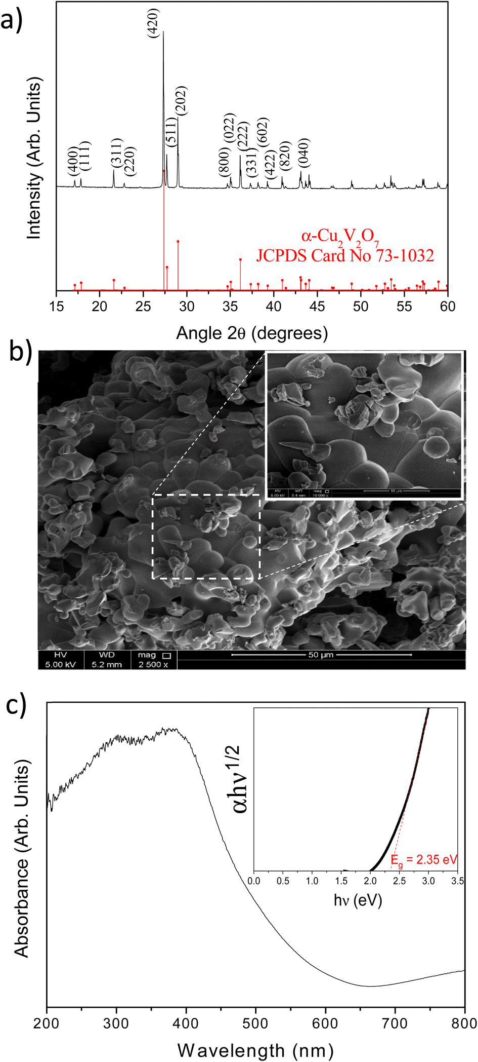 | ||
| Fig. 1 (a) XRD pattern of α-Cu2V2O7 as prepared and α-Cu2V2O7 reference; (b) SEM images of α-Cu2V2O7 powders; (c) absorbance spectrum of α-Cu2V2O7 (inset the calculated Tauc plot). | ||
The characteristic vibrational modes were also highlighted by IR spectroscopy using ATR configuration (Fig. S2 – ESI†). The bands located at 3330 and 1620 cm−1 are assigned to the traditional vibrations of OH stretching and bending vibration of adsorbed water molecules, respectively. The band centered to 993 cm−1 can be attributed to V–O stretching vibration and the band located around 700 cm−1 can be assigned to Cu–O bond. Moreover, the bands located between 750 cm−1 and 900 cm−1 can be assigned to the VO3 symmetric and asymmetric stretching vibrations.
The morphology of as prepared α-Cu2V2O7 is presented on SEM image (Fig. 1b). The powder has a granular morphology with a mostly spherical shape with heterogeneous size. The energy dispersive spectroscopy (EDS) confirms the correct stoichiometric ratio (% at. Cu/% at. V = 1) without heterogeneity.
The optical band gap energy was determined from the UV-visible absorption spectrum using Tauc method (Fig. 1c), knowing that α-Cu2V2O7 has an indirect band gap (n = 1/2).43 The determined value of the optical band gap is 2.35 eV (i.e. 528 nm). This value is particularly interesting because it is very close to the maximum intensity of the solar spectrum.
In order to prepare the PLD target, it is essential to study the Cu2V2O7 oxide stability by performing a thermal analysis by ThermoGravimetric Analysis (TGA) and Differential Scanning Calorimetry (DSC) measurements. For DSC, two heating/cooling thermal cycles are carried out between 50 °C to 750 °C with 10 °C min−1 and 20 °C min−1 rate, respectively. The results obtained are presented in Fig. 2a.
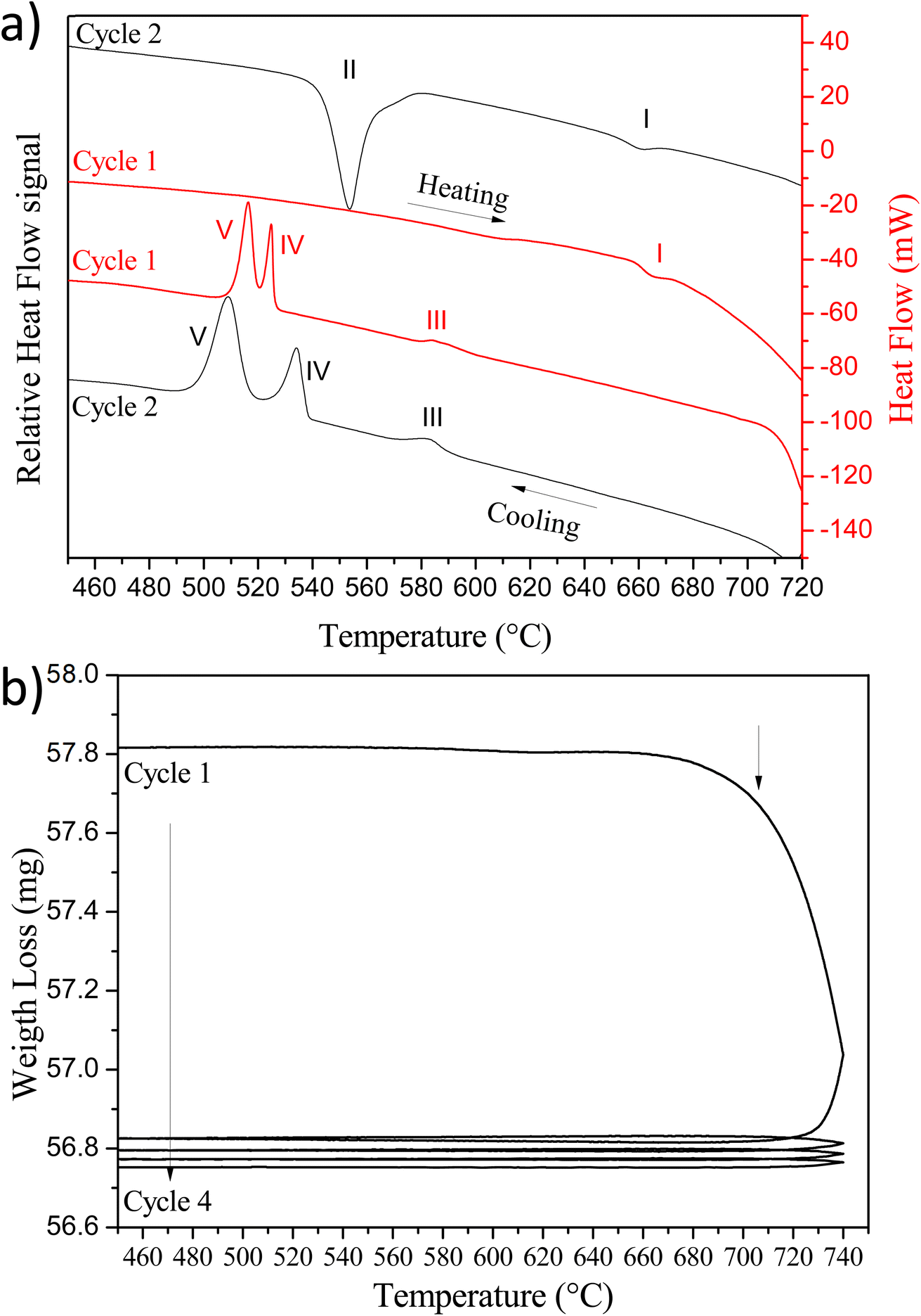 | ||
| Fig. 2 (a) DSC curves with two heating/cooling cycle with 10 °C min−1 (cycle 1) and 20 °C min−1 (cycle 2) performed on α-Cu2V2O7; (b) TGA measurements performed on four cycles showing the weight loss. | ||
During the first cycle, an endothermic peak (I) is observed on heating, attributed to α → γ phase transition (677 °C).44 Then, on cooling, three exothermic peaks appear. The first peak (III) corresponds to γ → β phase transition (∼595–600 °C). The two other peaks (IV and V) correspond to crystallization at low temperature of β-Cu2V2O7 phase. Indeed, B. V. Slobodin et al.44,45 indicates that above 720 °C, a small amount of CuVO3 is formed which forms an eutectic with the α and β phases having a low crystallization temperature.44 For the second cycle, a difference is observed. Indeed, the appearance of a new endothermic peak (II) is observed, which is related to the formation of β-Cu2V2O7 phase during the cooling step of the first cycle. This peak is attributed to β → α transition (557 °C). The second cooling step took place in the same way as that of the first cycle (the difference between peaks IV and V is only due to the different cooling rates thus confirming that it is an enthalpy of crystallization). The analysis of the weight loss with temperature presented in Fig. 2b, highlights the reduction of copper observed during the cooling step of the first cycle. The weight loss after 715 °C thus highlights a copper reduction (oxygen release) and the start of peritectic transformation around 770 °C. Indeed, above 725 °C, Cu2V2O7 undergoes a congruent fusion followed by an incongruous transformation towards 770 °C (peritectic decomposition).45
In order to understand this low crystallization temperature (IV and V peaks) due to the presence of the eutectic, additional measurements were undertaken but this time with a temperature limited to 720 °C. At this temperature, Cu2V2O7 phase is not reduced and therefore should not form eutectics. The TGA/DSC analysis cycles limited to 720 °C are shown in Fig. 3. As already observed by B. V. Slobodin et al.,44 the first heating step leads to the transformation α → γ at 705 °C (the XRD reference pattern is shown in Fig. S3 – ESI†). Then, the first cooling is accompanied by a release of heat due to the transformation γ → α → β. The second cycle shows an endothermic peak due to the transition from β → α at 604 °C (this peak is due to β-Cu2V2O7 which is formed during the first cooling), then comes the α → γ phase transformation, as during the first heating. The following cycles are similar and the crystallization peaks at low temperature are no longer observed, thus confirming the presence of an eutectic with the phase formed above 725 °C. This decomposition at a temperature higher than 725 °C is problematic because it limits the sintering temperature of the PLD target and therefore its densification.
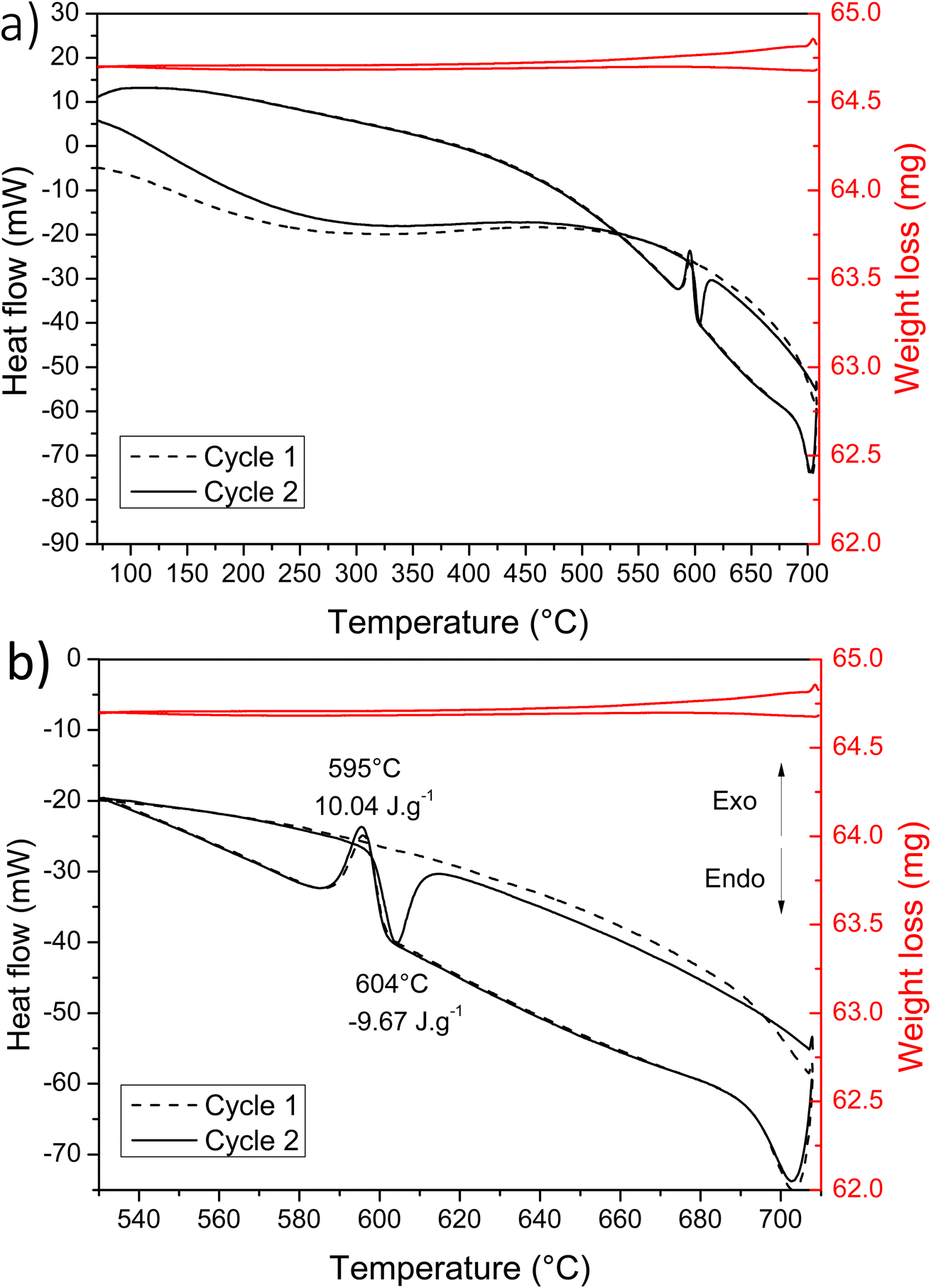 | ||
| Fig. 3 (a) DSC and TGA measurements realized with two heating/cooling cycles; (b) fragment of the curves highlighting the observed transitions. | ||
To confirm this behavior, in situ high temperature X-ray diffraction was performed over the temperature range 50 °C to 725 °C (heating/cooling in the same cycle). Fig. 4a shows a partial 2D map (XRD patterns vs. temperature) of α-Cu2V2O7 powder (the complete 2D map is presented in Fig. S4 ESI†).
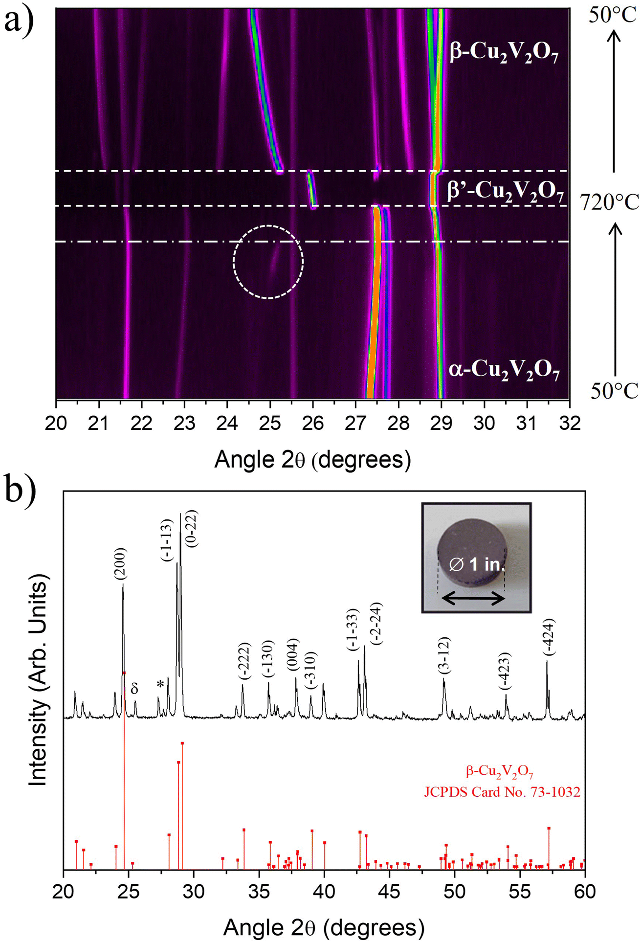 | ||
| Fig. 4 (a) Fragment of 2D map of thermo-diffraction patterns for heating/cooling cycle between 50 °C to 725 °C (δ indicates a reflection of the sample holder) and (b) XRD pattern of β-Cu2V2O7 as prepared and β-Cu2V2O7 reference (inset photograph of the PLD target). δ and * indicate the sample holder reflection and α-Cu2V2O7 phase, respectively. | ||
Initially, the presence of a pure α phase is observed. When the temperature increases, some diffraction peaks shift towards the large angles (as shown in Fig. S5 – ESI†), highlighting the presence of a negative Coefficient of Thermal Expansion (CTE).46 This shift is not identical according to the crystallographic planes. This reflects an anisotropic evolution of the unit cell as a function of temperature.47
Around 710 °C, a phase transition is observed (dashed lines in Fig. 4a). This transition corresponds to the transformation of the α phase towards a phase which can be attributed to the Cu1.98V1.96O6.92 phase with C2/c space group, previously described by S. A. Petrova et al.48 and called β′-Cu2V2O7 (Fig. S7 – ESI†). The presence of this phase also explains the mass loss observed in the TGA (oxygen release and Cu2+ reduction) measurements and we can note that a slight part seems to have melted in the sample holder, as observed at the end of the DSC thermal cycle. During cooling, a phase transition is also observed from the β′-Cu2V2O7 phase to the β-Cu2V2O7 phase at 600 °C. This phase is then preserved when returning to room temperature. From a structural point of view, the β′ → β phase transition causes a decrease in the V–O–V angle and a slight expansion of the VO4 tetrahedra.48 Here, a discrepancy with the TGA/DSC thermal analysis has to be noted. In the literature, α → γ transition is observed around 700 °C (as described in the DSC analysis part). However, in this present case, the XRD patterns indicate unambiguously that the obtained phase is β′-Cu2V2O7 phase (Cu1.98V1.96O6.92). Consequently, the α → γ phase transition previously claimed is in fact a α → β′ transition. Thus, all of the ATG data can be re-interpreted in the same way but this time by replacing the γ phase by the β′ phase (structural evolution of Cu2V2O7 oxide is presented in Fig. S8 – ESI†).
Concerning β-Cu2V2O7, X-ray thermodiffractograms show a negative expansion behavior (as depicted in Fig. S9 and S10 – ESI†) which correlates with the literature.49 In addition, the dotted circles in Fig. 4a reveal the formation of a small amount of β-Cu2V2O7 from 500 °C then disappears around 600 °C (corresponding to the β → α transition as observed on the DSC curve in Fig. 3). In summary, a good correlation between DSC and HT-XRD experiments is highlighted shading some light on the complex thermo-structural behavior of copper vanadate.
Those results also make possible to define the optimal conditions for developing the PLD target. For sintering, the temperature is limited to 720 °C (start of melting of a small part of Cu2V2O7 oxide) which allows solidification/densification of the target which is necessary for the PLD technique. The α-Cu2V2O7 powder was then shaped into a pellet via uniaxial press (15 kbar), then sintered at 720 °C for 1 hour. To avoid the diffusion of the elements into the alumina plate, a platinum sheet was used during the sintering step. The pellet obtained is dark brown and the XRD pattern indicates as expected the presence of β-Cu2V2O7 phase (Fig. 4b). It is important to note that after use, this target remains stable in air for a few weeks and then starts to disintegrate gradually. This phenomenon can be explained by the negative thermal expansion coefficient which induces strong mechanical stresses when the target is subjected to temperature variations caused by the laser impact.
3.2 Thin film characterizations
The PLD target was used to develop thin films grown on ITO/glass substrates. Among all different parameters intervening in PLD synthesis, we chose to study two important parameters (dynamic oxygen pressure and substrate temperature) in this work. The laser pulse number is fixed at 6000 pulses, the target-substrate distance is fixed at 45 mm and the frequency/fluence of the laser are 4 Hz and 2 J cm−2. Films thickness, determined by spectroscopic ellipsometry, is 150 nm, i.e. a growth of 0.25 Å per pulse. Fig. 5a shows the evolution of XRD patterns as a function of substrate temperature under a fixed pressure of 10−3 mbar.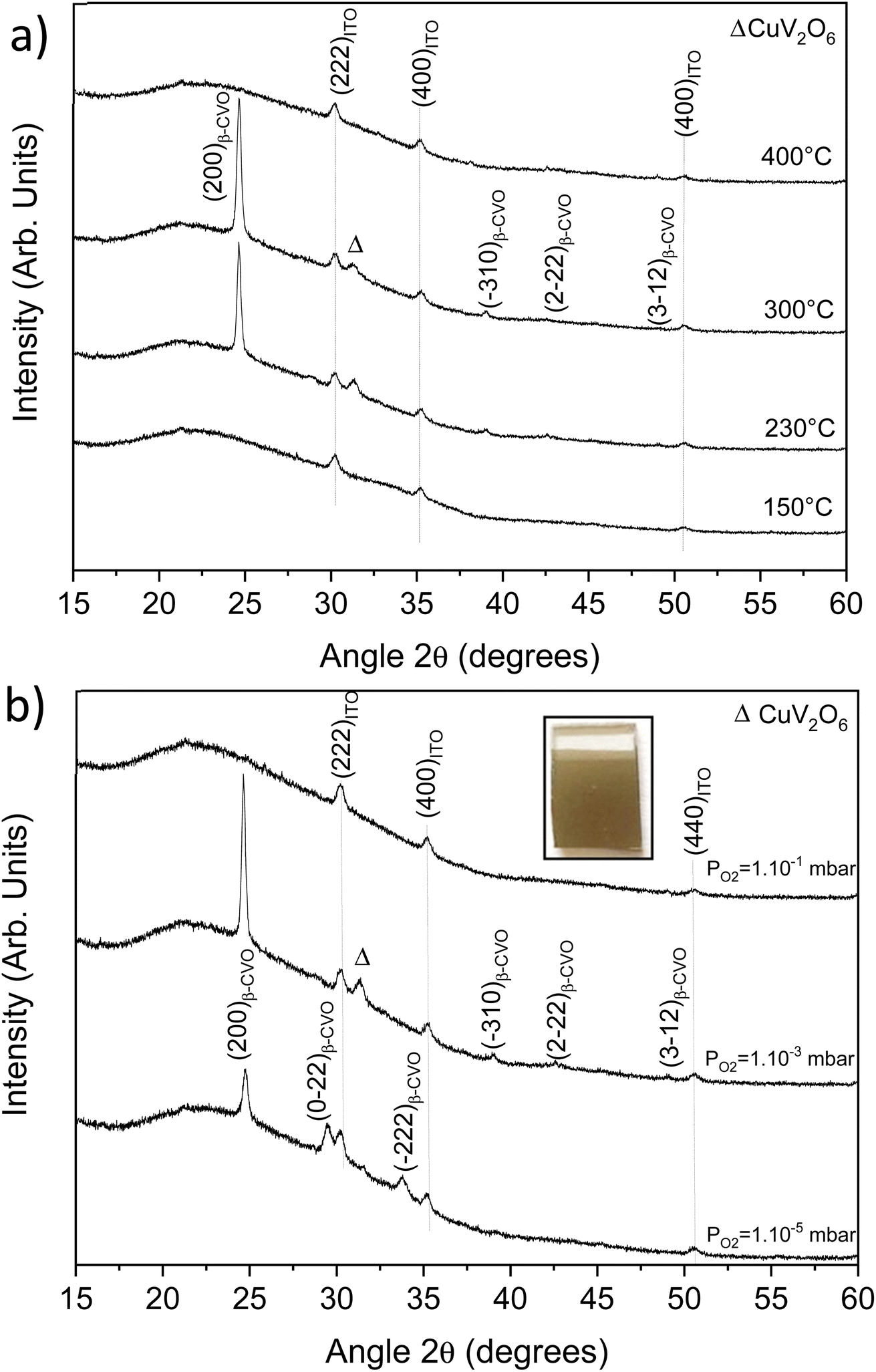 | ||
| Fig. 5 XRD patterns of copper vanadate thin film deposited on ITO/glass substrate vs. substrate temperature (a) and dynamic oxygen pressure (b) – (inset photograph of Cu2V2O7 thin film synthesized at 10−3 mbar of O2 pressure and 230 °C). | ||
The presence of a β phase with a (200) preferential orientation is highlighted for the temperatures of 230 and 300 °C. Note that a parasitic phase of CuV2O6 (legend with the Δ symbol) is also present at this pressure. At 150 °C and 400 °C, no reflection is highlighted except the reflections of Indium Tin Oxide (ITO). A temperature above 150 °C is necessary for the β-Cu2V2O7 crystallization. In addition, at high temperature also leads to the production of an amorphous thin film.
Thus, after setting the optimal temperature at 230 °C, we studied the influence of the dynamic oxygen pressure in the chamber. Fig. 5b shows the XRD patterns for different pressures. For thin film synthesized at 10−5 mbar, the pure β phase can be obtained but with the disappearance of the preferential orientation. At 10−3 mbar, a β phase is obtained but with the presence of a parasitic phase of CuV2O6 (Δ). For higher pressure (10−1 mbar), the (200) reflection of β-Cu2V2O7 goes out completely, indicating either the presence of an amorphous film or no film at all. The surface of the film synthesized at 10−1 mbar was thus analyzed by EDS at different points showing a homogeneous V/Cu ratio close to 1, in favor of the first hypothesis.
It should be noted that a freshly prepared target is necessary for the development of thin films and beyond ∼20 deposition cycles, the target crumbles, probably due to the negative expansion coefficient of the compound, under the effect of the thermal stresses induced by the laser impact.
As observed on Fig. S11 (ESI†), the lower oxygen pressure is, the lowest band gap is. This results in an increasingly dark appearance visible to the naked eye of the deposited film. Thus, the band gap evolves from 2.2 to 2.4 eV for 10−5 and 10−3 mbar, respectively. The photo-electrochemical measurements presented in next paragraph will be performed on the film elaborated at 10−5 mbar and at 230 °C. Indeed, these optimal parameters lead to a pure β-Cu2V2O7 phase (without CuV2O6 impurity).
3.3 Photoelectrochemical properties
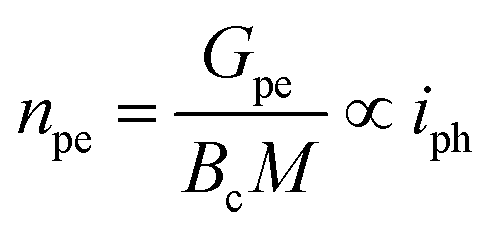
The photoelectrochemical performances of photoanodes were studied in a three-electrode cell (Ag/ACl as the reference electrode and Pt as the counter electrode) and in 0.1 M NaBi buffer solution. The chronoamperometry results achieved on α-Cu2V2O7 thick film are shown in Fig. 6a (in particular by plotting the variation of the current density between illumination and dark). A significant change in current density is observed when the backside of the working electrode is illuminated. In addition, one can note the variation of the photocurrent density (Δj) shows better efficiency towards low wavelengths. The variation being maximum at 450 nm with a photocurrent density of 0.45 μA cm−2 with an applied potential of 0.4 V vs. Ag/AgCl and ϕ0 = 23 mW cm−2 (while this drops to 0.11 μA cm−2 for 505 nm with the same luminous power). The evolution of the photocurrent with the intensity of luminous flux is presented in Fig. 6b showing a progressive evolution of the Δj according to the intensity received (Fig. 6c). The Δj vs. ϕ0 shows a two-step trend (dotted lines). Indeed, it follows a linear evolution (Δj = 1.92 × 10⁻³ϕ0) at first then evolves towards a power law (Δj = 0.16 × ϕ00.533). This crossover from 1 to ½ for the power of the luminous flux can be explained by the change of the dominant photocarrier decay mechanism from a trap-dominated recombination to an e–h recombination.50 Indeed, T. S. Moss51,52 indicates that the generation rate of photoelectrons by incident light (Gpe) follows the expression (2):| Gpe = Bcnpe(npe + M) ∝ ϕ0 | (2) |
 | (3) |
 | (4) |
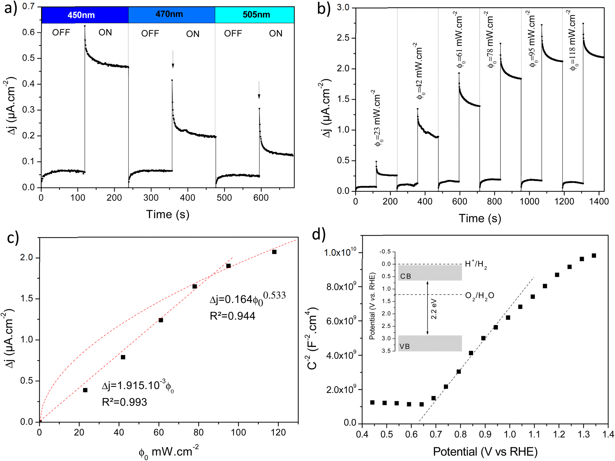 | ||
| Fig. 6 (a) Chronoamperometry (j–t) in dark and under illumination for different wavelengths with a constant light intensity of 23 mW cm−2; (b) difference in current density (Δj) under illumination or dark depending on the light intensity (450 nm) and with an applied potential of 0.4 V vs. Ag/AgCl; (c) Δj vs. ϕ0 plot and models in dotted lines; (d) Mott–Schottky plots for α-Cu2V2O7 film deposited on ITO/glass performed at 1 kHz (a borate buffer solution (pH = 9.2) was used as the electrolyte). | ||
Note that for higher intensities of the light beam, saturation can be achieved. This model therefore explains the experimental observations and the behavior of the electrode under different light power values.
The photocurrent transient response and especially the instantaneous pike and the subsequent decay towards the steady state current is due to the build-up of carriers in the surfaces states.53 Likewise, the current overshoot observed when the light is switched off is due to the recombination of the remaining carriers in the surface states. So, the charge transfer and the recombination rate constants can be obtained by modeling the transient photocurrent response.53,54 Indeed, the time constant of the decay or the overshoot is given by the expression (5):55
 | (5) |
Moreover, the ratio of the steady state photocurrent to the instantaneous photocurrent observed when the illumination is switched on is given by the expression (6):55
 | (6) |
These two expressions make possible to calculate the values of ktr and krec. Considering 450 nm illumination (ϕ0 = 23 mW cm−2), the values of ktr and krec are 6.19 × 10⁻² s−1 and 5.58 × 10⁻² s−1, respectively. The close values show that only half of the holes arriving at the surface are transferred to the solution under steady state conditions.
In addition, the capacitance versus potential (C–V) measurement is used to determine the conduction type, the flat band (Efb) and carrier density (N), which can be determined from the Mott–Schottky (MS) plot (1/C2 – V). Fig. 6d shows the MS plot of the β-Cu2V2O7 film performed at 1 kHz. The positive slope observed on the depletion zone indicates a n-type semiconductor behaviour. The Efb is estimated at −0.08 V (vs. Ag/AgCl) which correspond to 0.66 V (vs. RHE). This value is consistent with the values described in the literature.15 The flat band potential reflects the position of the Fermi level.56 For n-type semi-conductors, the Fermi level lies close to the Conduction Band (CB). Therefore, knowing the band gap value, we can estimate the position of both valence and conduction bands (inset Fig. 6d). Moreover, in the depletion region, the MS plot follows the equation:57
 | (7) |
Regarding thin films, chronoamperometry measurements were also carried out on β-Cu2V2O7 films produced by PLD. The photocurrent response to different wavelengths and for several increasing luminous flux intensity is shown in Fig. S12 (ESI†). We can also see that the best response is obtained under 450 nm illumination. Indeed, that drops by 66% and 86% for an excitation of 505 nm and 590 nm, respectively (for the same light intensity). Fig. 7a shows the variation of the current density between illumination and black (Δj) as a function of the intensity of the luminous flux (ϕ0) for an applied potential of 0.4 V vs. Ag/AgCl. We can see a progressive and linear evolution of Δj vs. ϕ0 (Fig. 7b) as well as an improved current density response compared to the bulk of the α-Cu2V2O7 phase. The photocurrent scales linearly with the illumination power (Δj = 3.9 × 10⁻³ϕ0) indicating an ideal trap-free state. β-Cu2V2O7 can therefore be used as a photodetector. In addition, the instantaneous photocurrent spike is less intense (compared to the previous experiment performed on α-Cu2V2O7) indicating a low recombination constant (compared to ktr) in the case of β-Cu2V2O7 thin films. ktr = 9.58 × 10⁻² s−1 et krec = 2.39 × 10⁻² s−1. Considering these values, the charge transfer dominates over the recombination if ktr/krec > 1 for the thin films.
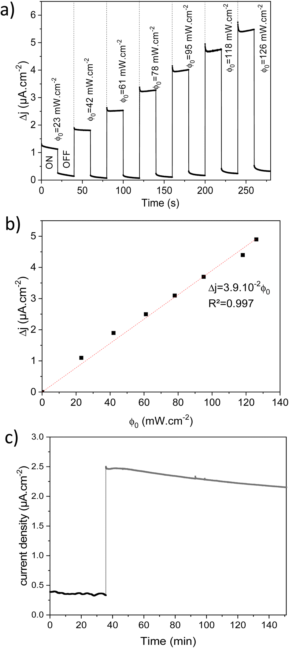 | ||
| Fig. 7 (a) Variation of current density (Δj) under illumination or dark depending on the light intensity (450 nm) and with an applied potential of 0.4 V vs. Ag/AgCl; (b) Δj vs. ϕ0 plot and linear fit in dotted lines; (c) stability test on β-Cu2V2O7 thin film at 0.4 V vs. Ag/AgCl under front-side illumination of 450 nm (61 mW cm−2) and in 0.1 M NaBi buffer solution (pH = 9.2). | ||
Finally, Cu2V2O7 is also known to exhibit photocorrosion phenomenon.8 The stability of the films was thus studied by chronoamperometry in 0.1 M NaBi buffer solution (pH = 9.2) and with a constant applied potential of 0.4 V vs. Ag/AgCl (Fig. 7c). For the β-Cu2V2O7 thin films, one can see that the anode current density is relatively stable, then undergoes a slight decrease with time. This drops to 8% over 1 hour under 450 nm illumination (ϕ0 = 95 mW cm−2). This decrease is mainly due to a gradual dissolution of the photoanode in the electrolyte. Indeed, this deterioration can be induced by the formation of O2 bubbles at the interface and/or a reaction with the electrolyte because the zone of stability (pH) of the oxide is very small.59 This phenomenon has also been observed in the case of Cu2V2O7 films, e.g. I. Khan et al.16 indicate a decrease of 2% and 14% in 1000 s for Cu2V2O7 produced at 500 °C and 250 °C, respectively. In order to check this point, we performed an image of the surface of the Cu2V2O7 thin film and maps for the V, In and Cu elements between a zone not subjected or subjected to the electrolyte. In Fig. 8, we can clearly observe the demarcation zone between a part subjected to the electrolyte showing circular corrosion phenomena and a part corresponding to the initial thin layer having a smooth appearance whose surface is constituted of granular conglomerates. The absence of copper and vanadium in these cracks confirms the corrosion of the film during prolonged use. The effect of the electrolyte on the stability of the film is demonstrated and will require work on the formulation of the electrolyte in order to improve this stability. Nevertheless, the results obtained on the films of β-Cu2V2O7 produced by PLD shows that it can be used for applications as a particularly active photoanode or as photodetector in the blue spectral region. Nevertheless, the photostability needs to be improved in the futures studies. We can consider two paths: (i) improved the chemical stability with respect to the electrolyte or (ii) the encapsulation in order to protect the photoanode. For this last point, this method has already been used successfully to protect hybrid halide perovskite by a double-layer graphite sheet/nickel (GS/Ni).60
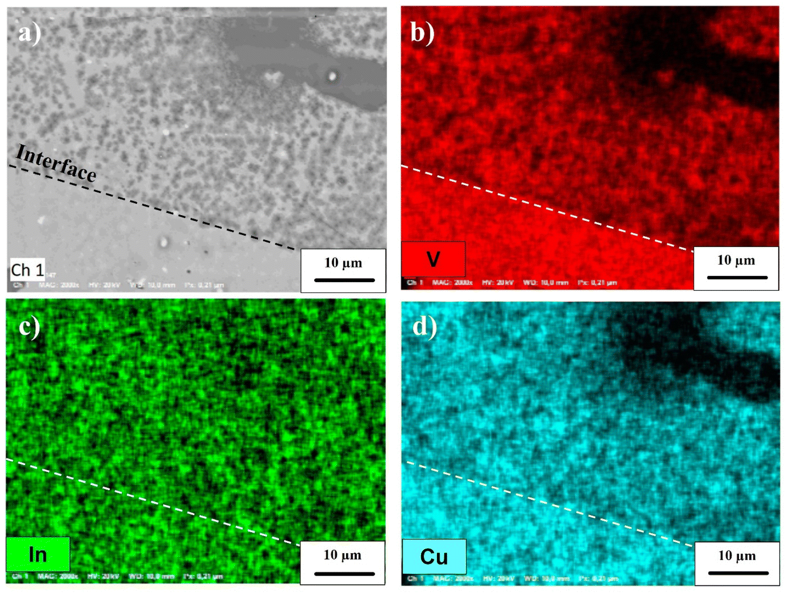 | ||
| Fig. 8 (a) SEM image of Cu2V2O7 thin film after the photocorrosion test (the interface delimits the submerged surface at the top of the image); (b)–(d) colorized elementary maps for vanadium, indium and copper elements, respectively. | ||
4. Conclusion
In this work, two polymorphic forms of copper pyrovanadate (α- and β-Cu2V2O7) were synthesized by solid-state reaction. The study of HT-XRD and TGA/DSC, allowed to determine the mechanisms governing phase transitions within copper vanadate. The evolution of the lattice parameters as a function of temperature has shown a non-linear evolution of the thermal expansion coefficient within the two phases (α-/β-Cu2V2O7). In addition, TGA/DSC analysis also determined the congruent melting temperature of Cu2V2O7, thus obtaining dense ceramics that can be used as a target for the Pulsed Laser Deposition (PLD) technique. The photoelectrochemical properties have been studied both on thick films produced by the drop casting method and on thin films synthesized by PLD on glass/ITO substrates. In the case of thick Cu2V2O7 films, the results showed the generation of a larger photocurrent in the blue spectral region. In addition, the evolution of the variation of the current density between illumination and dark shows a double tendency with a linear growth then evolution in power law. From the transient photocurrent response, the recombination and transfer constants were calculated, showing that ktr is very close to krec. In the case of thin films, the generated photocurrent presents a better efficiency for 450 nm illumination. In addition, the evolution of the variation in current density between illumination and dark shows a linear trend indicating the presence of a significant concentration of traps. However, the transient photocurrent response showed a lower instantaneous spike indicating a higher ktr/krec ratio. Finally, a phenomenon of photocorrosion within thin films representing 8% for one hour was demonstrated in this work.Conflicts of interest
There are no conflicts to declare.Acknowledgements
DIM 1: Energetic efficiency of the UArtois is thanked for its financial support for this project. Chevreul Institute (FR 2638), “Région Nord Pas-de-Calais” and “FEDER” are also acknowledged for supporting and funding this work. The authors would like to thank N. Kanida for its contribution on thermal analyzes. The SEM measurements were accomplished in the Central Laboratories unit at Qatar University. This work was also supported by Qatar University under grant number IRCC-2019-003.References
- V. M. Fthenakis, and P. A. Lynn, Electricity from Sunlight: Photovoltaic-Systems Integration and Sustainability, John Wiley & Sons, 2018, ISBN: 978-1-118-96380-7 Search PubMed.
- J. H. Kim, D. Hansora, P. Sharma, J.-W. Jang and J. S. Lee, Toward practical solar hydrogen production – an artificial photosynthetic leaf-to-farm challenge, Chem. Soc. Rev., 2019, 48, 1908–1971, 10.1039/C8CS00699G.
- N. Jamalullail, I. S. Mohamad, M. N. Norizan, N. Mahmed and B. N. Taib, Recent improvements on TiO2 and ZnO nanostructure photoanode for dye sensitized solar cells: A brief review, EPJ Web Conf., 2017, 162, 01045, DOI:10.1051/epjconf/201716201045.
- N. D. Sankir, and M. Sankir, Photoelectrochemical Solar Cells, John Wiley & Sons, 2018, ISBN:978-1-119-45993-4 Search PubMed.
- S. Irvine, Solar Cells and Photovoltaics, in Springer Handb. Electron. Photonic Mater., ed. S. Kasap, and P. Capper, Springer International Publishing, Cham, 2017, DOI:10.1007/978-3-319-48933-9_43.
- M. Pavan, S. Rühle, A. Ginsburg, D. A. Keller, H.-N. Barad, P. M. Sberna, D. Nunes, R. Martins, A. Y. Anderson, A. Zaban and E. Fortunato, TiO2/Cu2O all-oxide heterojunction solar cells produced by spray pyrolysis, Sol. Energy Mater. Sol. Cells, 2015, 132, 549–556, DOI:10.1016/j.solmat.2014.10.005.
- G. Hodes and P. V. Kamat, Understanding the Implication of Carrier Diffusion Length in Photovoltaic Cells, J. Phys. Chem. Lett., 2015, 6, 4090–4092, DOI:10.1021/acs.jpclett.5b02052.
- N. Guijarro, P. Bornoz, M. Prévot, X. Yu, X. Zhu, M. Johnson, X. Jeanbourquin, F. L. Formal and K. Sivula, Evaluating spinel ferrites MFe2O4 (M = Cu, Mg, Zn) as photoanodes for solar water oxidation: prospects and limitations, Sustainable Energy Fuels, 2017, 2, 103–117, 10.1039/C7SE00448F.
- S. Ida, K. Yamada, T. Matsunaga, H. Hagiwara, Y. Matsumoto and T. Ishihara, Preparation of p-Type CaFe2O4 Photocathodes for Producing Hydrogen from Water, J. Am. Chem. Soc., 2010, 132, 17343–17345, DOI:10.1021/ja106930f.
- M. S. Prévot, N. Guijarro and K. Sivula, Enhancing the Performance of a Robust Sol–Gel-Processed p-Type Delafossite CuFeO2 Photocathode for Solar Water Reduction, ChemSusChem, 2015, 8, 1359–1367, DOI:10.1002/cssc.201403146.
- J. E. Park, Y. Hu, J. W. Krizan, Q. D. Gibson, U. T. Tayvah, A. Selloni, R. J. Cava and A. B. Bocarsly, Stable Hydrogen Evolution from an AgRhO2 Photocathode under Visible Light, Chem. Mater., 2018, 30, 2574–2582, DOI:10.1021/acs.chemmater.7b04911.
- S. N. Tijare, M. V. Joshi, P. S. Padole, P. A. Mangrulkar, S. S. Rayalu and N. K. Labhsetwar, Photocatalytic hydrogen generation through water splitting on nano-crystalline LaFeO3 perovskite, Int. J. Hydrogen Energy, 2012, 37, 10451–10456, DOI:10.1016/j.ijhydene.2012.01.120.
- P. Yilmaz, D. Yeo, H. Chang, L. Loh and S. Dunn, Perovskite BiFeO3 thin film photocathode performance with visible light activity, Nanotechnology, 2016, 27, 345402, DOI:10.1088/0957-4484/27/34/345402.
- M. I. Díez-García and R. Gómez, Progress in Ternary Metal Oxides as Photocathodes for Water Splitting Cells: Optimization Strategies, Sol. RRL, 2022, 6, 2100871, DOI:10.1002/solr.202100871.
- W. Guo, W. D. Chemelewski, O. Mabayoje, P. Xiao, Y. Zhang and C. B. Mullins, Synthesis and Characterization of CuV2O6 and Cu2V2O7: Two Photoanode Candidates for Photoelectrochemical Water Oxidation, J. Phys. Chem. C, 2015, 119, 27220–27227, DOI:10.1021/acs.jpcc.5b07219.
- I. Khan and A. Qurashi, Shape Controlled Synthesis of Copper Vanadate Platelet Nanostructures, Their Optical Band Edges, and Solar-Driven Water Splitting Properties, Sci. Rep., 2017, 7, 1–11, DOI:10.1038/s41598-017-14111-7.
- C. Gadiyar, M. Strach, P. Schouwink, A. Loiudice and R. Buonsanti, Chemical transformations at the nanoscale: nanocrystal-seeded synthesis of β-Cu2V2O7 with enhanced photoconversion efficiencies, Chem. Sci., 2018, 9, 5658–5665, 10.1039/C8SC01314D.
- C.-M. Jiang, M. Farmand, C. H. Wu, Y.-S. Liu, J. Guo, W. S. Drisdell, J. K. Cooper and I. D. Sharp, Electronic Structure, Optoelectronic Properties, and Photoelectrochemical Characteristics of γ-Cu3V2O8, Thin Films, 2017, 29(7), 3334–3345, DOI:10.1021/acs.chemmater.7b00807.
- B. Chattopadhyay, Md. A. Ahmed, S. Bandyopadhyay, R. Singha and P. Mandal, Magnetic ordering induced ferroelectricity in α-Cu2V2O7 studied through non-magnetic Zn doping, J. Appl. Phys., 2017, 121, 094103, DOI:10.1063/1.4977859.
- S. Kalal, A. Pandey, R. Ameta and P. B. Punjabi, Heterogeneous photo-Fenton-like catalysts Cu2V2O7 and Cr2V4O13 for an efficient removal of azo dye in water, Cogent Chem., 2016, 2, 1143344, DOI:10.1080/23312009.2016.1143344.
- M. P. Rao, A. K. Akhila, J. J. Wu, A. M. Asiri and S. Anandan, Synthesis, characterization and adsorption properties of Cu2V2O7 nanoparticles, Solid State Sci., 2019, 92, 13–23, DOI:10.1016/j.solidstatesciences.2019.03.021.
- M. Kim, B. Joshi, H. Yoon, T. Y. Ohm, K. Kim, S. S. Al-Deyab and S. S. Yoon, Electrosprayed copper hexaoxodivanadate (CuV2O6) and pyrovanadate (Cu2V2O7) photoanodes for efficient solar water splitting, J. Alloys Compd., 2017, 708, 444–450, DOI:10.1016/j.jallcom.2017.02.302.
- S. S. Kalanur and H. Seo, Facile growth of compositionally tuned copper vanadate nanostructured thin films for efficient photoelectrochemical water splitting, Appl. Catal., B, 2019, 249, 235–245, DOI:10.1016/j.apcatb.2019.02.069.
- M. Machida, J. Yabunaka and T. Kijima, Efficient photocatalytic decomposition of water with the novel layered tantalate RbNdTa2O7, Chem. Commun., 1999, 19, 1939–1940, 10.1039/A905246A.
- T. Hillel and Y. Ein-Eli, Copper vanadate as promising high voltage cathodes for Li thermal batteries, J. Power Sources, 2013, 229, 112–116, DOI:10.1016/j.jpowsour.2012.11.128.
- Y. Wang, L. Cao, J. Huang, J. Lu, B. Zhang, G. Hai and N. Jia, Enhanced cyclic performance of Cu2V2O7/reduced Graphene Oxide mesoporous microspheres assembled by nanoparticles as anode for Li-ion battery, J. Alloys Compd., 2017, 724, 421–426, DOI:10.1016/j.jallcom.2017.07.070.
- J. Yamaki and A. Yamaji, Layered materials for lithium secondary batteries, Physica B+C, 1981, 105, 466–470, DOI:10.1016/0378-4363(81)90296-5.
- D. Mercurio-Lavaud and B. Frit, Structure cristalline de la variété basse température du pyrovanadate de cuivre: α-Cu2V2O7, Acta Crystallogr., Sect. B: Struct. Crystallogr. Cryst. Chem., 1973, 29, 2737–2741, DOI:10.1107/S0567740873007478.
- J. M. Hughes and R. W. Birnie, Ziesite, β-Cu2V2O7, a new copper vanadate and fumarole temperature indicator, Am. Mineral., 1980, 65(11–12), 1146–1149 CAS.
- S. V. Krivovichev, S. K. Filatov, P. N. Cherepansky, T. Armbruster and O. Y. Pankratova, Crystal structure of γ-Cu2V2O7 and its comparaison to blossite (α-Cu2V2O7) and ziesite (β-Cu2V2O7), Can. Mineral., 2005, 43, 671–677, DOI:10.2113/gscanmin.43.2.671.
- G. M. Clark and R. Garlick, Formation and properties of copper(II) divanadate(V), J. Inorg. Nucl. Chem., 1978, 40, 1347–1349, DOI:10.1016/0022-1902(78)80048-7.
- M. Eguchi, I. Furusawa, T. Miura and T. Kishi, Lithium insertion characteristics of β-Cu2V2O7, Solid State Ionics, 1994, 68, 159–164, DOI:10.1016/0167-2738(94)90253-4.
- M. Sato, V. Warne-Lang, Y. Kadowaki, N. Katayama, Y. Okamoto and K. Takenaka, Sol–gel synthesis of doped Cu2V2O7 fine particles showing giant negative thermal expansion, AIP Adv., 2020, 10, 075207, DOI:10.1063/5.0010631.
- G. Han, S. Yang, Y. Huang, J. Yang, W. Chai, R. Zhang and D. Chen, Hydrothermal synthesis and electrochemical sensing properties of copper vanadate nanocrystals with controlled morphologies, Trans. Nonferrous Met. Soc. China, 2017, 27, 1105–1116, DOI:10.1016/S1003-6326(17)60129-8.
- V. Sivakumar, R. Suresh, K. Giribabu, R. Manigandan, S. Munusamy, S. Praveen Kumar, S. Muthamizh and V. Narayanan, Copper vanadate nanoparticles: synthesis, characterization and its electrochemical sensing property, J. Mater. Sci.: Mater. Electron., 2014, 25, 1485–1491, DOI:10.1007/s10854-014-1757-x.
- Z. He and Y. Ueda, Flux Growth of β-Cu2V2O7 Single Crystals in a Closed Crucible, Cryst. Growth Des., 2008, 8, 2223–2226, DOI:10.1021/cg7007478.
- W. Guo, X. Lian, Y. Nie, M. Hu, L. Wu, H. Gao and T. Wang, Facile growth of β-Cu2V2O7 thin films and characterization for photoelectrochemical water oxidation, Mater. Lett., 2020, 258, 126842, DOI:10.1016/j.matlet.2019.126842.
- L. Zhou, Q. Yan, J. Yu, R. J. R. Jones, N. Becerra-Stasiewicz, S. K. Suram, A. Shinde, D. Guevarra, J. B. Neaton, K. A. Persson and J. M. Gregoire, Stability and self-passivation of copper vanadate photoanodes under chemical, electrochemical, and photoelectrochemical operation, Phys. Chem. Chem. Phys., 2016, 18, 9349–9352, 10.1039/C6CP00473C.
- J. Gao, Polymer Light-Emitting Electrochemical Cells, Lumin. Mater. Appl., 2008, 161–205, DOI:10.1002/9780470985687.ch5.
- L. Lutterotti, S. Matthies and H.-R. Wenk, MAUD: a friendly Java program for material analysis using diffraction, Newsletter of the CPD, 1999, 21(14), 15 Search PubMed.
- D. de Waal and C. Hutter, Vibrational spectra of two phases of copper pyrovanadate and some solid solutions of copper and magnesium pyrovanadate, Mater. Res. Bull., 1994, 29, 843–849, DOI:10.1016/0025-5408(94)90004-3.
- M. Machida, T. Kawada, S. Hebishima, S. Hinokuma and S. Takeshima, Macroporous Supported Cu–V Oxide as a Promising Substitute of the Pt Catalyst for Sulfuric Acid Decomposition in Solar Thermochemical Hydrogen Production, Chem. Mater., 2012, 24, 557–561, DOI:10.1021/cm2031637.
- P. F. Newhouse, D. A. Boyd, A. Shinde, D. Guevarra, L. Zhou, E. Soedarmadji, G. Li, J. B. Neaton and J. M. Gregoire, Solar fuel photoanodes prepared by inkjet printing of copper vanadates, J. Mater. Chem. A, 2016, 4, 7483–7494, 10.1039/C6TA01252C.
- B. V. Slobodin, L. L. Surat and R. F. Samigullina, Polymorphism in copper pyrovanadate, Russ. J. Inorg. Chem., 2009, 54, 797–802, DOI:10.1134/S0036023609050192.
- B. V. Slobodin and R. F. Samigullina, Thermoanalytical study of the polymorphism and melting behavior of Cu2V2O7, Inorg. Mater., 2010, 46, 196–200, DOI:10.1134/S0020168510020196.
- W. Miller, C. W. Smith, D. S. Mackenzie and K. E. Evans, Negative thermal expansion: a review, J. Mater. Sci., 2009, 44, 5441–5451, DOI:10.1007/s10853-009-3692-4.
- N. Zhang, L. Li, M. Wu, Y. Li, D. Feng, C. Liu, Y. Mao, J. Guo, M. Chao and E. Liang, Negative thermal expansion and electrical properties of α-Cu2V2O7, J. Eur. Ceram. Soc., 2016, 36, 2761–2766, DOI:10.1016/j.jeurceramsoc.2016.04.030.
- S. A. Petrova, R. G. Zakharov, M. V. Rotermel’, T. I. Krasnenko and N. A. Vatolin, A new high-temperature modification of copper pyrovanadate, Dokl. Chem., 2005, 400, 30–33, DOI:10.1007/s10631-005-0015-4.
- H. Wang, M. Yang, M. Chao, J. Guo, Q. Gao, Y. Jiao, X. Tang and E. Liang, Negative thermal expansion property of β-Cu2V2O7, Solid State Ionics, 2019, 343, 115086, DOI:10.1016/j.ssi.2019.115086.
- H. T. Yi, P. Irkhin, P. P. Joshi, Y. N. Gartstein, X. Zhu and V. Podzorov, Experimental Demonstration of Correlated Flux Scaling in Photoconductivity and Photoluminescence of Lead-Halide Perovskites, Phys. Rev. Appl., 2018, 10, 054016, DOI:10.1103/PhysRevApplied.10.054016.
- T. S. Moss, Photoconductivity in the elements, Butterworths Scientific Publications, London, 1952 Search PubMed.
- B. Ullrich and H. Xi, Photocurrent limit in nanowires, Opt. Lett., 2013, 38, 4698–4700, DOI:10.1364/OL.38.004698.
- C. Y. Cummings, F. Marken, L. M. Peter, A. A. Tahir and K. G. U. Wijayantha, Kinetics and mechanism of light-driven oxygen evolution at thin film α-Fe2O3 electrodes, Chem. Commun., 2012, 48, 2027–2029, 10.1039/c2cc16382a.
- L. M. Peter, K. G. U. Wijayantha and A. A. Tahir, Kinetics of light-driven oxygen evolution at α-Fe2O3 electrodes, Faraday Discuss., 2012, 155, 309–322, 10.1039/C1FD00079A.
- L. M. Peter, Energetics and kinetics of light-driven oxygen evolution at semiconductor electrodes: the example of hematite, J. Solid State Electrochem., 2013, 17, 315–326, DOI:10.1007/s10008-012-1957-3.
- Basic Theories of Semiconductor Electrochemistry, in Electrochem. Silicon Its Oxide, ed. X. G. Zhang, Springer US, Boston, MA, 2001, pp. 1–43, DOI:10.1007/0-306-47921-4_1.
- K. Gelderman, L. Lee and S. W. Donne, Flat-Band Potential of a Semiconductor: Using the Mott–Schottky Equation, J. Chem. Educ., 2007, 84, 685, DOI:10.1021/ed084p685.
- H. Mortadi, E. Sabbar and M. Bettach, Electrical conductivity and dielectric behavior in copper divanadates, Phys. B, 2019, 561, 159–163, DOI:10.1016/j.physb.2019.03.001.
- L. Zhou, Q. Yan, J. Yu, R. J. R. Jones, N. Becerra-Stasiewicz, S. K. Suram, A. Shinde, D. Guevarra, J. B. Neaton, K. A. Persson and J. M. Gregoire, Stability and self-passivation of copper vanadate photoanodes under chemical, electrochemical, and photoelectrochemical operation, Phys. Chem. Chem. Phys., 2016, 18, 9349–9352, 10.1039/C6CP00473C.
- M. Wang, Y. Li, X. Cui, Q. Zhang, S. Pan, S. Mazumdar, Y. Zhao and X. Zhang, High-Performance and Stable Perovskite-Based Photoanode Encapsulated by Blanket-Cover Method, ACS Appl. Energy Mater., 2021, 4(8), 7526–7534, DOI:10.1021/acsaem.1c00051.
Footnote |
| † Electronic supplementary information (ESI) available. See DOI: https://doi.org/10.1039/d3ra01509b |
| This journal is © The Royal Society of Chemistry 2023 |