
 Open Access Article
 This Open Access Article is licensed under a Creative Commons Attribution-Non Commercial 3.0 Unported Licence
Janus structures of the C2h polymorph of gallium monochalcogenides: first-principles examination of Ga2XY (X/Y = S, Se, Te) monolayers
Tuan-Anh Tran a,
Le S. Haia,
Vo T. T. Vib,
Cuong Q. Nguyencd,
Nguyen T. Nghieme,
Le T. P. Thaof and
Nguyen N. Hieu*cd
a,
Le S. Haia,
Vo T. T. Vib,
Cuong Q. Nguyencd,
Nguyen T. Nghieme,
Le T. P. Thaof and
Nguyen N. Hieu*cd
aFaculty of Applied Sciences, Ho Chi Minh City University of Technology and Education, Ho Chi Minh City, Vietnam
bFaculty of Basic Sciences, University of Medicine and Pharmacy, Hue University, Hue, Vietnam
cInstitute of Research and Development, Duy Tan University, Da Nang, Vietnam. E-mail: nguyenngochieu1@dtu.edu.vn
dFaculty of Natural Sciences, Duy Tan University, Da Nang, Vietnam
eGraduate University of Science and Technology, Vietnam Academy of Science and Technology, Ha Noi, Vietnam
fFaculty of Physics, University of Science and Education, The University of Da Nang, Da Nang, Vietnam
First published on 18th April 2023
Abstract
Group III monochalcogenide compounds can exist in different polymorphs, including the conventional D3h and C2h phases. Since the bulk form of the C2h-group III monochalcogenides has been successfully synthesized [Phys. Rev. B: Condens. Matter Mater. Phys. 73 (2006) 235202], prospects for research on their corresponding monolayers have also been opened. In this study, we design and systematically consider a series of Janus structures formed from the two-dimensional C2h phase of gallium monochalcogenide Ga2XY (X/Y = S, Se, Te) using first-principles simulations. It is demonstrated that the Janus Ga2XY monolayers are structurally stable and energetically favorable. Ga2XY monolayers exhibit high anisotropic mechanical features due to their anisotropic lattice structure. All Janus Ga2XY are indirect semiconductors with energy gap values in the range from 1.93 to 2.67 eV. Due to the asymmetrical structure, we can observe distinct vacuum level differences between the two surfaces of the examined Janus structures. Ga2XY monolayers have high electron mobility and their carrier mobilities are also highly directionally anisotropic. It is worth noting that the Ga2SSe monolayer possesses superior electron mobility, up to 3.22 × 103 cm2 V−1 s−1, making it an excellent candidate for potential applications in nanoelectronics and nanooptoelectronics.
1 Introduction
For nearly two decades, the field of materials science has grown and expanded dramatically. Particularly, the family of two-dimensional (2D) nanomaterials has received extensive attention and research from the scientific community, both theoretically and experimentally. Emerging in the family of two-dimensional materials is a class of group III monochalcogenides MX, which have been experimentally fabricated, such as InSe,1 GaS,2 and GaSe.3 Physical properties of group III monochalcogenide compounds MX (M = Ga, In; X = S, Se, Te) have been systematically studied recently.4–6 It has been shown that this class of materials has outstanding physical properties and diverse applications in the fields of nanooptoelectronics such as nanophotodetectors, field-effect transistors and so on.Recently, the vertical asymmetric structure, namely the Janus structure of 2D nanomaterials, have been experimentally fabricated.7,8 As a result, a series of new Janus structures have been designed and studied extensively.9–12 Notable for this continuum is the Janus configurations based on group III monochalcogenide monolayers.13–15 The Janus group III monochalcogenide compounds M2XY were predicted to be dynamically and thermodynamically stable.16 The M2STe and M2SeTe monolayers are direct bandgap semiconductors,17–19 while the MXs are indirect bandgap ones. It can be realized that the electronic band structure is changed when the structural symmetry of the material is broken. Besides, the oxygenation of Janus monochalcogenides has also been reported in many previous works.9,14,20 These oxidized monolayers were shown to exhibit stability, and the oxygenation caused the semiconductor-to-metal phase transitions in OGaInSe and OGaInTe structures.9 The high electron mobility in GaInXO system makes this Janus potentially applicable in nanoelectronic devices.
It is well-known that the 2D structures can exist in various polymorphs.21,22 The discovery of different crystal phases of material has provided novel characteristics and applications. MoS2 monolayer can exist in the 2H phase as well as in the 1T′ phase.23,24 Also, group III monochalcogenide InSe monolayer can be stable in both D3d phase25 and D3h phase.26 Not only that, the InSe bulk belonging to the C2h point group has been successfully fabricated experimentally.27,28 This discovery prompted scientists to hope for the possibility of synthesizing the corresponding C2h phase of 2D group III monochalcogenide materials. Theoretical studies have predicted the stability of C2h group III monochalcogenide monolayers.29 MX materials with C2h space group are semiconductors with wider direct bandgaps and their carrier mobilities are much higher than that in the conventional D3h phase. C2h-MX has a strong absorption coefficient and anisotropic optical properties, making new phase potential for application in high-performance optoelectronic devices.29
Following this development, we propose a series of Janus Ga2XY monolayers based on C2h-GaX materials by means of density functional theory. We first focus on their structural features and stability. Besides, the electronic characteristics and also carrier mobilities of Ga2XY are calculated systematically. The article is structured as follows. The next section presents the methodology and computational methods used in this study. The main calculated results of the paper are presented in Section III, including crystal structure characteristics and structural stability, electronic properties, and carrier mobility. The conclusion is presented in Section IV.
2 Computational method
All calculations in this study were computed based on density functional theory (DFT) performed by Quantum Espresso code.30 We used the projector augmented wave approximation to investigate the electron–ion interaction.31 The cut-off energy of 50 Ry was selected for a plane-wave basis. The electron exchange and correlation effect were considered by the functional suggested by Perdew, Burke, and Ernzerhof (PBE).32 Further, we also used Heyd–Scuseria–Ernzerhof (HSE06) hybrid functional33 as implemented in the Vienna ab initio simulation code34,35 to correct bandgap of the investigated structures. A k-points grid of (15 × 15 × 1) was chosen for sampling the first Brillouin zone by the Monkhorst–Pack scheme.36 The convergence threshold of energy and force was selected as 10−6 eV and 10−3 eV Å−1, respectively. The weak van der Waals forces between interlayers were treated by the semiempirical DFT-D3 method37 was adopted to describe the weak van der Waals (vdW) interactions between interlayers. A vacuum space of 20 Å was used along the vertical direction to eliminate possible interactions between neighbor slabs. The phonon dispersions were calculated by the density functional perturbation approximation38 as implemented in the PHONOPY software.39 To test the thermodynamic stability of Janus systems, the ab initio molecular dynamics (AIMD) calculation was performed.40 The carrier mobilities in these Janus were determined based on the deformation potential (DP) theory.413 Results and discussion
3.1 Crystal structure and structural stabilities
Fig. 1 presents the optimized crystal structure of Janus Ga2XY monolayer, which is a monoclinic lamella. The Janus Ga2XY, as shown in Fig. 1, can be formed by substituting the top chalcogen atom layer X with another chalcogen atom layer Y in the C2h-GaX monolayer. The unit cell of Ga2XY contains eight atoms and its crystal structure belongs to the symmetry group Pm (Cs). This is different from the C3v-Ga2XY monolayer (formed from D3h-GaX), where the unit cell contains only four atoms.42 The structural parameters for optimized crystals of Ga2XY monolayers are presented in Table 1. We can see that Janus Ga2XY is a high anisotropic structure with the anisotropic ratio τ = a/b (a and b are the lattice constants) up to about 2.6. The lattice constants increase with the increasing atomic size of the chalcogen atoms X and Y. The lattice constant value a/b ranges from 9.77/3.70 Å (Ga2SSe) to 9.90/3.94 Å (Ga2SeTe). It is demonstrated that the lattice parameter b of Ga2SSe is between that of GaS and GaSe,29 while the lattice constant a of Ga2SSe is smaller than that of both GaS and GaSe.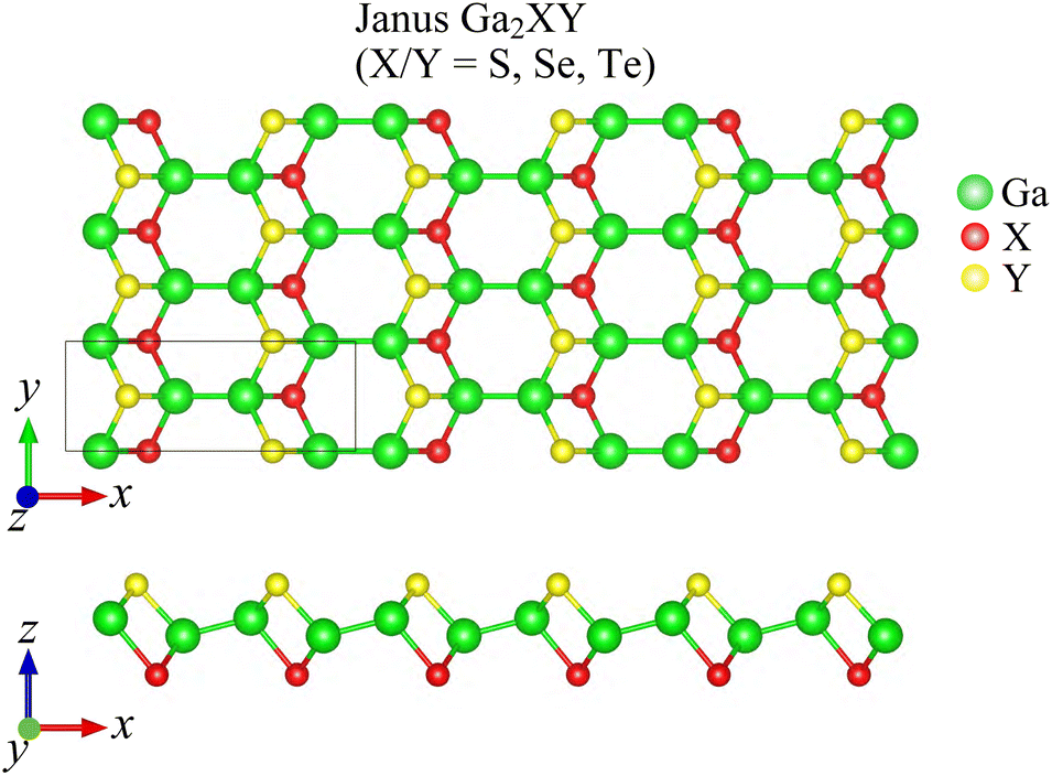 | ||
| Fig. 1 Top and side views of crystal structure of Janus Ga2XY structure (X/Y = S, Se, Te). | ||
| a (Å) | b (Å) | Δh (Å) | τ | Ecoh (eV per atom) | C11 (N m−1) | C12 (N m−1) | C22 (N m−1) | C66 (N m−1) | |
|---|---|---|---|---|---|---|---|---|---|
| Ga2SSe | 9.77 | 3.70 | 3.12 | 2.64 | −4.01 | 40.50 | 2.58 | 47.47 | 9.24 |
| Ga2STe | 9.82 | 3.87 | 3.30 | 2.54 | −3.79 | 32.76 | 3.01 | 43.40 | 6.83 |
| Ga2SeTe | 9.90 | 3.94 | 3.43 | 2.51 | −3.63 | 29.01 | 2.56 | 43.05 | 5.64 |
We next test the structural stabilities of the investigated materials. Firstly, we evaluate the strength of the chemical bonding between atoms in Janus Ga2XY monolayers through the calculations for cohesive energy Ecoh by the following:
 | (1) |
In Table 1, we present the calculated values of the cohesive energies of the Ga2XY monolayers. The cohesive energies of Ga2SSe, Ga2STe and Ga2SeTe are calculated to be −4.01, −3.79 and −3.63 eV per atom, respectively. This suggests that all investigated monolayers are energetically favorable. The greater the distance between the atoms, the weaker the bond between them. Ga2SSe is found to be the most energetically favorable with Ecoh = −4.01 eV per atom. The obtained results for the cohesive energies of Ga2XY are comparable with those of their pristine structures, such as C2h-GaS 4.11 eV per atom and C2h-GaSe 3.75 eV per atom,29 and C3v-Ga2XY Janus structures, such as C3v-Ga2SSe 3.40 eV per atom and C3v-Ga2STe 3.17 eV per atom.43
To determine the realization of Ga2XY monolayers, we evaluate their dynamical stability of the studied monolayers based on the calculations for phonon spectra as shown in Fig. 2(a). It is found that the phonon spectrum of Ga2XY have 24 phonon modes due to its unit cell containing eight atoms, including three acoustic and 21 optical modes. Our calculated results indicate that there are no soft modes (negative frequencies) available in the phonon spectra of all three examined monolayers. This implies that Ga2XY materials are dynamically stable. Further, we also test the thermodynamical stability at room temperature. The AIMD calculations are carried out at 300 K with 5 ps in increments of 1 fs. The variation of the total energy to time for these Janus monolayers is depicted in Fig. 2(b). We found that the fluctuations in the total energy of three proposed Janus structures are small during the AIMD calculations, about 0.5 eV. The crystal structure of the monolayers remains stable. No chemical bond breaks nor structural transition was observed. This proves the thermodynamical stability of the Janus Ga2XY.
 | ||
| Fig. 2 (a) Phonon spectra and (b) AIMD calculation for the variations of the total energy to time of Janus Ga2XY at room temperature. | ||
Besides the thermodynamic stability, we also test the mechanical stability of these new systems through the evaluation of their elastic constants. According to Voigt's notation, we can use four elastic constants C11, C22, C12, and C66 to evaluate the mechanical stability of 2D materials. To determine these elastic constants, we apply the small tension and compression along the two x and y directions. The strain strength varies from −0.015 to 0.015 with a strain step of 0.005. At each strain value, the atomic positions are optimized and the corresponding energy data is obtained. We fit these energy values to a polynomial, thereby attaining the elastic constants Cij.44 Table 2 outlines all the values of the elastic constants of our proposed Janus systems. It is noteworthy that the elastic constants satisfy Born-Huang's criteria for mechanical stability, i.e. C11 > 0 and C112 – C122 > 0,45 revealing that the Janus Ga2XY are found to be mechanically stable.
| EPBEg (eV) | EHSE06g (eV) | ΔΦ (eV) | Φ1 (eV) | Φ2 (eV) | |
|---|---|---|---|---|---|
| Ga2SSe | 1.88 | 2.67 | 0.15 | 5.34 | 5.49 |
| Ga2STe | 1.41 | 2.15 | 0.38 | 5.44 | 5.06 |
| Ga2SeTe | 1.27 | 1.96 | 0.23 | 5.21 | 4.98 |
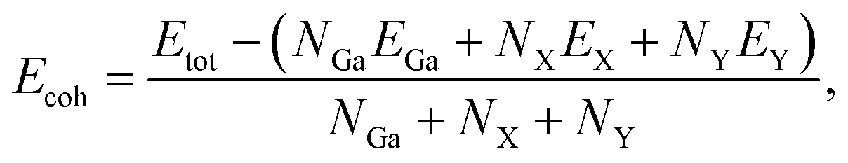
The mechanical properties of materials are also characterized by Young's modulus Y2D and Poisson's ratio  . Young's modulus gives the in-plane strength of a material. Due to the anisotropic crystal structure, Young's modulus of Ga2XY depends on the investigated direction as follows46,47
 | (2) |
Our calculated results present that Young's modulus is high directionally anisotropic due to the in-plane anisotropic lattice of Ga2XY systems. The calculated results for Young's modulus, as shown in Fig. 3(a), indicate that Ga2XY materials are the hardest along the [010] direction (θ = 90°) with Young's modulus of Ga2SSe, Ga2STe, and Ga2SeTe being 47.31, 43.12, and 42.82 N m−1, respectively. Young's modulus along the [100] direction (θ = 0°) is also high while the minimum value is corresponding to θ about 45° and 135°. Fig. 3 reveals that the Ga2SSe has the largest Young's modulus in comparison with other structures. The calculated values of Young's modulus decrease with increasing atomic number of chalcogen elements. This is consistent with the fact that the larger the lattice constant, the weaker the in-plane strength. In general, Ga2XY materials are more mechanically flexible than other compounds because they have a small Young's coefficient.48
 | ||
| Fig. 3 Young's modulus (a) and Poisson's ratio (b) of Ga2XY (X/Y = S, Se, Te). | ||
We also calculate Poisson's ratio  which can determine the mechanical response of the Ga2XY to the applied strain as:46,47
 | (3) |
From Fig. 3(b), it is revealed that the Poisson's ratio of Ga2XY is anisotropic, which is consistent with their in-plane anisotropic lattice. The Janus Ga2SSe has the smallest  value compared with other considered structures. Thus, Poisson's ratio exhibits an opposite trend with respect to Young's modulus. It can be found that the
  value of Ga2XY is much smaller than that of graphene and silicene.48 In other words, the investigated Janus monolayers are very insensitive to applied strain.
3.2 Electronic properties
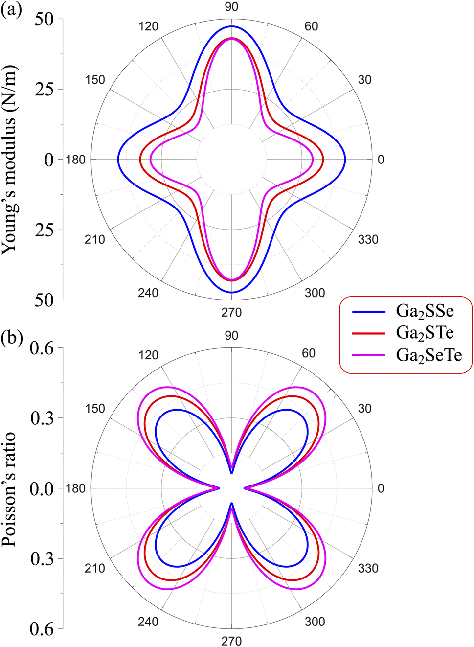
In this section, we focus on the electronic properties of Janus Ga2XY based on the DFT analysis. First, we study the band structures of these Janus structures using both PBE and HSE06 functionals. Fig. 4 reveals that all examined Janus materials are semiconductors. At the PBE level, the calculated bandgaps of Ga2SSe, Ga2STe, and Ga2SeTe are found to be 1.88, 1.41, and 1.27 eV, respectively. It is found that all three investigated structures exhibit indirect semiconducting characteristics. However, while both Ga2STe and Ga2SeTe monolayer have the conduction band minimum (CBM) located at the X point and the valence band maximum located on the YΓ path, the CBM of Ga2SSe located at the Γ point. However, it is worth noting that the difference in energy at the CBM and X point in Ga2SSe is very small. These characteristics of Janus Ga2XY in this phase are different from those in the C3v one, where both C3v-Ga2STe and C3v-Ga2SeTe possess direct band gaps.17,19 It is evident that the variation in the crystal lattice has given rise to new electronic features. | ||
| Fig. 4 Examined energy band diagrams of (a) Ga2SSe, (b) Ga2STe, and (a) Ga2SeTe monolayers using the PBE and HSE06 functionals. | ||
To correct the bandgaps of Ga2XY monolayers, we also calculate the band diagrams by using the hybrid functional HSE06 as depicted in Fig. 4(b). The hybrid functional is considered to be the most efficient method to obtain the precise bandgap of semiconductors and insulators. It can be observed that all Janus monolayers retain the bandgap nature at the PBE level. However, the bandgaps calculated by the HSE06 method is much higher than those by the PBE method as tabulated in Table 2. At the HSE06 level, the bandgaps of Ga2XY semiconductors vary from 1.96 to 2.67 eV. The bandgaps of these structures are comparable with that of C3v-Ga2XY structures.16
To further understand the nature of the electronic structure, we explore the weighted bands of Janus Ga2XY as revealed in Fig. 5. It is obvious that all three Janus Ga2XY monolayers exhibit the same trend in the contributions of the atomic orbitals to the electronic bands. The main component of the conduction band is the s orbital of the Ga atom, while the major contribution of the valence band is the p orbital of the chalcogen atom.
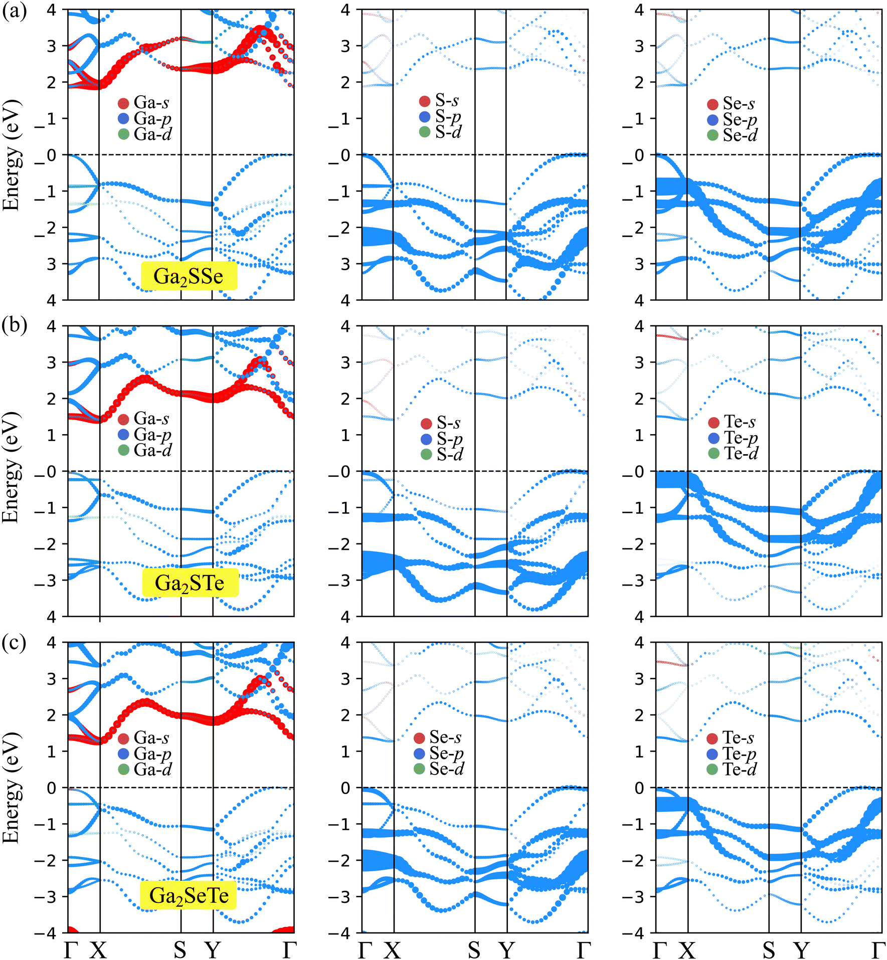 | ||
| Fig. 5 Projected band structures of (a) Ga2SSe, (b) Ga2STe, and (a) Ga2SeTe. | ||
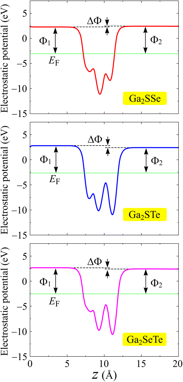
One of the important features of electronic materials is the work function, which represents the ability of electrons to escape from the surface of a material. Possessing the vertical asymmetric lattice, Janus structures possess intrinsic electric fields.49 The magnitude of this electric field depends on the electronegativity difference of the X and Y sides. For the asymmetric structures, we included the dipole correction50 in the calculations of the electrostatic potentials. Fig. 6 depicts the computed the electrostatic potential with dipole correction. We can see that a distinct vacuum level difference ΔΦ is found at the surfaces of Janus Ga2XY. The larger the atomic size difference between X and Y constituent elements, the higher value of ΔΦ is. From Table 2, we can see that, for example, the values of ΔΦ for Ga2SSe and Ga2STe are 0.15 and 0.38 eV, respectively. The value of ΔΦ not only affects the work functions on the surfaces of the materials but also affects the photocatalytic performances of the 2D materials. The value of the work function is determined based on the difference between the Fermi level and the vacuum level. The X and Y surfaces of Janus have different vacuum levels, leading to a disparity in the work functions at the two surfaces. The obtained work functions on both surfaces of Ga2XY are summarized in Table 2. It is demonstrated that the values of the work function on the X side are in the range from 5.21 to 5.44 eV, while those on the Y side are in the range from 4.98 to 5.49 eV. Furthermore, Janus Ga2SeTe has the smallest work function at the two surfaces compared with the other Ga2XY structures. This means that it is easier for the electron escaping from the surfaces of Ga2SeTe compound than for the other structures.
 | ||
| Fig. 6 Calculated electrostatic potentials with dipole corrections of Ga2XY monolayers. | ||
3.3 Carrier mobilities
Mobility of carriers is one of the key parameters affecting the applicability of the material to electronics and optoelectronics. We here examine the carrier mobility of three studied Janus compounds through the deformation potential (DP) theory suggested by Bardeen and Shockley.41 The carrier mobility of a 2D crystal is defined as follows:
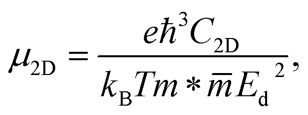 | (4) |
![[m with combining macron]](https://www.rsc.org/images/entities/i_char_006d_0304.gif) denotes the average effective mass
denotes the average effective mass  . T is the temperature set to be 300 K, Ed is the DP constant, and C2D is the elastic modulus. The DP constant derives from
 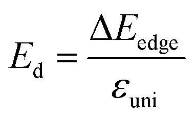 , where ΔEedge is the displacement of the CBM (for electrons) and VBM (for holes) caused by the uniaxial strain εuni. The displacement of these band edges is determined with respect to the vacuum level. By linearly fitting the energy shift of the CBM and VBM as a function of the uniaxial strains as shown in Fig. 7, we obtain the DP constant. The elastic modulus C2D is determined by
  , where E is the total energy of the system, S is the area of the supercell at equilibrium. The carrier effective mass is determined by
  . The effective masses of carriers can be calculated by the parabolic fitting of the values of energies around the CBM and VBM.
 | ||
| Fig. 7 Uniaxial strain-dependence of the total energies (a) and band-edge energies (b) of Ga2XY. The data fitting is represented by the solid line. | ||
Table 3 reports the data of the carrier effective mass, elastic modulus, and DP constant of Ga2XY monolayers along the x and y directions. Based on these obtained parameters, the carrier mobilities in all of Janus are attained accordingly. It is found that the electron and hole mobilities are different in the x and y transport directions, indicating that the carrier mobilities are directionally anisotropic. Particularly, the carrier mobility of Ga2SSe exhibits high anisotropic, where the mobility of electrons along the x direction is much higher than that along the y direction. Ga2SSe monolayer possesses high electron mobility along the x direction up to μx = 3.22 × 103 cm2 V−1 s−1. Similarly, the μx values of Ga2STe and Ga2SeTe are found respectively to be 485.69 and 459.09 cm2 V−1 s−1, which are much higher than their electron mobilities along the y direction μy as presented in Table 3. The carrier mobilities of Ga2STe and Ga2SeTe are comparable to those of the C2h-GaS, C2h-GaSe while Janus Ga2SSe monolayer possesses superior electron mobility compared to that of the pristine C2h-GaX structures.29 However, the electron carrier of Janus Ga2SSe is one order of magnitude smaller than that of the Janus C3v-Ga2SSe (1.31 × 104 cm2 V−1 s−1).51
|
|
C2Dx | C2Dy | E2Dx | C2Dy | μx | μy | ||
|---|---|---|---|---|---|---|---|---|---|
| Ga2SSe | Electron | 0.99 | 0.24 | 57.20 | 65.40 | −0.89 | −12.31 | 3.22 × 10³ | 78.47 |
| Hole | 8.60 | 1.80 | 57.20 | 65.40 | −4.34 | −2.74 | 1.91 | 26.26 | |
| Ga2STe | Electron | 0.86 | 0.23 | 55.00 | 62.10 | −2.52 | −10.01 | 485.69 | 130.57 |
| Hole | 2.35 | 1.26 | 55.00 | 62.10 | −3.67 | −3.64 | 21.48 | 45.98 | |
| Ga2SeTe | Electron | 0.68 | 0.39 | 48.40 | 60.5 | −2.54 | −9.88 | 459.09 | 66.01 |
| Hole | 1.56 | 1.06 | 48.40 | 60.5 | −3.34 | −3.63 | 46.09 | 71.89 |

4 Conclusion
The structural stability, electronic characteristics, and carrier mobilities of Janus materials based on the C2h phase of group III monochalcogenide Ga2XY were investigated using first-principles calculations. Through AIDM calculations and Born-Huang's criteria, all three Janus Ga2XY monolayers are confirmed to be structural stability. The obtained results indicated that Ga2XY monolayers exhibit anisotropic mechanical properties and Ga2XY monolayers are more mechanically flexible than graphene and silicene. Ga2XY monolayers were found to be semiconductors with indirect bandgaps from 1.96 to 2.67 eV at the HSE06 level. With the vertical asymmetric lattice, the distinct vacuum level difference ΔΦ was observed at the surfaces of Janus Ga2XY and the values of ΔΦ depend highly on the atomic size of the constituent atoms X and Y. The obtained results demonstrated that Ga2XY materials exhibit high directional anisotropy. Particularly, the electron mobility of Ga2SSe was found up to 3.22 × 103 cm2 V−1 s−1, which is potential for applications in nanoelectronic devices.Conflicts of interest
There are no conflicts of interest to declare.Acknowledgements
This work belongs to the project grant No: T2022-23 funded by Ho Chi Minh City University of Technology and Education (Vietnam).References
- W. Feng, X. Zhou, W. Q. Tian, W. Zheng and P. Hu, Phys. Chem. Chem. Phys., 2015, 17, 3653 RSC.
- A. Harvey, C. Backes, Z. Gholamvand, D. Hanlon, D. McAteer, H. C. Nerl, E. McGuire, A. Seral-Ascaso, Q. M. Ramasse, N. McEvoy, S. Winters, N. C. Berner, D. McCloskey, J. F. Donegan, G. S. Duesberg, V. Nicolosi and J. N. Coleman, Chem. Mater., 2015, 27, 3483 CrossRef CAS.
- P. Hu, Z. Wen, L. Wang, P. Tan and K. Xiao, ACS Nano, 2012, 6, 5988 CrossRef CAS PubMed.
- S. Demirci, N. Avazli, E. Durgun and S. Cahangirov, Phys. Rev. B, 2017, 95, 115409 CrossRef.
- V. T. Vi, N. N. Hieu, B. D. Hoi, N. T. Binh and T. V. Vu, Superlattices Microstruct., 2020, 140, 106435 CrossRef CAS.
- A. V. Lugovskoi, M. I. Katsnelson and A. N. Rudenko, Phys. Rev. Lett., 2019, 123, 176401 CrossRef CAS PubMed.
- A.-Y. Lu, H. Zhu, J. Xiao, C.-P. Chuu, Y. Han, M.-H. Chiu, C.-C. Cheng, C.-W. Yang, K.-H. Wei, Y. Yang, Y. Wang, D. Sokaras, D. Nordlund, P. Yang, D. A. Muller, M.-Y. Chou, X. Zhang and L.-J. Li, Nat. Nanotechnol., 2017, 12, 744 CrossRef CAS PubMed.
- J. Zhang, S. Jia, I. Kholmanov, L. Dong, D. Er, W. Chen, H. Guo, Z. Jin, V. B. Shenoy, L. Shi and J. Lou, ACS Nano, 2017, 11, 8192–8198 CrossRef CAS PubMed.
- T. V. Vu, V. T. T. Vi, H. V. Phuc, A. I. Kartamyshev and N. N. Hieu, Phys. Rev. B, 2021, 104, 115410 CrossRef CAS.
- F. Li, W. Wei, P. Zhao, B. Huang and Y. Dai, J. Phys. Chem. Lett., 2017, 8, 5959–5965 CrossRef CAS PubMed.
- L. Dong, J. Lou and V. B. Shenoy, ACS Nano, 2017, 11, 8242–8248 CrossRef CAS PubMed.
- A. Mogulkoc, Y. Mogulkoc, S. Jahangirov and E. Durgun, J. Phys. Chem. C, 2019, 123, 29922–29931 CrossRef CAS.
- N. N. Hieu, H. V. Phuc, A. I. Kartamyshev and T. V. Vu, Phys. Rev. B, 2022, 105, 075402 CrossRef CAS.
- T. V. Vu, C. V. Nguyen, H. V. Phuc, A. A. Lavrentyev, O. Y. Khyzhun, N. V. Hieu, M. M. Obeid, D. P. Rai, H. D. Tong and N. N. Hieu, Phys. Rev. B, 2021, 103, 085422 CrossRef CAS.
- H. T. T. Nguyen, V. T. T. Vi, T. V. Vu, N. V. Hieu, D. V. Lu, D. P. Rai and N. T. T. Binh, RSC Adv., 2020, 10, 44785–44792 RSC.
- A. Huang, W. Shi and Z. Wang, J. Phys. Chem. C, 2019, 123, 11388 CrossRef CAS.
- T. V. Vu, V. T. T. Vi, C. V. Nguyen, H. V. Phuc and N. N. Hieu, J. Phys. D: Appl. Phys., 2020, 53, 455302 CrossRef CAS.
- T. V. Vu, V. T. T. Vi, H. V. Phuc, C. V. Nguyen, N. A. Poklonski, C. A. Duque, D. P. Rai, B. D. Hoi and N. N. Hieu, J. Phys.: Condens. Matter, 2021, 33, 225503 CrossRef CAS PubMed.
- H. T. Nguyen, V. T. Vi, T. V. Vu, H. V. Phuc, C. V. Nguyen, H. D. Tong, L. T. Hoa and N. N. Hieu, Phys. E, 2020, 124, 114358 CrossRef CAS.
- M. Demirtas, B. Ozdemir, Y. Mogulkoc and E. Durgun, Phys. Rev. B, 2020, 101, 075423 CrossRef CAS.
- J. L. Zhang, S. Zhao, C. Han, Z. Wang, S. Zhong, S. Sun, R. Guo, X. Zhou, C. D. Gu, K. D. Yuan, Z. Li and W. Chen, Nano Lett., 2016, 16, 4903–4908 CrossRef CAS PubMed.
- S. Y. Lim, J.-U. Lee, J. H. Kim, L. Liang, X. Kong, T. T. H. Nguyen, Z. Lee, S. Cho and H. Cheong, Nanoscale, 2020, 12, 8563–8573 RSC.
- S. Shi, Z. Sun and Y. H. Hu, J. Mater. Chem. A, 2018, 6, 23932–23977 RSC.
- X. Li and H. Zhu, J. Materiomics, 2015, 1, 33–44 CrossRef.
- Y. Sun, Y. Li, T. Li, K. Biswas, A. Patanè and L. Zhang, Adv. Funct. Mater., 2020, 30, 2001920 CrossRef CAS PubMed.
- D. A. Bandurin, A. V. Tyurnina, G. L. Yu, A. Mishchenko, V. Zólyomi, S. V. Morozov, R. K. Kumar, R. V. Gorbachev, Z. R. Kudrynskyi, S. Pezzini, Z. D. Kovalyuk, U. Zeitler, K. S. Novoselov, A. Patanè, L. Eaves, I. V. Grigorieva, V. I. Fal’ko, A. K. Geim and Y. Cao, Nat. Nanotechnol., 2017, 12, 223–227 CrossRef CAS PubMed.
- D. Errandonea, D. Martínez-García, A. Segura, A. Chevy, G. Tobias, E. Canadell and P. Ordejon, Phys. Rev. B: Condens. Matter Mater. Phys., 2006, 73, 235202 CrossRef.
- L. Ghalouci, F. Taibi, F. Ghalouci and M. Bensaid, Comput. Mater. Sci., 2016, 124, 62–77 CrossRef CAS.
- T. Hu, C. Xu, A. Zhang and P. Yu, Mater. Adv., 2022, 3, 2213–2221 RSC.
- P. Giannozzi, S. Baroni, N. Bonini, M. Calandra, R. Car, C. Cavazzoni, D. Ceresoli, G. L. Chiarotti, M. Cococcioni, I. Dabo, A. D. Corso, S. de Gironcoli, S. Fabris, G. Fratesi, R. Gebauer, U. Gerstmann, C. Gougoussis, A. Kokalj, M. Lazzeri, L. Martin-Samos, N. Marzari, F. Mauri, R. Mazzarello, S. Paolini, A. Pasquarello, L. Paulatto, C. Sbraccia, S. Scandolo, G. Sclauzero, A. P. Seitsonen, A. Smogunov, P. Umari and R. M. Wentzcovitch, J. Phys.: Condens. Matter, 2009, 21, 395502 CrossRef PubMed.
- P. E. Blöchl, Phys. Rev. B: Condens. Matter Mater. Phys., 1994, 50, 17953 CrossRef PubMed.
- J. P. Perdew, K. Burke and M. Ernzerhof, Phys. Rev. Lett., 1996, 77, 3865 CrossRef CAS PubMed.
- J. Heyd, G. E. Scuseria and M. Ernzerhof, J. Chem. Phys., 2003, 118, 8207 CrossRef CAS.
- G. Kresse and J. Furthmüller, Phys. Rev. B: Condens. Matter Mater. Phys., 1996, 54, 11169–11186 CrossRef CAS PubMed.
- G. Kresse and J. Furthmüller, Comput. Mater. Sci., 1996, 6, 15–50 CrossRef CAS.
- J. D. Pack and H. J. Monkhorst, Phys. Rev. B: Solid State, 1977, 16, 1748–1749 CrossRef.
- S. Grimme, J. Antony, S. Ehrlich and H. Krieg, J. Chem. Phys., 2010, 132, 154104 CrossRef PubMed.
- T. Sohier, M. Calandra and F. Mauri, Phys. Rev. B, 2017, 96, 075448 CrossRef.
- A. Togo, L. Chaput and I. Tanaka, Phys. Rev. B: Condens. Matter Mater. Phys., 2015, 91, 094306 CrossRef.
- S. Nosé, J. Chem. Phys., 1984, 81, 511 CrossRef.
- J. Bardeen and W. Shockley, Phys. Rev., 1950, 80, 72 CrossRef CAS.
- T. V. Vu, V. T. T. Vi, C. V. Nguyen, H. V. Phuc and N. N. Hieu, J. Phys. D: Appl. Phys., 2020, 53, 455302 CrossRef CAS.
- Y. Bai, Q. Zhang, N. Xu, K. Deng and E. Kan, Appl. Surf. Sci., 2019, 478, 522–531 CrossRef CAS.
- K.-A. N. Duerloo, M. T. Ong and E. J. Reed, J. Phys. Chem. Lett., 2012, 3, 2871–2876 CrossRef CAS.
- M. Born and K. Huang, Am. J. Phys., 1955, 23, 474 CrossRef.
- N. T. Hung, A. R. T. Nugraha and R. Saito, J. Phys. D: Appl. Phys., 2018, 51, 075306 CrossRef.
- P. Xiang, S. Sharma, Z. M. Wang, J. Wu and U. Schwingenschlögl, ACS Appl. Mater. Interfaces, 2020, 12, 30731 CrossRef CAS PubMed.
- H. Şahin, S. Cahangirov, M. Topsakal, E. Bekaroglu, E. Akturk, R. T. Senger and S. Ciraci, Phys. Rev. B: Condens. Matter Mater. Phys., 2009, 80, 155453 CrossRef.
- C.-F. Fu, J. Sun, Q. Luo, X. Li, W. Hu and J. Yang, Nano Lett., 2018, 18, 6312–6317 CrossRef CAS PubMed.
- L. Bengtsson, Phys. Rev. B: Condens. Matter Mater. Phys., 1999, 59, 12301 CrossRef CAS.
- B. Sa, X. Shen, S. Cai, Z. Cui, R. Xiong, C. Xu, C. Wen and B. Wu, Phys. Chem. Chem. Phys., 2022, 24, 15376–15388 RSC.
| This journal is © The Royal Society of Chemistry 2023 |