DOI:
10.1039/D3RA01199B
(Paper)
RSC Adv., 2023,
13, 13564-13574
Synthesis and characterization of nanostructured graphene-doped selenium
Received
22nd February 2023
, Accepted 18th April 2023
First published on 3rd May 2023
Abstract
In this work, we explore various properties of elemental selenium glass (g-Se) by doping with graphene through the facile melt-quench technique. The structural information of the synthesized sample was found by X-ray diffraction (XRD), X-ray photoelectron spectroscopy (XPS), scanning electron microscopy (SEM), and Raman spectroscopy. The analyses confirm that the graphene-doped g-Se behaves like a glass-ceramic material. Electrical and dielectric measurements were performed to discover the consequences of graphene incorporation on the nano-structure of g-Se. The electrical measurements of the dielectric parameters (i.e., dielectric constant ε′ and loss ε′′) and conductivity (σac) reveal that graphene incorporation causes a rise in the dielectric constant but simultaneously increases dielectric loss. The enhancement in ε′ and ε′′ values is thought to be a consequence of the interface effect between graphene and the host selenium glass. Calorimetric experiments were performed in a standard differential scanning calorimetry (DSC) unit on the glassy nanocomposite in non-isothermal mode. By measuring the kinetic temperatures at four heating rates, the kinetics of the crystallization/glass transition were studied. The results were examined to understand the role of graphene doping on the well-known phase transitions (i.e., glass transition and crystallization) of g-Se.
1. Introduction
The integration of chalcogen elements with graphene facilitates the development of new materials (e.g., alloys, composites, and compounds) that open a gateway to fulfil the growing necessities of global energy storage.1–3 In recent years, an incredible response from researchers has been received by composites of graphene and chalcogenides. The reason behind such huge attention towards these composites is their exceptional electronic characteristics4,5 and their promising possible applications in the areas of energy conversion and storage devices.1–3,6 The use of carbon-based nanomaterials with selenium has become a continuing topic in nanoscience research7,8 because of the promising role of selenium in the fabrication of cathodes in the unique class of sodium/lithium rechargeable batteries.8,9
Various research groups have investigated the properties of mixed selenium and graphene/reduced graphene oxide (RGO) under different conditions.10–18 Peng et al.11 reported wrapping selenium nanoparticles (Se NPs) in reduced graphene oxide. They used a self-assembly approach to achieve RGO encapsulated Se NPs for use as a potential cathode in Li–Se batteries with high power and energy. Youn and co-workers12 developed micro-balls of a fusion of graphene–selenium and investigated their direct utilization as the cathode in secondary batteries of Li–Se. The defect chemistry of Se-doped graphene (SeG) was thoroughly studied by Meng et al.13 This group also determined the number and density of defect states in SeG and found that the catalytic action of SeG is higher than that of pure graphene. Consequently, when Se is doped in graphene, the ionization energy is reduced. This causes the transfer of electrons at the boundary of the electrolyte and electrode. Due to this feature, SeG has become useful for developing dye-sensitized solar cells. Yang et al.14 developed unique quantum dots by doping selenium in graphene and found that these quantum dots perform reversible fluorescent switching. Some groups15,16 established a three-dimensional (3D) hierarchical design of a free-standing cathode using mesoporous carbon/graphene15 and sandwiched an assembly of carbon nanotubes/selenium between graphene nanosheets16 to develop Li–Se batteries with high capacity and durability. Other groups17,18 used a different approach with the same aim by designing a binder-free cathode made of graphene oxide-protected 3D selenium17 and a sandwiched assembly of carbon nanotubes/selenium between graphene nanosheets.18
Selenium is a promising cathode material that has fascinated researchers in the last decade because its volumetric capacity is equivalent to that of the extensively considered sulfur cathode. Another reason is its electrical conductivity, which is considerably higher than that of sulfur. From the above literature survey,10–18 we see that the integration of selenium and graphene may fulfil the requirements of high capacity and durability in rechargeable batteries. Several papers from the last decade use carbon and selenium as the key elements for providing better energy storage solutions.19–45
Most of the derivatives of carbon used for this purpose are carbon bubbles,20 porous carbon nanospheres,21 nanofibers26 and aerogels,22 microporous and mesoporous carbon24,25,32,38 and carbide-derived carbon,30 multi-walled carbon nanotubes.28 Only a few reports are available in which graphene is used10–18 with selenium. Moreover, crystalline selenium is used in such studies10–18 as a dopant while graphene is the host material. Keeping in mind these experimental facts and findings, we selected glassy selenium (g-Se) as the base material and decided to study the outcomes of graphene doping in g-Se. To the best of our knowledge, our present studies are the first attempt to report fundamental studies on the various physical properties of graphene-doped glassy selenium composite (g-Se:Gr). These results form the basis for further advanced studies in the direction of employing g-Se with graphene as a dopant to develop energy storage solutions.
2. Experimental
The proper amounts of 5N pure Se element (Sigma Aldrich, USA) and graphene powder (100 nm) were weighed using an electronic balance with a sensitivity of 0.1 milligram for the synthesis of two samples: (i) pure glassy selenium (g-Se) and (ii) a glassy nanocomposite of Se doped with 1 percent weight of graphene (i.e., g-Se:Gr). The materials were sealed using a high vacuum pump unit to achieve a vacuum of 1 micro-torr inside the quartz tubes. The sealed samples were heated to 950 °C in a muffle furnace for 12 hours. During this period, rocking of each sample was performed to homogenize the samples. The red-hot molten samples were dropped rapidly into chilled water and, by breaking the quartz tubes, bulk samples were obtained. The synthesized samples were investigated using various experimental techniques to perceive the surface morphology and chemical composition. A digital LCR meter (Wayne Kerr Electronics, UK, model 43100) was used to measure the capacitance and dissipation factor and, in parallel plate capacitor configuration, to investigate the temperature and AC frequency-dependent electrical properties. The thermal properties of each sample were investigated using a DSC thermal analyzer (TA Instruments, USA; model Auto Q20) with a heating rate of 10 °C min−1 in a nitrogen atmosphere.
3. Results and discussion
Trigonal selenium (t-Se) is the most thermodynamically stable phase, in which Se atoms are covalently bonded and arranged in infinite chains, forming an anisotropic crystal mess. The existence of this phase in the present sample is established using X-ray powder diffraction, which is the most convenient and effective approach to investigate the crystal structure and crystalline phase of the as-prepared nanocomposite system. The XRD pattern of the as-prepared g-Se:Gr is shown in Fig. 1. The XRDs of g-Se and g-Se:Gr nanocomposite show the two most intense peaks of crystalline t-Se (COD-9008579) at 2θ° values of 23.5° and 29.7°, assigned to the crystal planes of (100) and (101).46 The less intense peaks beyond 40° at 2θ° values of 41.2°, 43.6°, 45.6°, 51.7°, 56°, and 61.8° correspond to the (110), (102), (111), (201), (112), and (202) crystal planes in agreement with JCPDS card no. 06-0362.47 The observation of significant peaks confirms the presence of crystallites in the glass network of Se at the nano-scale level. Such crystal growth indicates a slow cooling rate during the melt-quenching. The intensities and positions of the indexed peaks reveal that the structural network of g-Se does not undergo any structural deterioration after the doping of graphene. The development of dislocations as crystallographic abnormalities or flaws during the formation of the glass matrices is primarily responsible for electrical transport via the hopping of polarons. The nano-crystallites were identified as short-range order due to the structural alterations.48 Using the XRD pattern of the as-prepared g-Se:Gr sample, we determined the average nano-crystallite size, the dislocation density (δ), and micro-strain (ε)49,50 and their values are listed in Table 1. However, the appearance of any graphene crystallographic peak could not be confirmed by the XRD pattern as a signature of the incorporation of graphene in the host matrix. We employed Raman characterization of both samples and succeeded in confirming the appearance of graphene in the host matrix.
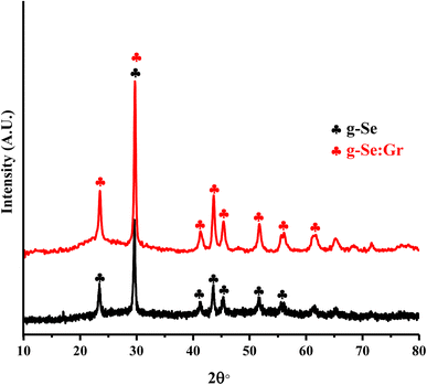 |
| | Fig. 1 XRD spectra of g-Se and g-Se:Gr nanocomposite samples. | |
Table 1 Average crystallite size, strain, and dislocation density for g-Se:Gr nanocomposite
| Sample |
Crystallite Size (nm) |
Strain (ε) [×10−3] |
Dislocation density (δ) [×10−3 nm−2] |
| g-Se:Gr |
18 |
5.5 |
3.3 |
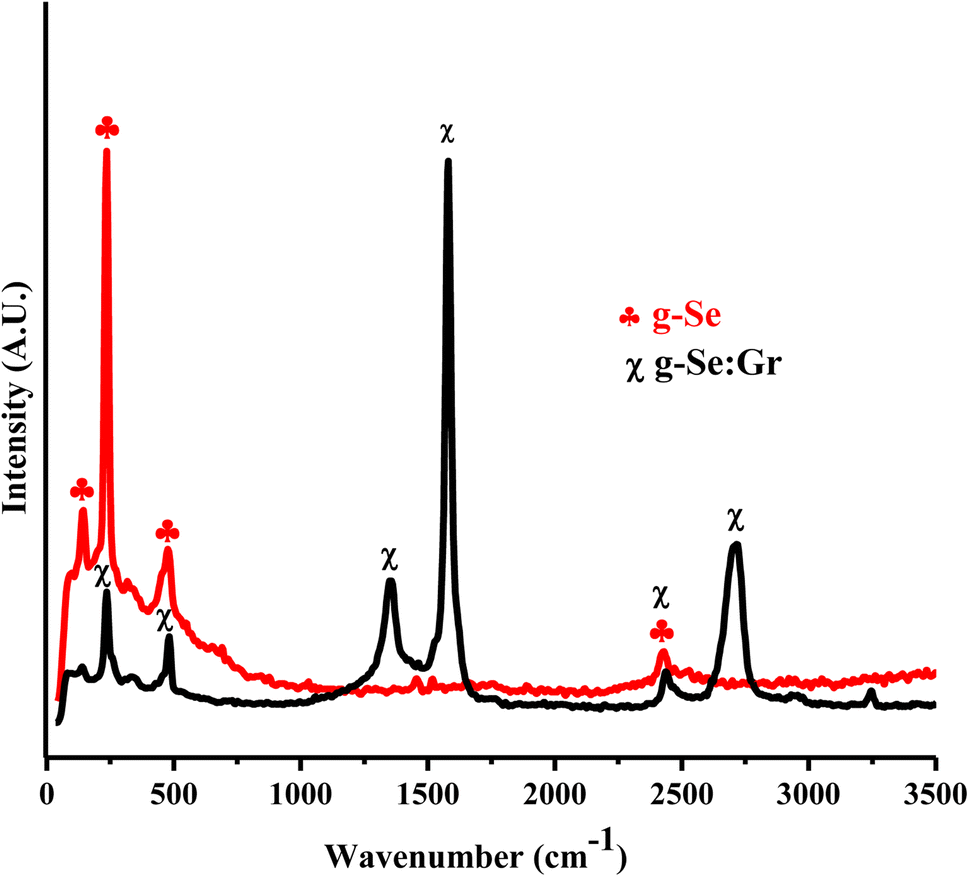
Fig. 2 displays the well-resolved Raman spectra of the as-prepared g-Se and g-Se:Gr nanocomposite. The Raman band at 236.0 cm−1 is associated with the Sen vibration frequency of t-Se51 caused by the vibration of the A1 and E modes which results in the crystalline state of Sen chains. The band peak position at 144.84 cm−1 is assigned to the E1 peak. Another small peak (i.e., second peak) at ∼482 cm−1 is attributed to the vibration modes of resonant t-Se Raman modes. After doping graphene in the host glass matrix, two new bands appear at 1353.8 cm−1 (corresponding to unresolved D3, D, and D4 bands) and 1581.6 cm−1 (corresponding to unresolved G and D′ bands), which are characteristic bands of graphene.52 The central feature of the graphene-doped g-Se nanocomposite is the appearance of the G band at 1581.6 cm−1 that corresponds to the degenerate in-plane E2g optical mode at the center of the Brillouin zone.52 A less intense peak at 1353.8 cm−1, known as the D band, corresponds to a Raman active mode in defective graphitic substances. Defect-induced double resonance scattering events with a contribution of electronic π–π* transitions are responsible for this band. Such events are associated with anatomical imperfections due to out-of-plane vibrations. A broadened band around 2716.1 cm−1 is the second-order harmonic of the D band, i.e., the 2D band, which is used to determine graphene layer thickness and shows its disperse nature.49
 |
| | Fig. 2 Raman spectra of g-Se and g-Se:Gr nanocomposite samples. | |
The XPS survey analysis illustrates the chemical composition and presence of the functional groups of g-Se:Gr nanocomposite. The deconvoluted C 1s spectrum in Fig. 3a depicts the presence of the different carbon chemical forms and the characteristic binding energies of hybridization.53 The deconvoluted C 1s spectrum shows two peak binding energies of 284.6 eV, assigned to a predominant C–C sp2 graphitic structure,54 and 296.85 eV, assigned to σ* C–C sp3 hybridization.55 Fig. 3b shows the high-resolution core level fitted spectrum for Se 3d with a single peak at a binding energy of 55.35 eV, which suggests the presence of an C–Se–C polymeric chain.56 The C 1s and Se 3d core level spectra confirm the presence of carbon in the synthesized glassy nanocomposite in good agreement with the XRD and Raman structural analysis.
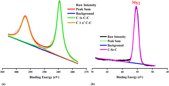 |
| | Fig. 3 High-resolution XPS spectra of (a) C 1s and (b) Se 3d for the g-Se:Gr nanocomposite. | |
Researchers pay a lot of attention to carbon-containing fillers, in which carbon black, nanotubes (CNTs) and graphene are generally used, because they have outstanding electrical characteristics and a moderately low amount can raise the dielectric constant of the host substance.57 It is important to keep in mind, nevertheless, that these composites' dielectric loss will rise concurrently. This is mostly related to leakage current that results from the creation of an electrically conductive route in composites.58 Dielectric measurements provide information about the structural/transport properties of different kinds of dielectric substances (e.g., alloys, composites, and compounds). The dependence of the A/C conductivity on frequency and temperature was investigated for the present novel sample obtained by doping graphene in the host glassy selenium. Alteration in the electric/dielectric parameters of non-crystalline chalcogen-rich glassy materials can be achieved by admixing or doping a conducting dopant. The dispersion of a conductive filler in a polymer matrix at which a conducting framework will develop at a definite concentration is recognized as the percolation threshold.59 The degree of dispersion of the filler inside the polymer matrix determines the exceptional properties of percolative polymeric nanocomposites. We studied the frequency (1 kHz–1 MHz) and temperature (303–333 K) dependence of the dielectric constant and loss (Fig. 4 and 5). The results show that orientational polarization has the dominant contribution while dielectric loss is related to the conduction losses.60 Fig. 4 shows that the dielectric constant (ε′) decreases for both samples with the rising frequency as a result of the drop in the space charge polarization effects.61 The dielectric constant of a dielectric sample is influenced by polarisation, which results from the dipoles' directional alignment. Due to the altered frequency of the applied electric field, the orientation of the dipoles is reversed. Due to the material's resistance and the rate of increasing frequency, the dipoles are unable to align themselves with changes in the electric field, leading to the relaxation phenomenon. The alignment of the dipoles ceases at the maximum applied frequency, resulting in no contribution to the permittivity.62,63 At room temperature (303 K), the value of the dielectric constant of g-Se:Gr nanocomposite rises drastically compared to that of g-Se and is shown at three different audio frequencies in Fig. 4b. This figure shows that the dielectric constant rises almost ten to twelve-fold after the incorporation of graphene into the host material (i.e., g-Se). The formation of large electric dipoles per unit volume occurs in g-Se:Gr as the graphene sheets play the role of fillers.64 Consequently, the dielectric constant of g-Se:Gr becomes larger than that of g-Se.64 Charge carriers are transferred through the bulk glassy network by the mobility of the polymeric chain and the mobility of charge carriers is also influenced by the interfacial interaction between the polymer matrix and graphene, which raises the dielectric constant of the present nanocomposite.65,66 The energy attenuation corresponding to dielectric loss (ε′′) is related to lagging with respect to the applied electric field that is triggered by the grain boundaries during the dielectric relaxation process.61 Fig. 5 depicts the plots of the dielectric loss as a function of the rising frequency at room temperature for the present samples. The experimental curves demonstrate the fall in dielectric loss with the rise in applied angular frequency. The high value of ε′′ at a lower frequency is a consequence of the high resistivity of grain boundaries, which are more efficient than the grains. Due to the lack of direct connection between the graphene sheets in the glass matrix, there is an exfoliated dispersion of graphene in the glassy network, which can also be inferred from the SEM micrograph and is probably responsible for the observed increases in both dielectric parameters.66,67 The simultaneous achievement of a high dielectric constant and low dielectric loss is challenging. Therefore, it is important to control the interaction between the graphene layers and the glassy environment corresponding to long polymeric selenium chain matrices to optimize the dielectric constant and loss in the derived sample for energy storage applications68 in the near future.
 |
| | Fig. 4 (a) Frequency dependence of dielectric constant (ε′) for g-Se:Gr and (b) frequency-dependent comparative study of dielectric constant at 303 K for g-Se and g-Se:Gr samples. | |
 |
| | Fig. 5 Frequency dependence of dielectric loss (ε′′) at 303 K. The left and right hand sides correspond to g-Se and g-Se:Gr samples, respectively. | |
The frequency dependence of AC conductivity (σac) is governed by the following relation.
Here,
ε0 is the permittivity of free space,
ε′′ is the dielectric loss, and
ω is the angular frequency. The comparison of
σac for the present samples at three different frequencies is shown in
Fig. 6. The increase in conductivity with increasing frequency is attributed to the hopping mechanism that appears when applying the electric field.
69 Hopping conduction is the dominant mechanism of charge carriers in a disordered graphene-doped composite when they percolate between the free delocalized states. Their hopping between the offered states is responsible for the corresponding transport properties.
70 The simulations and experimental findings by various research groups demonstrate that conductive fillers with a larger aspect ratio lead to a reduced percolation threshold and higher conductivity. When the filler content reaches the percolation threshold, a connected conductive network creates a route for electronic transport and an insulator is turned into a semiconductor.
59,71
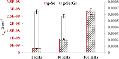 |
| | Fig. 6 Plot showing the comparative frequency dependence and AC conductivity (σac) at 303 K for g-Se and g-Se:Gr samples. | |
We performed calorimetric experiments using the DSC technique to measure the characteristic temperatures of interest (e.g., glass transition temperature Tg and crystallization temperature Tc) for g-Se and g-Se:Gr; the results are listed in Table 2. From the single glass transition peaks that appeared in the DSC scans (Fig. 7), we observe that no phase separation occurs after the doping of graphene in the host material. This confirms the good miscibility of graphene in the glass matrix of host g-Se after melt quenching. Further, we observe the shifting of the glass transition and crystallization peaks to lower temperature values. Since g-Se consists of polymeric chains of Se with dangling bonds, the dispersion of graphene in the g-Se network interferes with the radius of gyration of these polymeric chains. Consequently, the free volume increases and the glass network of g-Se:Gr acts like a plasticizer. Due to this, the glass transition temperature (Tg) decreases after the addition of graphene in the host g-Se.72 The higher specific heat of graphene compared to that of g-Se facilitates the g-Se:Gr to crystallize more rapidly than g-Se. Thus, the To and Tc values of g-Se:Gr nanocomposite are shifted lower, which reduces the crosslinking density in the polymeric network, resulting in increased mobility of the structural units in the glassy nanocomposite.73
Table 2 Transition temperatures of g-Se and g-Se:Gr samples at a heating rate of 10 K min−1
| Sample |
Tg (K) |
Tc (K) |
To (K) |
Tm (K) |
TS |
Hr |
| g-Se |
324.7 |
386.7 |
376.4 |
495.2 |
1.9 |
0.4 |
| g-Se:Gr |
320.6 |
373 |
346.3 |
495 |
4.3 |
0.5 |
 |
| | Fig. 7 (a) DSC scans of as-prepared g-Se and g-Se:Gr samples at a heating rate of 10 K min−1 and (b) comparative analysis of crystallization activation energies for g-Se and g-Se:Gr samples. | |
The two significant parameters that are directly linked to optical memory applications74,75 of such phase transition materials are thermal stability and glass-forming ability. The thermal stability (S) is a parameter that reflects the resistance to devitrification after formation of the glass; it can be calculated using the following expression.76
| |
 | (2) |
Hruby proposed an empirical relation known as the Hruby number which is a strong indicator of the glass-forming tendency and is calculated from the following expression.76
| |
 | (3) |
Here,
To and
Tm are the onset crystallization and melting temperatures, respectively (
Table 2). The values of the
S and
HR parameters were deduced and are included in
Table 2. The activation energies
Ec and
Eg corresponding to the phase transitions at
Tc and
Tg were determined using non-isothermal DSC data by a non-isothermal procedure and are listed in
Table 3. The presence of graphene in the polymer matrix caused the uniform distribution of applied thermal energy which could be attributed to the 2D structure and enhanced the effective surface area of the nanocomposite.
77 The observed increase of
Ec due to the graphene doping (
Fig. 7b) in the parent sample increased the thermal stability of the glassy nanocomposite because
Ec denotes the energy required by the atoms in the glassy region to go into the crystalline region.
78
Table 3 Glass transition activation energy (Eg) and crystallization activation energy (Ec) of g-Se and g-Se:Gr samples
| Sample |
Eg (kJ mol−1) |
Ec (kJ mol−1) |
| Kissinger method |
Moynihan method |
Kissinger method |
Augis–Bennett method |
Matusita–Sakka method |
| g-Se |
218.6 |
224 |
92.9 |
96.1 |
99.4 |
| g-Se:Gr |
352.9 |
358.2 |
120.5 |
123.6 |
126.7 |
The SEM micrographs provide surface morphological and structural information on the graphene-doped g-Se. SEM images of g-Se and g-Se:Gr are shown in Fig. 8a and b, indicating the non-crystalline nature of g-Se and the formation of crystallites in significant amounts in the glass network of g-Se after the doping of graphene. From the SEM micrographs, it can be concluded that the distorted edge configuration of graphene nanosheets embedded in the glassy host matrix of Se, and it is responsible for the higher charge carrier mobility.79 The cross-linked structural arrangement of nanosheets within the matrix can provide a path for electronic conduction and tailor the physical properties of g-Se due to nanoscale structural entities that can be inferred from the SEM micrograph. In this way, the structural characterizations reveal the same observation: that graphene sheets are successfully rooted in the parent sample (Fig. 9). While the origin of the precise mechanism responsible for the observed structural miscibility of graphene into g-Se is not recognized at this point, we hope that it will be revealed in the near future.
 |
| | Fig. 8 SEM micro-images of as-prepared g-Se and g-Se:Gr samples. | |
 |
| | Fig. 9 Schematic illustration of plausible structural rearrangement after the doping of graphene in glassy selenium. | |
The current–voltage (I–V) characteristics of the g-Se:Gr sample were studied in different electric fields (∼104 V cm−1). Fig. 10 shows the I–V characteristics for the as-prepared samples of elemental selenium glass and g-Se:Gr which reveal an abrupt change (i.e., 3.93 × 10⁻⁶ ampere to 2.1 × 10⁻² ampere) in the electric current near the threshold switching voltage of 42.5 volts for the g-Se:Gr nanocomposite. The drop in threshold voltage Vth after the doping of graphene in g-Se is probably related to the connection between Vth and crystal growth velocity vcg.80 The shifting of the crystallization peak towards a lower Tc value in g-Se:Gr compared to g-Se indicates that vcg is increased after the incorporation of graphene in the amorphous matrix of g-Se. This causes a rapid reduction in the amorphous regions of g-Se:Gr and so the current enters the non-ohmic region at a lower threshold voltage Vth. This indicates that the material has switched from a high resistance state (HRS) to a low resistance state (LRS) after the doping of graphene in the polymeric glass network under the influence of an appropriate external electric field.81 The DC conductivity of the g-Se:Gr nanocomposite was investigated as a function of reciprocal temperature. The variation of ln![[thin space (1/6-em)]](https://www.rsc.org/images/entities/char_2009.gif) σdc vs. 1000/T follows a straight line, indicating a thermally activated mechanism. From Fig. 11, it is clear that the σdc increases linearly with the decreasing reciprocal of absolute temperature. The thermal activation energy and DC conductivity were calculated using the Arrhenius relation.
σdc vs. 1000/T follows a straight line, indicating a thermally activated mechanism. From Fig. 11, it is clear that the σdc increases linearly with the decreasing reciprocal of absolute temperature. The thermal activation energy and DC conductivity were calculated using the Arrhenius relation.
| |
 | (4) |
Here,
σ0 and Δ
E indicate the pre-exponential factor and activation energy, respectively. It was found that the conductivity increases with the admixing of graphene. The electrical parameters for the present samples are tabulated in
Table 4. The incorporation of graphene in g-Se causes a rise in the hopping of the charge carriers between the neighbouring sites. The magnitude of Δ
E also depends on the number of π-electrons existing in the semiconducting material and possesses a temperature dependence on DC conductivity according to the Arrhenius relation. The value of Δ
E decreases with a rise in the number of π-bonds. The further reduction in the value of Δ
E after the doping of graphene suggests that there are some partial double bonds between carbon and selenium (possibly due to π-back donations). The augmentation in electrical conductivity compared to g-Se could be attributed to the extended π-electron system in the hexagonal structural units contributing to high conductivity and increased mobility, which creates a percolation path in g-Se:Gr where the electrons in the graphene surface have long mean free paths without disrupting electron–electron interactions and surface disorder.
82 The incorporated a-Se in the form of cyclic Se
8 molecules in the pores of carbon was converted into chain-like Se
n molecules when selenium was mixed with graphene, ensuring improved electronic transport.
83,84 Using first principles calculations, the bonding of a selenium atom to the surface edge defect sites of the graphene nanosheets leads to the enhancement of electrical conductivity due to p-type doping.
85 Sharma
et al. suggested that, since selenium has more valence electrons than do carbon atoms and these interfacial Se electrons adsorb on the graphene surface, occupying high-energy states of hybridization with the graphene sheet and leading to a positive shift of the Dirac point (where the valence band (VB) and conduction band (CB) intersect with minimum conductivity), this is an indication of an n-type conducting material and hence shows improved electrical conductivity due to surface charge doping.
86 The incorporation of graphene in g-Se causes a rise in the density of defect states in the valence band which is responsible for the shifting of the band edge towards lower energy. Consequently, the localization of additional density of states in g-Se:Gr near the bandgap reduces the mobility gap. This improves the thermally activated hopping and leads to enhanced conductivity.
 |
| | Fig. 10 Switching characteristics of (a) g-Se sample and (b) g-Se:Gr sample under high field (∼104 V cm−1). | |
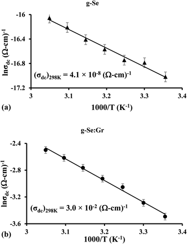 |
| | Fig. 11 Arrhenius plots of electrical conductivity σdc showing the temperature dependence for (a) g-Se and (b) g-Se:Gr samples. The room temperature values of σdc are shown below the linear curves. | |
Table 4 Electrical parameters for g-Se and g-Se:Gr samples (303 K, 100 kHz)
| Sample |
σac (Ω cm)−1 (303 K, 100 kHz) |
σdc (Ω cm)−1 (303 K) |
ΔEdc (eV) |
| g-Se |
2.9 × 10⁻⁸ |
4.1 × 10⁻⁸ |
0.26 |
| g-Se:Gr |
5.7 × 10⁻⁴ |
3.0 × 10⁻² |
0.04 |
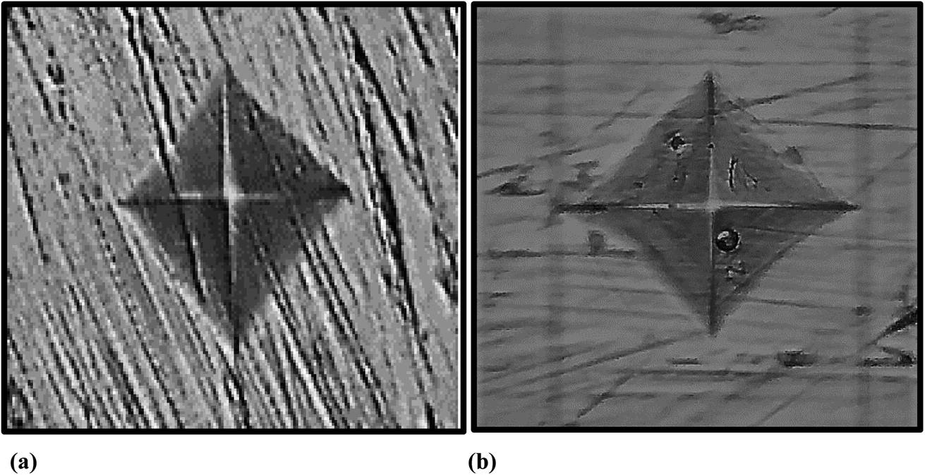
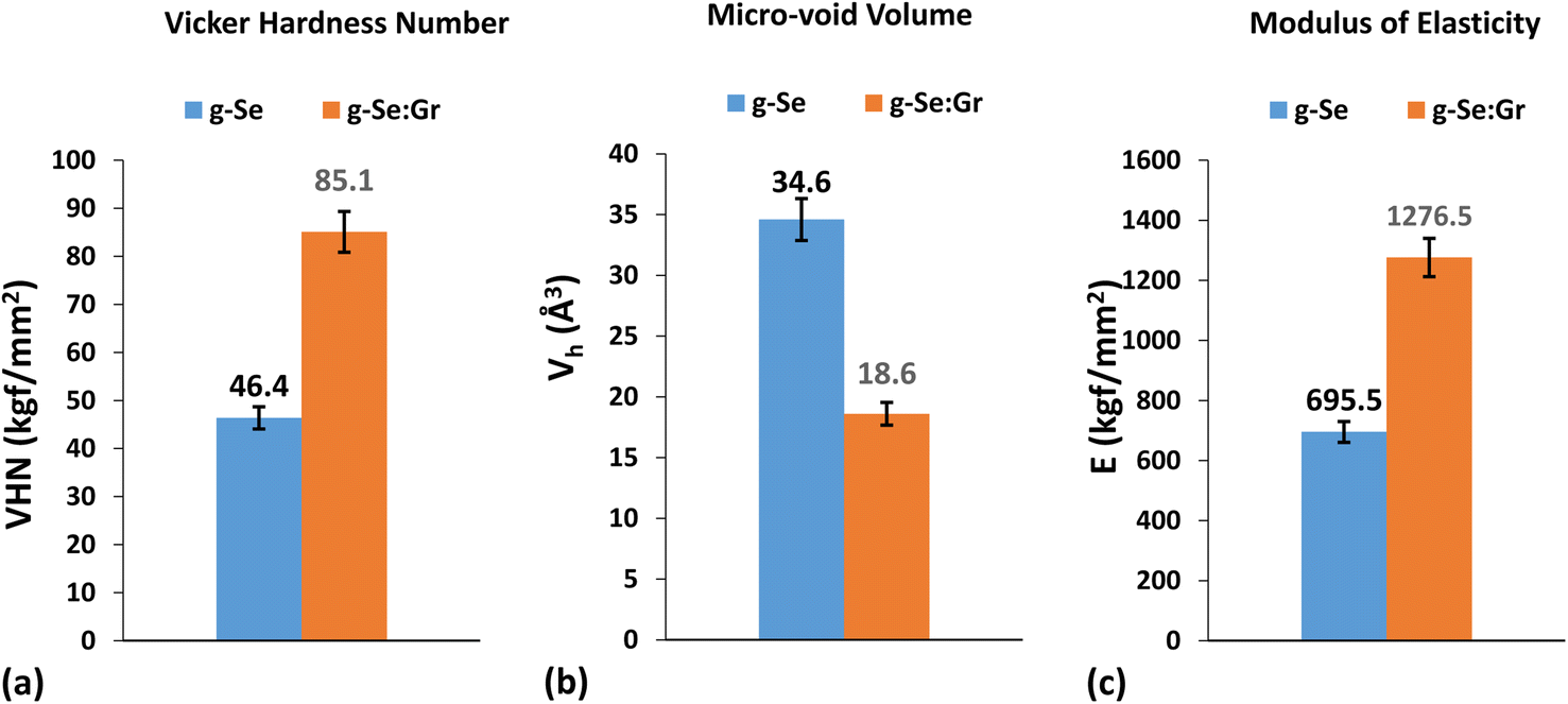
The most striking features of graphene are its enormously high hardness and pliability. Therefore, we measured the micro-hardness of g-Se and g-Se:Gr to understand the effect of graphene doping on the mechanical strength of g-Se. Hardness is a physical attribute of a material defined as the resistance to indentation and is determined by measuring the permanent depth of an indentation. The values of Vickers hardness number (VHN), modulus of elasticity, and micro-voids volume were determined through a micro-indentation experiment.87 Fig. 12 presents a photograph of the micro-indentation impressions on the surfaces of the samples. A close inspection of both impressions reveals that the indentation size is more symmetric for g-Se:Gr. The structural rigidity of the glass matrix of g-Se is increased after the incorporation of graphene.88,89 This results in exactly equal diagonals of the indent marks for g-Se:Gr compared to the almost equal diagonals of the indent marks for g-Se. The values of microhardness, modulus of elasticity, and micro-void volume are shown in Fig. 13 for both samples. In this figure, we observe the rise in the modulus of elasticity and VHN of g-Se after the graphene doping. The increased values of both parameters are probably related to the immense strength of the carbon–carbon bonds, with a fundamental rupture strength of 130 GPa and a Young modulus of 1 TPa.90 During the melt quenching after heat treatment, the doping of graphene facilitates grain refining and activates dislocation between the graphene nanoplatelets within the glass matrix of g-Se.89 Consequently, the direct strengthening occurs due to load transfer from the softer and weaker polymeric selenium chains to the stiff and strong graphene nanoplatelets. This is probably the reason behind the higher values of the Vickers hardness and modulus of elasticity and the lower value of micro-void volume in the case of g-Se:Gr.
 |
| | Fig. 12 Photographs of micro-indentation impressions on the surfaces of (a) g-Se sample and (b) g-Se:Gr nanocomposite sample. | |
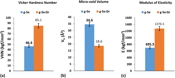 |
| | Fig. 13 Bar graphs showing the comparative values of (a) Vickers hardness number (VHN), (b) volume of micro-voids Vh, and (c) modulus of elasticity E for g-Se and g-Se:Gr samples. | |
4. Conclusions
In this work, we successfully achieved the nano-structuring of g-Se by doping one weight percent graphene. Due to the inherent high electrical conductivity and mechanical strength of the graphene layers, the physical properties of the host glass of selenium are improved drastically. The lack of phase separation is confirmed by calorimetric results that signify the homogeneity of the g-Se:Gr sample. There is a significant rise in glass transition and crystallization activation energies after the inclusion of graphene in elemental selenium glass. Similarly, there is a noticeable rise in the dielectric parameters and DC/AC conductivities. The I–V characteristic plots show a rapid growth in the current with a slight increase in the voltage after the doping of graphene in host g-Se. Resistive-switching is observed after a certain voltage (i.e., threshold voltage Vth) in both samples. A remarkable drop in the Vth value is noticed after the graphene doping in g-Se. The structural analyses of SEM and Raman experiments confirm the nano-structuring of g-Se with the help of graphene as a dopant and the noticeable change in various physical properties of the derived material g-Se:Gr. The current findings can serve as a foundation for more in-depth research to develop this new material for application in optical memory and energy storage technologies.
Conflicts of interest
There are no conflicts to declare.
Acknowledgements
Neeraj Mehta is grateful to Banaras Hindu university to provide an incentive grant (Dev. Scheme No. 6031) to buy consumables under the Institutes of Eminence scheme of UGC, New Delhi, India.
References
- H. Yuan, L. Kong, T. Li and Q. Zhang, Chin. Chem. Lett., 2017, 28, 2180–2194, DOI:10.1016/j.cclet.2017.11.038.
- F. Bonaccorso, L. Colombo, G. Yu, M. Stoller, V. Tozzini, A. C. Ferrari, R. S. Ruoff and V. Pellegrini, Science, 2015, 347, 1246501, DOI:10.1126/science.1246501.
- N. S. Shaikh, S. Ubale, V. Mane, J. S. Shaikh, V. Lokhande, S. Praserthdam, C. Lokhande and P. Kanjanaboos, J. Alloys Compd., 2022, 893, 161998, DOI:10.1016/j.jallcom.2021.161998.
- Q. Zhou, X. Qi, Yi. Zhou, J. Li, J. Jiang, H. Li, X. Niu, R.-Z. Wu and J. Chen, J. Alloys Compd., 2023, 942, 168944, DOI:10.1016/j.jallcom.2023.168944.
- J. F. R. V. Silveira, R. Besse and J. L. F. Da Silva, ACS Appl. Electron. Mater., 2021, 4, 1671–1680, DOI:10.1021/acsaelm.1c00009.
- R. N. A. R. Seman, M. A. Azam and M. H. Ani, Nanotechnology, 2018, 29, 502001, DOI:10.1088/1361-6528/aae3da.
- C. Luo, Y. Xu, Y. Zhu, Y. Liu, S. Zheng, Y. Liu, A. Langrock and C. Wang, ACS Nano, 2013, 7, 8003–8010, DOI:10.1021/nn403108w.
- L. Zeng, W. Zeng, Y. Jiang, X. Wei, W. Li, C. Yang, Y. Zhu and Y. Yu, Adv. Energy Mater., 2015, 4, 1401377, DOI:10.1002/aenm.201401377.
- A. Abouimrane, D. Dambournet, K. W. Chapman, P. J. Chupas, W. Weng and K. Amine, J. Am. Chem. Soc., 2012, 134, 4505–4508, DOI:10.1021/ja211766q.
- M. Khan, X. Ding, H. Zhao, Y. Wang, N. Zhang, X. Chen and J. Xu, Electrochem, 2022, 3, 285–308, DOI:10.3390/electrochem3020020.
- X. Peng, L. Wang, X. Zhang, B. Gao, J. Fu, S. Xiao, K. Huo and P. K. Chu, J. Power Sources, 2015, 288, 214–220, DOI:10.1016/j.jpowsour.2015.04.124.
- H. C. Youn, J. H. Jeong, K. C. Roh and K. B. Kim, Sci. Rep., 2016, 6, 30865, DOI:10.1038/srep30865.
- X. Meng, C. Yu, X. Song, J. Iocozzia, J. Hong, M. Rager, H. Jin, S. Wang, L. Huang, J. Qiu and Z. Lin, Angew. Chem., 2018, 130, 4772–4776, DOI:10.1002/ange.201801337.
- S. Yang, J. Sun, P. He, X. Deng, Z. Wang, C. Hu, G. Ding and X. Xie, Chem. Mater., 2015, 27, 2004–2011, DOI:10.1021/acs.chemmater.5b00112.
- K. Han, Z. Liu, J. Shen, Y. Lin, F. Dai and H. Ye, Adv. Funct. Mater., 2015, 25, 455–463, DOI:10.1002/adfm.201402815.
- J. He, Y. Chen, W. Lv, K. Wen, P. Li, Z. Wang, W. Zhang, W. Qin and W. He, ACS Energy Lett., 2016, 1, 16–20, DOI:10.1021/acsenergylett.6b00015.
- D. Huang, S. Li, Y. Luo, X. Xiao, L. Gao, M. Wang and Y. Shen, Electrochim. Acta, 2016, 190, 258–263, DOI:10.1016/j.electacta.2015.12.187.
- K. Han, Z. Liu, H. Ye and F. Dai, J. Power Sources, 2014, 263, 85–89, DOI:10.1016/j.jpowsour.2014.04.027.
- C. P. Yang, S. Xin, Y. X. Yin, H. Ye, J. Zhang and Y. G. Guo, Angew. Chem., Int. Ed., 2013, 52, 8363–8367, DOI:10.1002/anie.201303147.
- J. Zhang, L. Fan, Y. Zhu, Y. Xu, J. Liang, D. Wei and Y. Qian, Nanoscale, 2014, 6, 12952–12957, 10.1039/C4NR03705G.
- Z. Li, L. Yuan, Z. Yi, Y. Liu and Y. Huang, Nano Energy, 2014, 9, 229–236, DOI:10.1016/j.nanoen.2014.07.012.
- S. Jiang, Z. Zhang, Y. Lai, Y. Qu, X. Wang and J. Li, J. Power Sources, 2014, 267, 394–404, DOI:10.1016/j.jpowsour.2014.05.116.
- Y. Qu, Z. Zhang, S. Jiang, X. Wang, Y. Lai, Y. Liu and J. Li, J. Mater. Chem. A, 2014, 2, 12255–12261, 10.1039/C4TA02563F.
- Y. Liu, L. Si, X. Zhou, X. Liu, Y. Xu, J. Bao and Z. Dai, J. Mater. Chem. A, 2014, 2, 17735–17739, 10.1039/C4TA03141E.
- Y. Lai, Y. Gan, Z. Zhang, W. Chen and J. Li, Electrochim. Acta, 2014, 146, 134–141, DOI:10.1016/j.electacta.2014.09.045.
- J. Zhang, Z. Zhang, Q. Li, Y. Qu and S. Jiang, J. Electrochem. Soc., 2014, 161, A2093, DOI:10.1149/2.0451414jes.
- H. Zhang, F. Yu, W. Kang and Q. Shen, Carbon, 2015, 95, 354–363, DOI:10.1016/j.carbon.2015.08.050.
- X. Wang, Z. Zhang, Y. Qu, G. Wang, Y. Lai and J. Li, J. Power Sources, 2015, 287, 247–252, DOI:10.1016/j.jpowsour.2015.04.052.
- Z. Yi, L. Yuan, D. Sun, Z. Li, C. Wu, W. Yang, Y. Wen, B. Shan and Y. Huang, J. Mater. Chem. A, 2015, 3, 3059–3065, 10.1039/C4TA06141A.
- J. T. Lee, H. Kim, M. Oschatz, D. C. Lee, F. Wu, H. T. Lin, B. Zdyrko, W. Cho, S. Kaskel and G. Yushin, Adv. Energy Mater., 2015, 5, 1400981, DOI:10.1002/aenm.201400981.
- J. Zhang, Y. Xu, L. Fan, Y. Zhu, J. Liang and Y. Qian, Nano Energy, 2015, 13, 592–600, DOI:10.1016/j.nanoen.2015.03.028.
- Y. Liu, L. Si, Y. Du, X. Zhou, Z. Dai and J. Bao, J. Phys. Chem. C, 2015, 119, 27316–27321, DOI:10.1021/acs.jpcc.5b09553.
- Z. Zhang, X. Yang, Z. Guo, Y. Qu, J. Li and Y. Lai, J. Power Sources, 2015, 279, 88–93, DOI:10.1016/j.jpowsour.2015.01.001.
- J. Guo, Q. Wang, C. Qi, J. Jin, Y. Zhu and Z. Wen, Chem. Commun., 2016, 52, 5613–5616, 10.1039/C6CC00638H.
- T. Liu, C. Dai, M. Jia, D. Liu, S. Bao, J. Jiang, M. Xu and C. M. Li, ACS Appl. Mater. Interfaces, 2016, 8, 16063–16070, DOI:10.1021/acsami.6b04060.
- K. Balakumar and N. Kalaiselvi, Carbon, 2017, 112, 79–90, DOI:10.1016/j.carbon.2016.10.097.
- T. Liu, M. Jia, Y. Zhang, J. Han, Y. Li, S. J. Bao, D. Liu, J. Jiang and M. Xu, J. Power Sources, 2017, 341, 53–59, DOI:10.1016/j.jpowsour.2016.11.099.
- J. Zhou, J. Yang, Z. Xu, T. Zhang, Z. Chen and J. Wang, J. Mater. Chem. A, 2017, 5, 9350–9357, 10.1039/C7TA01564J.
- J. Ding, H. Zhou, H. Zhang, L. Tong and D. Mitlin, Adv. Energy Mater., 2018, 8, 1701918, DOI:10.1002/aenm.201701918.
- W. Jin, H. Li, J. Zou, S. Inguva, Q. Zhang, S. Zeng, G. Xu and X. Zeng, J. Alloys Compd., 2020, 820, 153084, DOI:10.1016/j.jallcom.2019.153084.
- M. H. A. Shiraz, Y. Hu and J. Liu, ECS Trans., 2020, 97, 279, DOI:10.1149/09707.0279ecst.
- Z. Lei, Y. Lei, X. Liang, L. Yang and J. Feng, J. Power Sources, 2020, 473, 228611, DOI:10.1016/j.jpowsour.2020.228611.
- Q. Zhang, L. Cai, G. Liu, Q. Li, M. Jiang and X. Yao, ACS Appl. Mater. Interfaces, 2020, 12, 16541–16547, DOI:10.1021/acsami.0c01996.
- P. Xue, Y. Zhai, N. Wang, Y. Zhang, Z. Lu, Y. Liu, Z. Bai, B. Han, G. Zou and S. Dou, Chem. Eng. J., 2020, 392, 123676, DOI:10.1016/j.cej.2019.123676.
- Y. Lei, X. Liang, L. Yang, J. Chen, L. Qu, K. Xu and J. Feng, Carbon, 2022, 191, 122–131, DOI:10.1016/j.carbon.2022.01.053.
- M. A. R. Fresneda, J. D. Martín, J. G. Bolivar, M. V. F. Cantos, G. B. Estevez, M. F. M. Moreno and M. L. Merroun, Environ. Sci.: Nano, 2018, 5, 2103–2116, 10.1039/C8EN00221E.
- A. Kumar and K. S. Prasad, J. Biotechnol., 2021, 325, 152–163, DOI:10.1016/j.jbiotec.2020.11.004.
- A. Chamuah, S. Ojha, K. Bhattacharya, C. K. Ghosh and S. Bhattacharya, J. Phys. Chem. Solids, 2022, 166, 110695, DOI:10.1016/j.jpcs.2022.110695.
- S. K. Yadav, D. Roy, A. K. Yadav, P. Sagar and S. K. Avinashi, J. Therm. Anal. Calorim., 2022, 147, 11661–11670, DOI:10.1007/s10973-022-11388-3.
- C. S. Bagade, S. S. Mali, V. B. Ghanwat, K. V. Khot, P. B. Patil, S. D. Kharade, R. M. Mane, N. D. Desai, C. K. Hong, P. S. Patil and P. N. Bhosale, RSC Adv., 2015, 5, 55658–55668, 10.1039/C5RA08791K.
- M. Marple, J. Badger, I. Hung, Z. Gan, K. Kovnir and S. Sen, Angew. Chem., Int. Ed., 2017, 56, 9777–9781, DOI:10.1002/anie.201704323.
- L. Bokobza, J. L. Bruneel and M. Couzi, C, 2015, 1, 77–94, DOI:10.3390/c1010077.
- B. Lesiak, L. Kover, J. Tóth, J. Zemek, P. Jiricek, A. Kromka and N. Rangam, Appl. Surf. Sci., 2018, 452, 223–231, DOI:10.1016/j.apsusc.2018.04.269.
- W. Wang, S. Wang, S. Zhang, W. Wang, X. Ji and C. Li, RSC Adv., 2020, 10, 12060–12067, 10.1039/C9RA08905E.
- J. Lomon, P. Chaiyabin, T. Saisopa, K. Seawsakul, N. Saowiang, K. Promsakha, P. Poolcharuansin, N. Pasaja, A. Chingsungnoen and R. Supruangnet, J. Phys.: Conf. Ser., 2018, 1144, 012048, DOI:10.1088/1742-6596/1144/1/012048.
- Y. Deng, L. Gong, Y. Pan, X. Cheng and H. Zhang, Nanoscale, 2019, 11, 11671–11678, 10.1039/C9NR00701F.
- C. Y. Lee and C. W. Chang, J. Compos. Sci., 2021, 5, 52, DOI:10.3390/jcs5020052.
- M. Li, Y. Deng, Y. Wang, Y. Zhang and J. Bai, Mater. Chem. Phys., 2013, 139, 865–870, DOI:10.1016/j.matchemphys.2013.02.045.
- A. J. Marsden, D. G. Papageorgiou, C. Vallés, A. Liscio, V. Palermo, M. A. Bissett, R. J. Young and I. A. Kinloch, 2D Materials, 2018, 5, 032003, DOI:10.1088/2053-1583/aac055.
- A. Sharma and N. Mehta, RSC Adv., 2017, 7, 19085–19097, 10.1039/C7RA00010C.
- C. Rayssi, S. El. Kossia, J. Dhahri and K. Khirouni, RSC Adv., 2018, 8, 17139–17150, 10.1039/C8RA00794B.
- S. S. Fouad and H. E. Atyia, J. Alloys Compd., 2016, 688, 1206–1213, DOI:10.1016/j.jallcom.2016.07.091.
- A. Srivastava and N. Mehta, J. Alloys Compd., 2016, 658, 533–542, DOI:10.1016/j.jallcom.2015.10.163.
- L. J. Romasanta, M. Hernandez, M. Lopez-Manchado and R. Verdejo, Nanoscale Res. Lett., 2011, 6(1–6), 508, DOI:10.1186/1556-276X-6-508.
- A. Yang, S. J. Hao, S. L. Dai and X. Y. Zhang, Carbon, 2017, 117, 301–312, DOI:10.1016/j.carbon.2017.03.004.
- K. Yang, X. Huang, Y. Huang, L. Xie and P. Jiang, Chem. Mater., 2013, 25, 2327–2338, DOI:10.1021/cm4010486.
- U. O. Uyor, A. P. Popoola, O. Popoola and V. S. Aigbodion, Adv. Polym. Technol., 2018, 37, 2838–2858, DOI:10.1002/adv.21956.
- P. Xu, H. Gui, X. Wang, Y. Hu and Y. Ding, Compos. Sci. Technol., 2015, 117, 282–288, DOI:10.1016/j.compscitech.2015.06.023.
- A. Kumar and N. Mehta, J. Mater. Sci.: Mater. Electron., 2017, 28, 5634–5644, DOI:10.1007/s10854-016-6234-2.
- A. Mobius, Crit. Rev. Solid State
Mater. Sci., 2019, 44, 1–55, DOI:10.1080/10408436.2017.1370575.
- J. Zhang, J. Qiu and J. Liu, Rev. Adv. Sci. Eng., 2014, 3, 48–65, DOI:10.1166/rase.2014.1052.
- N. R. Jadhav, V. L. Gaikwad, K. J. Nair and H. M Kadam, Asian J. Pharm., 2009, 3, 82–89, DOI:10.22377/ajp.v3i2.246.
- K. S. Kim, I. Y. Jeon, S. N. Ahn, Y. D. Kwon and J. B. Baek, J. Mater. Chem., 2011, 21, 7337–7342, 10.1039/C0JM03504A.
- N. Mehta, Rev. Adv. Sci. Eng., 2015, 4, 173–182, DOI:10.1166/rase.2015.1087.
- N. Mehta, Advances in Chalcogenide Glasses (ChGs): Past, present and Future Applications, in Advances in Glass Research, ed. S. J. Ikhmayies, Springer, 2022, pp 153–168, DOI:10.1007/978-3-031-20266-7_5.
- N. Mehta, R. S. Tiwari and A. Kumar, Mater. Res. Bull., 2006, 41, 1664–1672, DOI:10.1016/j.materresbull.2006.02.024.
- P. Manafi, I. Ghasemi, M. Karrabi, H. Azizi, M. R. Manafi and P. Ehsaninamin, Polym. Bull., 2015, 72, 1095–1112, DOI:10.1007/s00289-015-1325-4.
- K. S. Deepika and N. S. S. Rathore, New J. Glass Ceram., 2012, 2, 23–33, DOI:10.4236/njgc.2012.21005.
- A. Bellunato, H. A. Tash, Y. Cesa and G. F. Schneider, ChemPhysChem, 2016, 17, 785–801, DOI:10.1002/cphc.201500926.
- A. Sebastian, M. Le Gallo and D. Krebs, Nat. Commun., 2014, 5, 4314, DOI:10.1038/ncomms5314.
- S. K. Pal, A. Srivastava and N. Mehta, J. Alloys Compd., 2019, 806, 660–667, DOI:10.1016/j.jallcom.2019.07.280.
- M. Sang, J. Shin, K. Kim and K. J. Yu, Nanomaterials, 2019, 9, 374, DOI:10.3390/nano9030374.
- C. P. Yang, S. Xin, Y. Yin, H. Ye, J. Zhang and Y. Guo, Angew. Chem., 2013, 52, 8363–8367, DOI:10.1002/anie.201303147.
- K. Balakumar and N. Kalaiselvi, Carbon, 2017, 112, 79–90, DOI:10.1016/j.carbon.2016.10.097.
- K. Nakada and A. Ishii, Solid State Commun., 2011, 151, 13–16, DOI:10.1016/j.ssc.2010.10.036.
- V. Sharma, D. Mitlin and D. Datta, Langmuir, 2021, 37, 2029–2039, DOI:10.1021/acs.langmuir.0c02893.
- A. Kumar, N. Mehta and A. Dahshan, Mater. Today Commun., 2021, 26, 101719, DOI:10.1016/j.mtcomm.2020.101719.
- D. G. Papageorgiou, I. A. Kinloch and R. J. Young, Prog. Mater. Sci., 2017, 90, 75–127, DOI:10.1016/j.pmatsci.2017.07.004.
- O. Guler and N. Bagci, J. Mater. Res. Technol., 2020, 9, 6808–6833, DOI:10.1016/j.jmrt.2020.01.077.
- C. Lee, X. Wei, J. W. Kysar and J. Hone, Science, 2008, 321, 385–388, DOI:10.1126/science.1157996.
|
| This journal is © The Royal Society of Chemistry 2023 |
Click here to see how this site uses Cookies. View our privacy policy here. 
 Open Access Article
 This Open Access Article is licensed under a Creative Commons Attribution-Non Commercial 3.0 Unported Licence
 ab and
N. Mehta
ab and
N. Mehta