
 Open Access Article
 This Open Access Article is licensed under a Creative Commons Attribution-Non Commercial 3.0 Unported Licence
Microstructure-driven electrical conductivity optimization in additively manufactured microscale copper interconnects†
Maxence Menétrey‡
 a,
Cathelijn van Nisselroy‡b,
Mengjia Xub,
Julian Hengstelerb,
Ralph Spolenak*a and
Tomaso Zambelli*b
a,
Cathelijn van Nisselroy‡b,
Mengjia Xub,
Julian Hengstelerb,
Ralph Spolenak*a and
Tomaso Zambelli*b
aLaboratory for Nanometallurgy, Department of Materials, ETH Zürich, Vladimir-Prelog-Weg 1-5/10, 8093 Zürich, Switzerland. E-mail: ralph.spolenak@mat.ethz.ch
bLaboratory of Biosensors and Bioelectronics, Department of Information Technology and Electrical Engineering, ETH Zürich, Gloriastrasse 35, 8092 Zürich, Switzerland. E-mail: ztomaso@ethz.ch
First published on 3rd May 2023
Abstract
As the microelectronics field pushes to increase device density through downscaling component dimensions, various novel micro- and nano-scale additive manufacturing technologies have emerged to expand the small scale design space. These techniques offer unprecedented freedom in designing 3D circuitry but have not yet delivered device-grade materials. To highlight the complex role of processing on the quality and microstructure of AM metals, we report the electrical properties of micrometer-scale copper interconnects fabricated by Fluid Force Microscopy (FluidFM) and Electrohydrodynamic-Redox Printing (EHD-RP). Using a thin film-based 4-terminal testing chip developed for the scope of this study, the electrical resistance of as-printed metals is directly related to print strategies and the specific morphological and microstructural features. Notably, the chip requires direct synthesis of conductive structures on an insulating substrate, which is shown for the first time in the case of FluidFM. Finally, we demonstrate the unique ability of EHD-RP to tune the materials resistivity by one order of magnitude solely through printing voltage. Through its novel electrical characterization approach, this study offers unique insight into the electrical properties of micro- and submicrometer-sized copper interconnects and steps towards a deeper understanding of micro AM metal properties for advanced electronics applications.
1 Introduction
Additive manufacturing (AM) has become a widespread manufacturing strategy by offering unique opportunities in the way materials are designed and manufactured. While AM of macroscopic parts readily entered the stage of industrial fabrication, the path towards AM of micro- and nanoscale objects currently is a flourishing field of research,1,2 opening the door to breakthrough innovations in the design of microelectronics, such as complex conductive circuits,3,4 or 3D micro-sensors.5,6 Nonetheless, for AM to make a significant impact in the fabrication of such components, it has to deliver conductive elements with well-controlled resistivity. In metals, this property is dictated by electron scattering and can be empirically approximated as the sum of the contributions of individual scattering mechanisms. In bulk materials, scattering events occur primarily due to impurities, thermal vibrations, and lattice defects (grain boundaries, dislocations, point defects). In small objects, however, scattering at interfaces (i.e. surfaces) further impacts the electrical performance as soon as one dimension is on the order of the electron mean free path.7 This phenomenon, known as the classical size effect, leads to inferior electrical performance in downsized electronics and microscale devices of particular interest in the semiconductor industry.8 For nanometer-sized conductors, the electron scattering is dominated by interfacial scattering which is generally described by the Fuchs and Sondheimer (FS) model, and grain boundary scattering where Mayadas and Shatzkes (MS) model9 is widely applied to explain resistivity.10To date, microscale AM methods are not ready to deliver materials competing at the same time with the resolution of lithography processes and the purity of thin film deposition technologies. Nonetheless, particle-based transfer techniques generally achieve crystalline microstructure (despite the presence of pores) after annealing, and electrochemistry-based techniques display as-deposited dense and crystalline metal microstructures with mechanical properties reaching that of thin film technologies.11 Moreover, the extensive microstructure tuning reported by micro AM techniques appears to be a unique asset, first by offering potential in terms of materials optimization, and second by allowing spatial modulations in properties though on-the-fly adjustments in processing parameters.12,13 Thus, to take advantage of this opportunity and make the step towards microelectronics application, an advanced understanding of the causal relationship that link printing strategy, processing parameters to the resulting electrical performance is required. Despite this critical need, no study has undertaken such comprehensive approach. Instead, the majority of scientific work touching upon electrical properties of micro AM objects report on a limited amount of data; often only a single line or pillar is characterized (Table 1). What is further missing for such a study is a standardized measurement template allowing fair comparison between printed microscale conductors.
| Method | Metal | Resistivity μΩ cm | Larger than bulk (ca.) | Measurement configuration | Smallest dim. (ca.) μm | Ref. |
|---|---|---|---|---|---|---|
| a The resistivity can be tuned up to three orders of magnitude (with respect to bulk silver) by changing the laser intensity.b The value or information is not reported. | ||||||
| EHD | Au | 5–20 | 2.5–10 | 4-Terminal | 0.2 | 18 |
| Au | 88 | 36 | 2-Terminal | 0.5 | 17 | |
| Ag | 30 | 20 | 2-Terminal | 1.7 | 16 | |
| Cu | 5.98–24.2 | 3–15 | 2-Terminal | 0.1 | 15 | |
| LIFT | Cu | 18.7–35.3 | 11–22 | 2-Terminal | 2.2 | 24 |
| Ag | 1.9 | 1.2 | 4-Terminal | 5.0 | 23 | |
| DIW | Ag | 5.4 | 3.5a | 4-Terminal | 15 | 13 |
| Ag | 5 | 3 | b | 25 | 20 | |
| Ag | 5–9.5 | 3–6 | 2-Terminal | 4 | 21 | |
| Cu | 3.2 | 2 | 2-Terminal | b | 22 | |
| MCED | Cu | 1150 | 680 | 4-Terminal | 0.5 | 25 |
| Cu | 649 | 389 | 2-Terminal | 11 | 26 | |
| Cu | 31.5 | 19 | 4-Terminal | 0.5 | 27 | |
| Cu | 39 | 23 | 2-Terminal | 1 | 30 | |
| Cu | 3.1 | 1.9 | 2-Terminal | 0.74 | 29 | |
| Cu | 63.6 | 38 | 2-Terminal | 0.76 | 28 | |
| EHD-RP | Cu | 14.4 | 8.6 | 2-Terminal | 0.15 | 32 |
| Cu | 70–555 | 41–330 | 4-Terminal | 0.14 | This study | |
| FluidFM | Cu | 30–662 | 18–394 | 4-Terminal | 0.9 | This study |
We here report on the electrical characterization of copper micro- and submicrometer-sized interconnects printed by two different microscale AM techniques—namely FluidFM and EHD-RP. The introduction of a standardized thin film-based electrode testing chip allows reliable comparison of electrical properties, attributed to different printing strategies, and deposited metal microstructures. Notably both techniques, despite relying on an electrochemical reduction and therefore an electrical current, achieve the deposition of conductive structures on and across an insulating substrate. Finally, following the recent report on precise grain-size control by EHD-RP and its influence on mechanical properties,12 we demonstrate, how similar strategies can be employed to extensively tune the as-deposited copper resistivity. In order to introduce the background of the study, we first provide a short review of the electrical properties of metal micro-objects fabricated by various state-of-the-art micro AM techniques.
1.1 Review on electrical conductivity of microscale metal AM
In the scope of comparing electrical performance, microscale metal AM methods can be advantageously categorized into transfer techniques (relying on the local deposition of pre-synthesized materials) and synthesis techniques (where materials are synthesized in situ from metal ions or other precursors) because the microstructure of the deposit strongly depends on the fabrication type.1 The resistivity values reported in the literature for metal synthesized by micro AM techniques are summarized in Table 1.Transfer techniques mostly lead to the deposition of particles aggregates and thus require an annealing step in order to approach bulk properties.11 Electrohydrodynamic (EHD) printing of inks is based on the rapid ejection of nanodroplets containing metal nanoparticles from a pipette nozzle.14 Upon impact on the substrate, the volatile components of the ink evaporate, leaving as-deposited nanoparticles behind. In this manner, copper tracks, silver bridges and gold wires were 3D printed with resistivity values about one order of magnitude higher than bulk.15–17 Recently, fabrication and electrical characterization of high-aspect-ratio gold nanowalls under atmospheric conditions were reported.18 After sintering, the nanowalls exhibited a resistivity approaching bulk gold. Ejection of silver nanoparticles-loaded inks by direct ink writing (DIW) resulted in the 3D printing of various geometries with applications in radio-frequency (RF)- and microelectronics, with resistivity values of 3× to 15× bulk silver.19–21 As a mean to extend materials properties tunability, laser-assisted DIW—combining DIW with local on-the-fly laser sintering—allowed for the fabrication of segmented silver wires with tailored electrical resistivity ranging from three up to three orders of magnitude larger than bulk.13 Additionally, electroless deposition (ELD) assisted DIW of copper 3D micro-circuitries reported a resistivity reaching as low as 2× of bulk value.22 Laser-induced forward transfer (LIFT) of nanopastes could produce dense silver voxels of varying dimensions that were stacked to create wirebonds connecting a LED circuit on a polyimide substrate.23 Curing the as-deposited paste at 250 °C for one hour decreased the resistivity by three orders or magnitude, thereby approaching the bulk value (1.2× higher). Microstructural analysis revealed an increase in average grain size with annealing temperature from 70 nm (150 °C) to 200 nm (250 °C) which, together with the removal of organic components detected by thermogravimetric analysis, explained the decrease in resistivity from 6.7 μΩ cm down to 1.9 μΩ cm. In a similar work on LIFT, stacking of solidified copper droplets enabled the fabrication of high aspect-ratio pillars with resistivity values reaching 10× and 30× bulk copper, for deposition in argon atmosphere and air respectively.24
Synthesis techniques, and in particular localized electrodeposition, have the ability to synthesize dense and crystalline metals and do not necessarily require a post-printing annealing step.11 Yet, electrical performance varies considerably among the different works. Copper micro-objects manufactured by meniscus confined electrodeposition (MCED) reported resistivity values ranging from 2 to 3 orders of magnitude larger25,26 down to ≈20× larger27,28 than bulk copper, to as low as just twice bulk resistivity.29 In the latter study, in addition to copper, platinum wirebonds were printed which revealed a linear ohmic behavior at low currents, transitioning to a non-ohmic regime for higher currents due to Joule heating. Recently, 3D printed nanotwinned copper engineered by localized pulsed electrodeposition (LPED) exhibited a remarkable trade-off in mechanical and electrical properties, reaching only ≈20× bulk resistivity.30 Interestingly, the resistivity was nearly half of its direct current (DC) counterpart, which is a pattern also reported for the PED of 2D copper foils.31 Besides the various types of MCED mentioned above, Electrohydrodynamic-Redox 3D Printing (EHD-RP) produced dense and polycrystalline copper lines with the lowest resistivity values of 14.4 μΩ cm, corresponding to 8.6× bulk copper.32
2 Results & discussion
2.1 Working principles
2.2 Substrate with built-in electrodes
To enable facile and standardized comparison of electrical characterization of conductive AM structures, this study designed an electrode chip with 8 sample testing areas (i.e. sub-chips), each of which comprising 9 sets of 4 elongated thin-film electrodes (Fig. 1(a)). A conductive structure is printed across each set of electrodes, Fig. 1(c), allowing 4-terminal electrical characterization, which obviates any contribution of the contact resistance to the measurement. The electrodes gradually diverge towards larger pads which are easily contacted by micro-probes, thereby facilitating parametric studies (72 measurements per chip). These chips are produced via lithography-patterning (Fig. 1(b)) for superior consistency in probe contact as compared to contact electrodes added post-printing by focus ion beam-induced deposition. The design was patterned on a glass substrate for FluidFM—as it relies on an inverted microscope—and on Si3N4-coated Si wafer for the samples printed by EHD-RP. An example of an AM line printed across one of 9 sets of electrodes—together with a schematic of the 4-terminal sensing configuration—is displayed in Fig. 1(d). | ||
| Fig. 1 Schematic of the electrode chip for electrical measurement and its fabrication process. (a) Mask design showing one electrode chip and a zoom-in of one of the 8 sub-chips. (b) Photolithography process. A spincoated glass or Si3N4 wafer is exposed and developed. A 3 nm titanium adhesion layer and a 25 nm gold layer are evaporated. The final lift-off reveals the 5 μm-spaced gold electrode tracks. (c) Optical microscope image of the patterned Si3N4 wafer in the sample testing areas (i.e. printing area). A printed line symbolically represented and spanning across a set of four electrodes illustrates the approach. (d) SEM micrograph showing a copper line printed across one set of measurement electrodes and schematic of the 4-terminal electrical characterization. | ||
2.3 Printing on an insulating substrate—overcoming a paradox
Electrochemical techniques generally require a conductive path to supply the reduction current. A premature conclusion assumes that the two techniques are unable to print on the insulating areas of the substrate spanning between the contact electrodes. However, the electrons required for ions reduction are indirectly provided by a grounded electrode—where the first voxel is deposited—through the ongoing printed line, circumventing this issue.Thus, conductive structures were successfully fabricated across the Si3N4 dielectric regions—spanning between the gold thin-film electrodes—both by FluidFM (Fig. 3) and EHD-RP (Fig. 4). The strategies employed by FluidFM for the structures visible in Fig. 3(b)–(e) consist in lateral print head movements in order to deposit voxels side by side (Fig. 2(b)). This strategy was employed to print either single or multiple layers, and the resulting structures will be referred to as line and wall, respectively. These results prove the potential of the two techniques to print micro- and submicrometer-sized interconnects across insulator gaps. Nevertheless, some of the results—in particular the line break seen in Fig. 3(d)–(e) and S1,† as well as the line constriction seen in Fig. 3(b) and (c)—illustrate important challenges arising from the topological and electrical inhomogeneity of the substrate. Namely, the presence of the electrode films influences the electric field in a way that the field lines bow towards the small radius of curvature at the film edges. Consequently, this phenomenon affects both the droplet trajectory in EHD-RP and the ion migration in FluidFM, and ultimately leads to the apparent line irregularity in the vicinity of the edges. This challenge is inherent to all microscale AM techniques that involve electric fields as a driving force for mass transport. Thus, we present various print strategies with both FluidFM and EHD-RP printing techniques to establish a baseline and fundamental insights for conductivity in electrically driven microscale AM.
 | ||
| Fig. 2 Setup and working principles of (a) FluidFM and (c) EHD-RP and their respective printing strategies ((b) and (d)). (a) The chip substrate (yellow) is laminated with PDMS (white, transparent) to confine the supportive electrolyte droplet. The Pt and Ag/AgCl electrodes are inserted in the droplet cell and, together with the chip substrate (WE) connected to a potentiostat. The FluidFM probe is fully immersed inside the droplet cell. (b) Copper ions are extracted from the hollow AFM tip, reduced locally and, due to the integrated force-feedback (AFM laser path shown in red), the copper structures are printed in a voxel-by-voxel manner across the gold electrode tracks. During printing across the insulating regions, the previously printed voxel serves as local WE. (c) A metal sacrificial anode is immersed in an acetonitrile-filled capillary. A potential difference applied between the anode and the substrate triggers the anode corrosion and leads to the release of solvated metal ions Mz+. Ion-loaded droplets are ejected from the capillary nozzle. Upon landing on the grounded substrate, ions are reduced while the solvent evaporates, giving rise to the deposition of a metal voxel. (d) Double line printing strategy across the 4-terminal patterned substrate. | ||
 | ||
| Fig. 3 SEM micrographs of 60 μm copper lines printed by FluidFM at −0.67 V (vs. Ag/AgCl). (a) Overview of 9 lines spanning across various sets of 4-terminal measurement electrodes. One of them is represented in (b) and shows a successful connection between the gold electrodes, as later confirmed by electrical characterization. (c) Enlarged view of a 5 μm long gap. The line in (d) and the zoom-in in (e) display a line printed with similar parameters but disconnected. (f) SEM images of a partial overview of 3D printed Λ-bridges spanning over glass tracks (dark grey). (g) Λ-bridge construction spanning over the 4 contact electrodes and (h) enlarged top-view of the central arc. Substrate tilts were respectively 45° for (b–e and g), 70° for (f), and 0° for the rest. | ||
2.4 Printing strategies
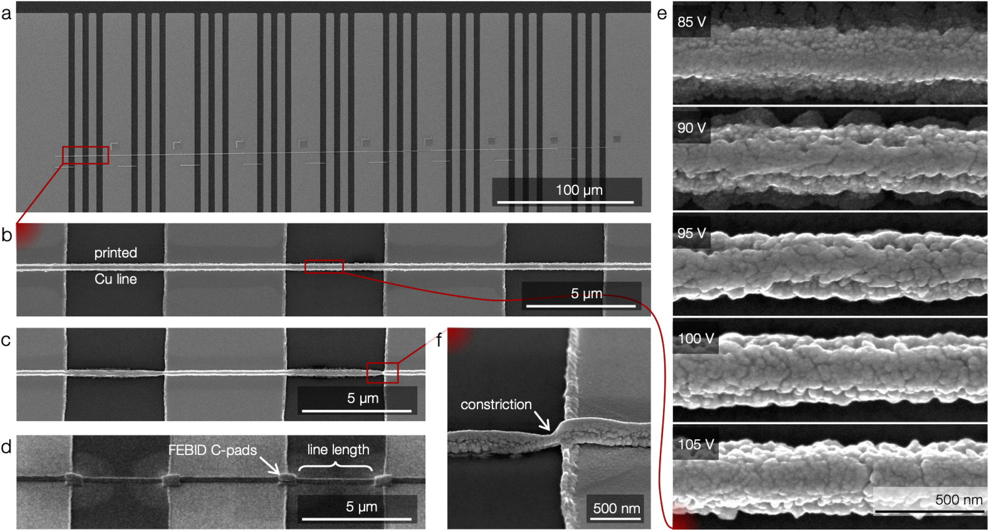 | ||
| Fig. 4 SEM micrographs of sub-micrometer copper lines printed by EHD-RP across the substrate design for 4-terminal-measurement. (a) Overview of the lines across the 9 sets of measurement electrodes using different printing voltages. (b) Enlarged view on a line printed at 105 V and showing a homogeneous section along its length. (c) Line printed at 90 V showing variation in its width and, in particular, (f) a constriction at the transition between the dielectric and conductive substrate. (d) Same line as (c) on which carbon pads were deposited by ion beam-induced deposition to enhance electrical contact reliability. (e) Collection of SEM micrographs showing the direct influence of the printing voltage on the line morphology. Substrate tilts: (a–c and e) 0°, (d) 52°, (f) 55°. | ||
2.5 Morphology, microstructure and resistivity
 | ||
| Fig. 5 Microstructure and electrical resistivity. (d) Measured electrical resistivity resulting from the different printing strategies of FluidFM (shades of green) and EHD-RP (wine-red) and comparison to bulk copper. Each datapoint represents the characterization of a different structure. (a–c and e) Associated representative microstructures unveiled by tilt-corrected micrographs of FIB-machined cross-sections. (a) Wall, (b) line and (c) Λ-bridge printed by FluidFM. (e) Compilation of longitudinal- and cross-section tilt-corrected images of double-pass lines fabricated by EHD-RP with increasing printing voltages. | ||
Longitudinal and axial FIB cross-sections (Fig. 5(e)) unveil a non-trivial behavior of the microstructure evolution. At 95 V, the lines show two distinct parts: a dense polycrystalline microstructure at the bottom and a top part consisting of loosely-packed copper crystallites. Due to its low connectivity, the top part is not expected to allow significant electron mobility. With increasing printing voltage (100 and 105 V), the fraction of dense materials at the bottom decreases and thus a larger fraction of porous microstructure with disconnected grains is visible. Alternatively, compared to 95 V, the line printed using a 90 V anode potential has a similar microstructure, except for the grain size in the dense bottom part which appears smaller. Finally, the line printed with the lowest voltage (85 V) is composed of smaller grains (≈30 nm) with relatively poor intergranular connectivity.
The evolution in microstructure directly translates into changes in electrical properties. The decrease in resistivity observed when reducing the printing voltage from 105 V to 95 V correlates with the perceived decrease in porosity. On the other hand, a further reduction in voltage to 90 V does not significantly decrease resistivity compared to 95 V, which can be explained by the smaller grain size in the bottom part of the line. The lowest resistivity is obtained for the lowest printing voltage (85 V) despite the substantial porosity and small grain size (≈20 nm), and could be related to a more continuous percolation path in three dimensions compared to the other microstructures. Thus, further efforts—facilitated by the novel substrate design—are required to understand the relation between microstructure synthesized by EHD-RP and electrical resistivity.
The values presented here—24× to 400× larger than bulk copper—demonstrate how easily materials properties can be tuned by variation in the deposition parameters, for instance the voltage. On the one hand, it is of great importance because it offers an additional degree of freedom in materials design and unlocks the potential for the synthesis of micro-objects with optimized property distribution. On the other hand, those resistivity values are significantly higher than the one reported by Reiser et al. (8.6× larger than bulk).32 This suggests there still exists room for microstructure improvement. Let us finally mention that bridge-like geometries have the potential for further improvement in the microstructure, but their fabrication remains challenging due to the autofocusing effect, which is exacerbated by the small feature size.
3 Conclusions
In this study, we have presented a lithography-based substrate design conceived for the direct electrical characterization of metal microstructures fabricated by two different electrochemical microscale AM techniques. The standardized design allows for comparable measurements between the various microstructures, whilst the lithography-based approach permits the characterization of a multitude of structures. In this manner not only the materials' optimization procedure is enabled, but also a direct comparison between the micro AM techniques is facilitated. To illustrate this, we have reported on the direct fabrication of conductive metal structures spanning across the 4-terminal sensing setup both using FluidFM and EHD-RP techniques. For FluidFM, three different printing strategies (line, wall and Λ-bridge) were demonstrated and their influence on the connection reliability, microstructure and resistivity was discussed. In these regards, the Λ-bridge—a truly out-of-plane structure—leads to the lowest resistivity down to 13.2 ± 1.9 μΩ cm, comparable to values reported in literature for similar EC-based techniques. For EHD-RP the focus is set on the facile materials optimization process allowed by the substrate-based electrode approach. By varying the printing voltage from 85 to 105 V, the electrical resistivity can be tuned by an order of magnitude (41 to 640 μΩ cm) as a consequence of the microstructural changes. In general, synthesis techniques such as EHD-RP and FluidFM have the advantage to allow for more freedom in microstructure design: the materials being synthesized in situ, its characteristics are directly impacted by the processing parameters.4 Experimental
4.1 Substrate fabrication
Electrode fabrication was achieved via a standard lithography process involving a lift-off step after the deposition of a titanium adhesion layer and a gold film via thermal evaporation. For this purpose, double side polished 3-inch borosilicate wafers (FluidFM) and 300 nm Si3N4-coated (111) Si wafers (EHD-RP) were used. Wafers, photoresists and resist remover were purchased from Microchemicals GmbH (Germany), other chemicals were obtained from Sigma Aldrich (USA). Details of the substrate fabrication process are shown in ESI Fig. S4.†4.2 Chemicals used for printing
4.3 Print head fabrication
4.4 Printing procedure
In preparation for printing, electrode chips were cleaned in an ultrasonic bath for 10 min in acetone, 10 min in IPA, and blow-dried with the nitrogen gun. Post-printing, all samples were stored in Gel-Box™ (Gel-Pak, USA) under vacuum conditions.4.5 Microprinting set-up
4.6 IV measurements
Electrical resistance of the printed structures was assessed using a microprobe station equipped with four microprobe positioners (Karl Suess (Now: SUSS MicroTec), Germany) and a device parameter analyzer (Agilent (now: Keysight) B1500A Semiconductor Device Parameter Analyze, Keysight, USA) controlled with EasyEXPERT software. The measurement setup is installed inside a Faraday cage for shielding and noise reduction. Prior to measurement, the printed structures were electrically disconnected from the rest of the gold substrate by scratching the connecting electrode tracks with a diamond pen. IV curves of the samples were obtained in a 4-terminal configuration by performing a sweep between positive and negative voltage values. Starting at 5 mV, the amplitude of the sweep (performed 3 times for each step) was increased in steps of 5 mV until the non-linear regime was reached. The line resistance was derived as the slope of a linear function fitted to the IV data in the linear regime (ESI Fig. S2 and S3†). Resistivity was then derived as ρ = RA/l, with R the resistance, A and l respectively the cross-sectional area and the length of the line as defined in the experimental section on geometrical characterization.4.7 Electron microscopy analysis and characterization
4.8 Geometrical and microstructural characterization
Author contributions
Maxence Menétrey: investigation, methodology, software, formal analysis, visualization, writing – original draft, Cathelijn van Nisselroy: investigation, methodology, software, formal analysis, visualization, writing – original draft, Mengjia Xu: investigation, methodology, software, Julian Hengsteler: investigation, Ralph Spolenak: supervision, writing – review & editing, funding acquisition, Tomaso Zambelli: supervision, writing – review & editing, funding acquisition.Conflicts of interest
There are no conflicts to declare.Acknowledgements
Processing of the lithography masks was performed by Dirk van Swaay (Wunderlichips GmbH). Both scanning electron microscopy and focus ion beam milling was conducted at ScopeM, the microscopy platform of ETH Zürich. The authors would like to thank Joakim Reuteler from ScopeM for his assistance. Aldo Rossi (ETH Zürich, D-ITET) is acknowledged for his technical support in the cleanroom and for thermal evaporation of gold layers onto the sample substrates. Furthermore, the authors gratefully thank Christian Vogt (ETH Zürich, D-ITET) for his support regarding the IV measurements. The authors also thank Souzan Hammadi for her insightful preliminary work on the printing optimization of conductive lines by EHD-RP. The authors gratefully acknowledge Rebecca Gallivan for her valuable feedback on the manuscript. The work by M. M. and R. S. was funded by the SNF Grant 200021_188491. The contribution of C. v. N. and T. Z. was financially supported by the Swiss Agency for Technology and Innovation Innosuisse, Project No.: PNFM-NM 18511.1.Notes and references
- L. Hirt, A. Reiser, R. Spolenak and T. Zambelli, Adv. Mater., 2017, 29, 1604211 CrossRef PubMed.
- M. Carlotti and V. Mattoli, Small, 2019, 15, 1902687 CrossRef PubMed.
- N. Zhou, C. Liu, J. A. Lewis and D. Ham, Adv. Mater., 2017, 29, 1605198 CrossRef PubMed.
- J. Schneider, P. Rohner, D. Thureja, M. Schmid, P. Galliker and D. Poulikakos, Adv. Funct. Mater., 2016, 26, 833–840 CrossRef CAS.
- G. Arnold, R. Winkler, M. Stermitz, A. Orthacker, J.-H. Noh, J. D. Fowlkes, G. Kothleitner, M. Huth, P. D. Rack and H. Plank, Adv. Funct. Mater., 2018, 28, 1707387 CrossRef.
- J. Sattelkow, J. E. Fröch, R. Winkler, S. Hummel, C. Schwalb and H. Plank, ACS Appl. Mater. Interfaces, 2019, 11, 22655–22667 CrossRef CAS PubMed.
- D. Gall, J. Appl. Phys., 2016, 119, 085101 CrossRef.
- D. Josell, S. H. Brongersma and Z. Tőkei, Annu. Rev. Mater. Res., 2009, 39, 231–254 CrossRef CAS.
- A. F. Mayadas and M. Shatzkes, Phys. Rev. B: Solid State, 1970, 1, 1382–1389 CrossRef.
- R. S. Smith, E. T. Ryan, C.-K. Hu, K. Motoyama, N. Lanzillo, D. Metzler, L. Jiang, J. Demarest, R. Quon, L. Gignac, C. Breslin, A. Giannetta and S. Wright, AIP Adv., 2019, 9, 025015 CrossRef.
- A. Reiser, L. Koch, K. A. Dunn, T. Matsuura, F. Iwata, O. Fogel, Z. Kotler, N. Zhou, K. Charipar, A. Piqué, P. Rohner, D. Poulikakos, S. Lee, S. K. Seol, I. Utke, C. van Nisselroy, T. Zambelli, J. M. Wheeler and R. Spolenak, Adv. Funct. Mater., 2020, 30, 1910491 CrossRef CAS PubMed.
- M. Menétrey, L. Koch, A. Sologubenko, S. Gerstl, R. Spolenak and A. Reiser, Small, 2022, 18, 2205302 CrossRef PubMed.
- M. A. Skylar-Scott, S. Gunasekaran and J. A. Lewis, Proc. Natl. Acad. Sci. U. S. A., 2016, 113, 6137–6142 CrossRef CAS PubMed.
- P. Galliker, J. Schneider, H. Eghlidi, S. Kress, V. Sandoghdar and D. Poulikakos, Nat. Commun., 2012, 3, 890 CrossRef CAS PubMed.
- K. Rahman, A. Khan, N. M. Muhammad, J. Jo and K.-H. Choi, J. Micromech. Microeng., 2012, 22, 065012 CrossRef.
- B. W. An, K. Kim, H. Lee, S.-Y. Kim, Y. Shim, D.-Y. Lee, J. Y. Song and J.-U. Park, Adv. Mater., 2015, 27, 4322–4328 CrossRef CAS PubMed.
- N. C. Schirmer, T. Schwamb, B. R. Burg, N. Hotz and D. Poulikakos, Appl. Phys. Lett., 2009, 95, 033111 CrossRef.
- P. Rohner, A. Reiser, F. T. Rabouw, A. S. Sologubenko, D. J. Norris, R. Spolenak and D. Poulikakos, Nanoscale, 2020, 12, 20158–20164 RSC.
- N. Zhou, C. Liu, J. A. Lewis and D. Ham, Adv. Mater., 2017, 29, 1605198 CrossRef PubMed.
- J. J. Adams, E. B. Duoss, T. F. Malkowski, M. J. Motala, B. Y. Ahn, R. G. Nuzzo, J. T. Bernhard and J. A. Lewis, Adv. Mater., 2011, 23, 1335–1340 CrossRef CAS PubMed.
- B. Y. Ahn, E. B. Duoss, M. J. Motala, X. Guo, S.-I. Park, Y. Xiong, J. Yoon, R. G. Nuzzo, J. A. Rogers and J. A. Lewis, Science, 2009, 323, 1590–1593 CrossRef CAS PubMed.
- S. Lee, M. Wajahat, J. H. Kim, J. Pyo, W. S. Chang, S. H. Cho, J. T. Kim and S. K. Seol, ACS Appl. Mater. Interfaces, 2019, 11, 7123–7130 CrossRef CAS PubMed.
- J. Wang, R. C. Y. Auyeung, H. Kim, N. A. Charipar and A. Pique, Adv. Mater., 2010, 22, 4462–4466 CrossRef CAS PubMed.
- C. W. Visser, R. Pohl, C. Sun, G.-W. Römer, B. Huis in 't Veld and D. Lohse, Adv. Mater., 2015, 27, 4103 CrossRef.
- A. P. Suryavanshi and M.-F. Yu, Appl. Phys. Lett., 2006, 88, 083103 CrossRef.
- S. K. Seol, D. Kim, S. Lee, J. H. Kim, W. S. Chang and J. T. Kim, Small, 2015, 11, 3896–3902 CrossRef CAS PubMed.
- D. Eliyahu, E. Gileadi, E. Galun and N. Eliaz, Adv. Mater. Technol., 2020, 1900827 CrossRef CAS.
- Y. Lei, X. Zhang, D. Xu, M. Yu, Z. Yi, Z. Li, A. Sun, G. Xu, P. Cui and J. Guo, J. Phys. Chem. Lett., 2018, 9, 2380–2387 CrossRef CAS PubMed.
- J. Hu and M.-F. Yu, Science, 2010, 329, 313–316 CrossRef CAS PubMed.
- A. Behroozfar, S. Daryadel, S. R. Morsali, S. Moreno, M. Baniasadi, R. A. Bernal and M. Minary-Jolandan, Adv. Mater., 2018, 30, 1705107 CrossRef PubMed.
- L. Lu, Y. Shen, X. Chen, L. Qian and K. Lu, Science, 2004, 304, 422–426 CrossRef CAS PubMed.
- A. Reiser, M. Lindén, P. Rohner, A. Marchand, H. Galinski, A. S. Sologubenko, J. M. Wheeler, R. Zenobi, D. Poulikakos and R. Spolenak, Nat. Commun., 2019, 10, 1853 CrossRef PubMed.
- R. Garcia, A. W. Knoll and E. Riedo, Nat. Nanotechnol., 2014, 9, 577–587 CrossRef CAS PubMed.
- A. Meister, M. Gabi, P. Behr, P. Studer, J. Vörös, P. Niedermann, J. Bitterli, J. Polesel-Maris, M. Liley, H. Heinzelmann and T. Zambelli, Nano Lett., 2009, 9, 2501–2507 CrossRef CAS PubMed.
- L. Hirt, S. Ihle, Z. Pan, L. Dorwling-Carter, A. Reiser, J. M. Wheeler, R. Spolenak, J. Vörös and T. Zambelli, Adv. Mater., 2016, 28, 2311–2315 CrossRef CAS PubMed.
- G. Ercolano, C. van Nisselroy, T. Merle, J. Vörös, D. Momotenko, W. W. Koelmans and T. Zambelli, Micromachines, 2020, 11, 6 CrossRef PubMed.
Footnotes |
| † Electronic supplementary information (ESI) available. See DOI: https://doi.org/10.1039/d3ra00611e |
| ‡ These authors contributed equally to this work. |
| This journal is © The Royal Society of Chemistry 2023 |