DOI:
10.1039/D3RA01021J
(Paper)
RSC Adv., 2023,
13, 14703-14711
A narrow band gap non-fullerene electron acceptor based on a dithieno-3,2-b:2′,3′-dlpyrrole unit for high performance organic solar cells with minimal highest occupied molecular orbital offset†
Received
14th February 2023
, Accepted 27th April 2023
First published on 15th May 2023
Abstract
Here, a new narrow band gap non-fullerene small molecular acceptor (NFSMA) based on a dithieno-3,2-b:2′,3′-dlpyrrole(DTP) unit, namely SNIC-F, was designed and synthesized. Due to the strong electron-donating ability of the DTP-based fused-ring core, SNIC-F showed a strong intramolecular-charge transfer (ICT) effect and thus gave a narrow band gap of 1.32 eV. Benefiting from the low band gap and efficient charge separation, when pairing with a copolymer PBTIBDTT, the device optimized by 0.5% 1-CN gave a high short circuit current (Jsc) of 19.64 mA cm−2. In addition, a high open-circuit voltage (Voc) of 0.83 V was obtained due to the near 0 eV highest occupied molecular orbital (HOMO) offset between PBTIBDTT and SNIC-F. As a result, a high power conversion efficiency (PCE) of 11.25% was obtained, and the PCE was maintained above 9.2% as the active layer thickness increased from 100 nm to 250 nm. Our work indicated that designing a narrow band gap NFSMA-based DTP unit and blending it with a polymer donor with small HOMO offset is an efficient strategy for achieving high performance OSCs.
1 Introduction
Bulk-heterojunction (BHJ) organic solar cells (OSCs) have attracted much interest as a green-energy harvesting technology for their great potential to make large-area flexible photovoltaic panels through inexpensive solution processing technology.1–5 Inspired by its potential advantages, many researchers have devoted much energy to the research of OSCs. Over the past decades, it was difficult to achieve power conversion efficiencies (PCEs) that exceeded 12% for fullerene-based OSCs due to some intrinsic drawbacks (such as weak absorption, morphological instability and irregularity of energy levels) of the fullerene derivative acceptors.6,7 Therefore, a large number of nonfullerene small molecular acceptors (NFSMAs) were developed to replace fullerene derivative acceptors in recent years.8–11 Nowadays, the PCEs of BHJ OSCs based on NFSMAs are more than 19%.12–14 Among many NFSMAs, acceptor–donor–acceptor (A–D–A) type NFSMAs have attracted extensive attention.15–21 Because A–D–A type NFSMAs can obtain strong absorption from the visible light to near infrared light regions, high carrier mobility and ideal active layer morphology can be achieved by properly designing donor cores and electron-deficient terminal groups. Hence, in order to further improve the PCEs of OSCs based on A–D–A type NFSMAs, many material strategies of A–D–A type NFSMAs have been proposed in recent years.22–27
Among these material design strategies, designing A–D–A type NFSMAs with a narrow band gap is an effective strategy to extend the absorption spectrum and increase the short circuit-current (Jsc), and thus improve the PCEs of OSCs based on A–D–A type NFSMAs.28–33 In general, enhancing the electron-donating ability of the donor fused-ring core of the A–D–A type NFSMAs can improve the enhanced intramolecular-charge transfer (ICT) effect, and thereby reduce the band gap of the A–D–A type NFSMAs. For example, Bazan and coworkers designed a new NFSMAs IOTIC-2F by introducing a strong electron-donating group in the donor core of NFSMAs. As a result, IOTIC-2F gave an extremely low optical band gap of 1.31 eV due to the enhanced ICT effect. When polymer PTB7-Th was used as a donor, the IOTIC-2F-based device showed a high PCE of 12.1% with a very high Jsc over 22 mA cm−2.34 In addition to introducing a strong electron-donating group or extending the fused rings, the electron-donating ability of the donor fused-ring core can be enhanced by introducing a dithieno-3,2-b:2′,3′-dlpyrrole (DTP) unit.35–37 The nitrogen atom in the DTP unit can endow the conjugated system with a stronger electron donating ability.38 Consequently, the NFSMAs based on DTP units always showed narrow optical band gaps and a redshifted absorption spectrum, which could effectively increase the Jsc of OSCs. For instance, Chen and coworkers reported a DTP-based NFSMA, named SN6IC-4F. SN6IC-4F displayed a very narrow optical band gap of 1.32 eV due to the enhanced intramolecular charge transfer caused by the DTP units. In this situation, the device based on PBDB-T:SN6IC-4F gave an extremely high Jsc of 23.2 mA cm−2, along with a high PCE of 13.2%.39 Tan and coworkers synthetized a new A–D–A type NFSMA (named DTP-C17-4F) with a fused-ring DTP donor core. DTP-C17-4F showed a strong ICT effect due to the strong electron donation ability of the donor core and strong electron-withdrawing ability of the fluorinated terminal group. Hence, DTP-C17-4F displayed a narrow optical band gap of 1.38 eV, and the device based on PBDB-T-2F:DTP-C17-4F gave a high Jsc of 21.17 mA cm−2.40 These reported results indicated that the synthesis of the DTP-based A–D–A type NFSMAs is an effective method to improve the Jsc and thus obtain OSCs with high PCEs.
In addition to the Jsc, the open-circuit voltage (Voc) should be considered. Due to the trade-off feature between the Jsc and Voc in OSCs, some devices exhibited a high Jsc but low Voc. The Voc depends on the difference between the highest occupied molecular orbital (HOMO) of the donor and lowest unoccupied molecular orbital (LUMO) of the acceptor. Therefore, reducing the energy offsets between the donors and acceptors is an effective methods to elevate the open circuit voltage (Voc) of OSCs.41 Although 0.3 eV was considered to be the critical value for efficient exciton dissociation, some literature studies reported that the OSCs still gave high PCEs when matching polymers and acceptors showed small LUMO or HOMO offsets (<0.1 eV).42–45 This showed that constructing tiny LUMO or HOMO offsets by matching polymer donors with appropriate energy levels might be beneficial to obtaining high Voc. Considering the above material design strategy, a new DTP-based A–D–A type NFSMAs, named SNIC-F, was designed and synthesized. The electron-rich S,N-heterohexacene with two DTP units was synthetized and used as the donor core. The strong electron-attracting group INCN-F was selected as a terminal group so as to enhance the ICT effect. As a result, SNIC-F exhibited an extended absorption spectrum, and its absorption boundary was close to 940 nm, which indicated a narrow optical band gap of 1.32 eV. In order to obtain high Voc, the wide band gap polymer PBTIBDTT with a HOMO close to that of SNIC-F was used as the donor. After systematic optimization, the device displayed a PCE of 11.25%, along with a high Jsc of 19.64 mA cm−2 and a high Voc of 0.83 V. This result showed that the device based on PBTIBDTT:SNIC-F showed efficient charge transfer between the donor and acceptor despite the small HOMO offset (0.02 eV). In addition, the device efficiency could be maintained above 9.2% as the active layer thickness changed from 100 nm to 250 nm, which indicated that the device based on PBTIBDTT:SNIC-F was not particularly sensitive to the film thickness.
2 Results and discussion
2.1 Material synthesis
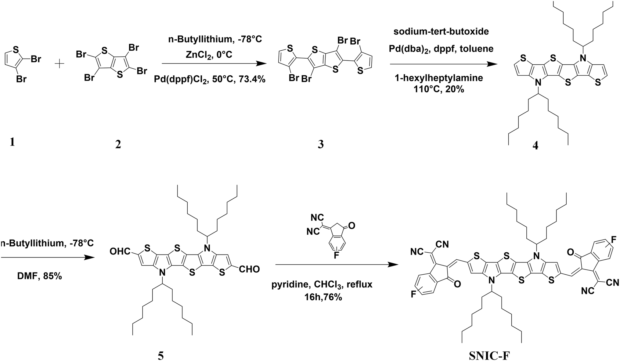
The synthetic route for SNIC-F, which was obtained in four steps, is depicted in Scheme 1. The building block of 3,6-dibromo-2,5-bis(3-bromothien-2-yl)thieno[3,2-b]thiophene (compound 3) was synthesized by the Pd-catalyzed coupling of metalated 2,3-dibromothiophene (compound 1) and tetrabromothieno[3,2-b]thiophene (compound 2). The tandem Buchwald–Hartwig reaction between compound 3 and 1-hexylheptyl amine gave the ring-fused S,N-heterohexacene compound 4. Subsequently, compound 4 was converted into its corresponding dialdehyde compound 5 by lithiation with n-butyllithium, followed by quenching with dimethylformamide (DMF). Finally, the Knoevenagel condensation reaction was conducted between compound 5 and INIC-F to produce SNIC-F in high yield. The detailed synthesis processes are given in ESI.† All of these new compounds were fully characterized by nuclear magnetic resonance (NMR), (1H, 13C) and mass spectrometry, as shown in Fig. S1–S7.†
 |
| | Scheme 1 Synthetic route of SNIC-F. | |
2.2 Optical and electrochemical properties
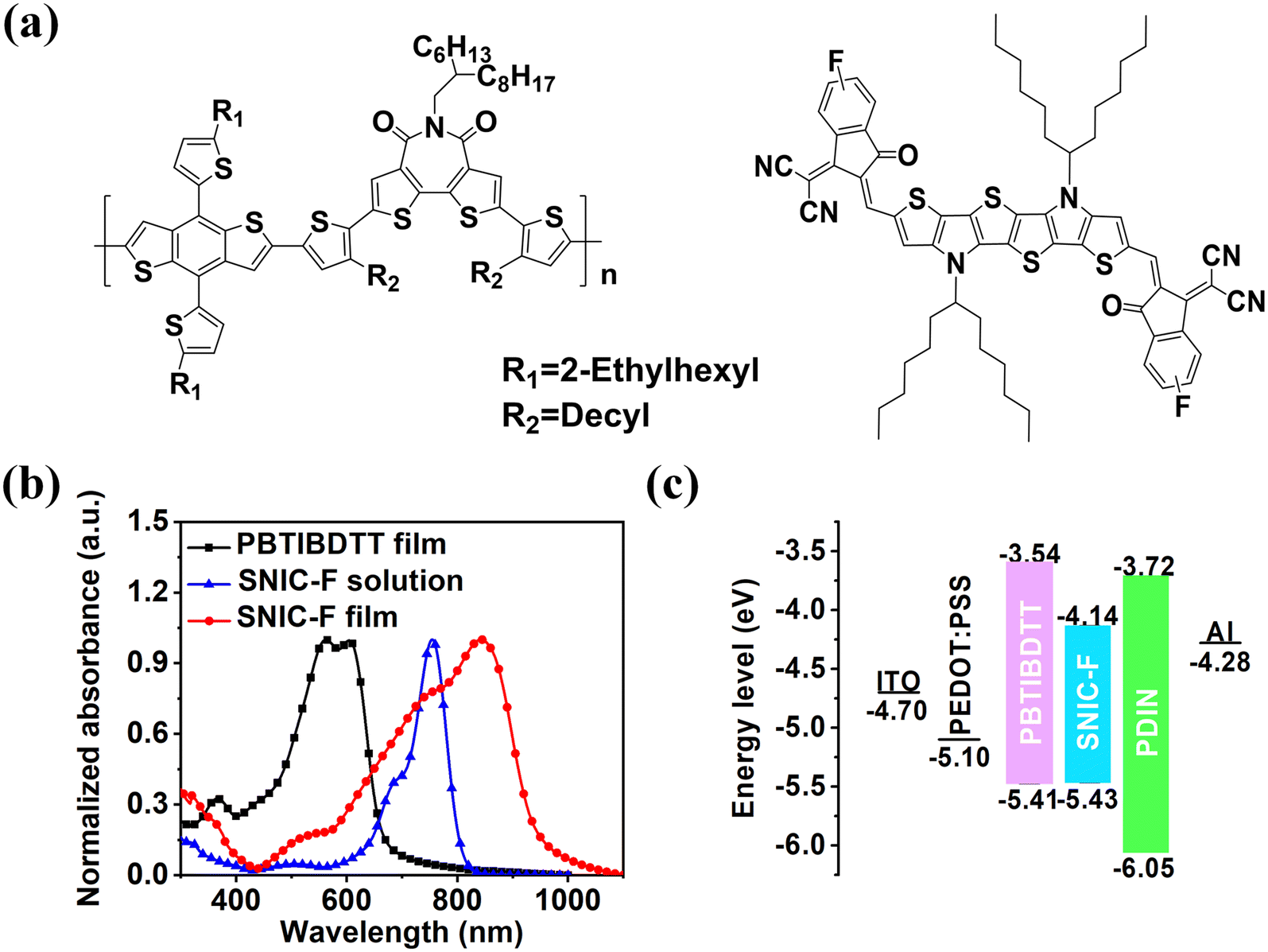
The chemical structures of PBTIBDTT and SNIC-F are given in Fig. 1a. The light absorption properties of donor PBTIBDTT and acceptor SNIC-F were evaluated by ultraviolet-visible-NIR (UV-vis-NIR) spectrophotometry. The absorption spectra of SNIC-F in chloroform solution and film are presented in Fig. 1b. In the dilute chloroform solution, a strong absorption peak from 600 nm to 800 nm was observed, along with a high extinction coefficient of 2.58 × 10⁵ M−1 cm−1. However, the thin film of SNIC-F showed an obviously broadened absorption peak from 500 nm to 940 nm. Furthermore, the film absorption spectrum displayed a red shift of about 90 nm relative to the chloroform solution. These phenomena indicated π–π stacking interactions in the solid state. The optical band gap of SNIC-F was also calculated as 1.32 eV, which was conductive to the absorption of sunlight in near-infrared region. Moreover, the combination of SNIC-F and PBTIBDTT provided a rather broad absorption in the range of 400–940 nm, which is desirable for an enhanced light harvest so as to increase Jsc.
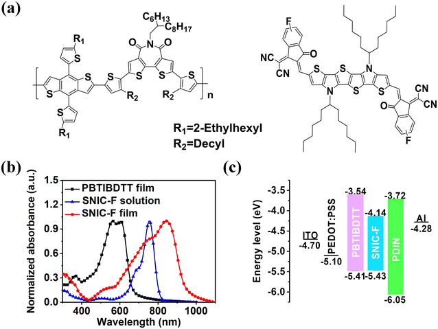 |
| | Fig. 1 (a) Chemical structures and (b) absorption spectra of PBTIBDTT and SNIC-F. (c) Energy levels of the materials in the device. | |
In order to obtain the information of the HOMO and LUMO energy levels of SNIC-F and PBTIBDTT, cyclic voltammetry was used to measure the reduction potentials and oxidation potentials. The CV curves are given in Fig. S8.† The HOMO energy levels of SNIC-F and PBTIBDTT were calculated as −5.43 eV and −5.41 eV through the corresponding onsets of the oxidation peaks. The LUMO energy levels of SNIC-F and PBTIBDTT were calculated to be −4.14 eV and −3.54 eV, respectively, according to the CV results and the optical band gaps. The column charts of the energy levels are shown in Fig. 1c. The HOMO difference between SNIC-F and PBTIBDTT was only 0.02 eV, which is much smaller than the generally empirical threshold value of 0.3 eV for effective exciton dissociation to overcome the binding energy. Despite all this, the charge transport from the SNIC-F to PBTIBDTT was also highly efficient in the PBTIBDTT:SNIC-F device. Significantly, such small HOMO offset was instrumental in obtaining a high Voc for OSCs.
2.3 Photovoltaic properties
In order to study the photovoltaic performance of the device based on PBTIBDTT:SNIC-F, the devices were prepared using the configuration of ITO/PEDOT:PSS/PBTIBDTT:SNIC-F/PDIN (N,N′-bis(propylenedimethylamine)-3,4:9,10-perylenediimide)/Al. The detailed optimization parameters of the PBTIBDTT:SNIC-F devices are provided in Tables S1–S3.† The optimal mass ratio of the donor to acceptor was optimized as 1:0.8, and its PCE was only 5.08% with a Voc of 0.81 V, an extremely low Jsc of 9.95 mA cm−2 and a FF of 0.63 before introducing the solvent additive. The extremely low Jsc resulted in a low PCE of the device without any treatment. The low Jsc demonstrated that the SNIC-F molecules might not form ideal π–π stacking in the blend film. To improve this situation, the solvent additive 1-chloronaphthalene (1-CN) was added to optimize the device.46 As shown in Table S2,† the introduction of 1-CN greatly improved the Jsc and PCE of the devices. When the content of 1-CN was 0.5%, the device showed the highest PCE of 11.25% with a Voc of 0.83 V, a remarkably improved Jsc of 19.64 mA cm−2 and a slight enhanced FF of 0.69. The external quantum efficiency (EQE) curves of the devices are given in Fig. 2b. Because of the complementary absorption of PBTIBDTT and SNIC-F, all devices showed a broad photocurrent response in the range of 300–940 nm. For the device without an additive, the EQE values were relatively low in the whole response range. However, after adding 0.5% 1-CN, the EQE values were greatly improved in the whole response range, and the maximum EQE value was 65% at 520 nm. The growth of the EQE values could greatly boost the Jsc of the device, which is in accordance with the variation trend of Jsc. In addition, the values of Jsc calculated from the EQE spectra were 9.53 mA cm−2 and 18.66 mA cm−2 for the device processed without and with 1-CN as an additive, respectively, which gave an error of only 5%. Moreover, the devices optimized by 0.5% 1-CN at different film thicknesses were prepared to investigate the sensitivity of PCEs to the film thickness. As shown in Fig. 2c, the PCEs of the optimal device still remained above 9.2% when the active layer film thicknesses were between 100 nm and 250 nm, which were attributed to the high carrier mobility of the active layers. These results showed that our work provided a possibility for solution processing of large area OSCs.
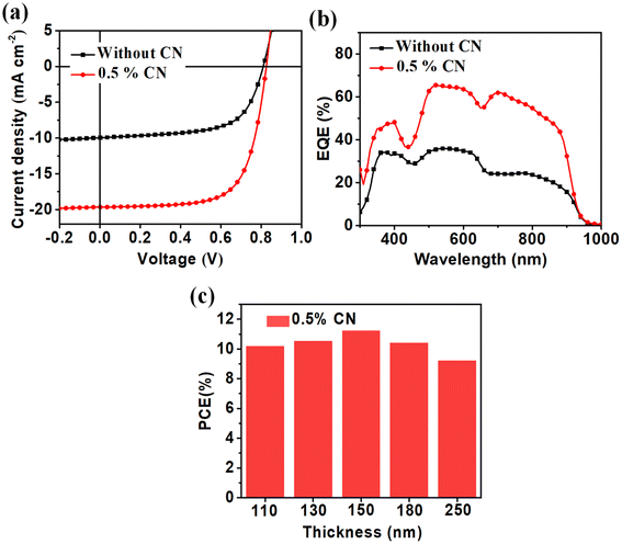 |
| | Fig. 2 (a) J–V curves and (b) corresponding EQE curves of the PBTIBDTT:SNIC-F device. (c) PCE versus the active-layer thickness. | |
2.4 Charge transport properties
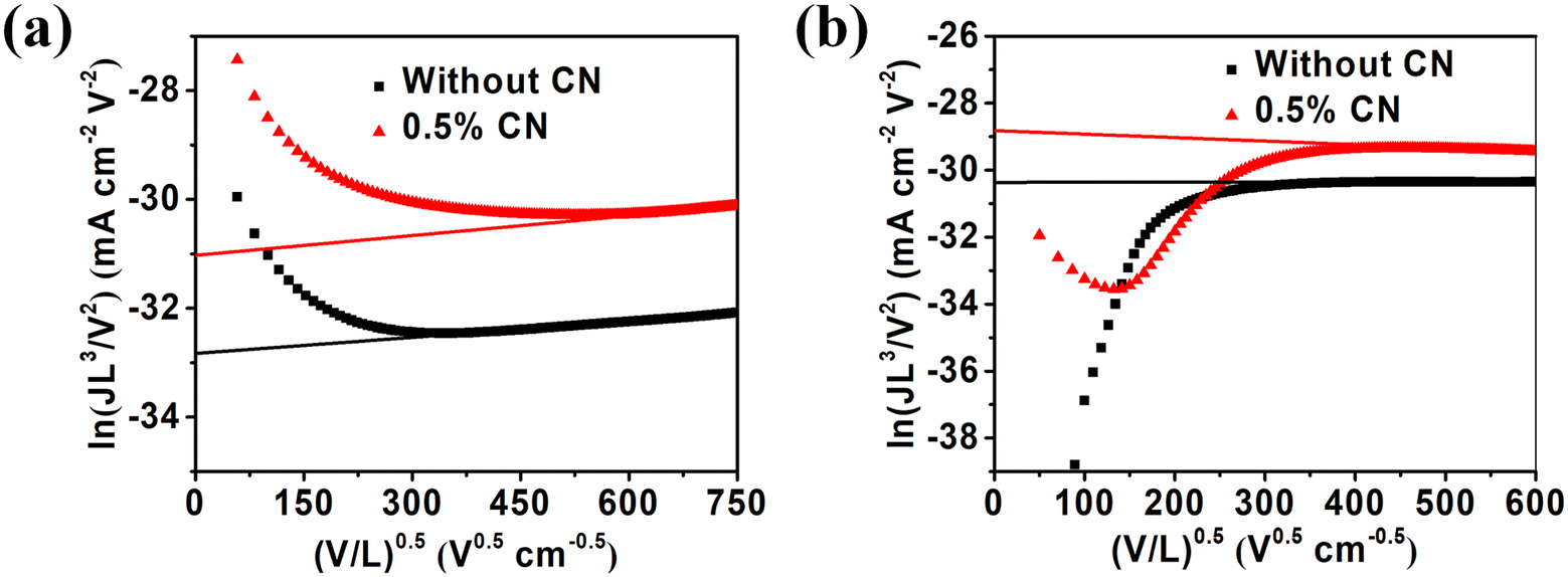
In order to study the influence of the solvent additive (1-CN) on the carrier mobility, the hole (μh) and electron (μe) mobilities of pure films and blend films based on PBTIBDTT:SNIC-F were measured by space-charge limited current (SCLC) method using a hole/electron-only device with the device structures of ITO/PEDOT:PSS/active layer/Au and ITO/ZnO/active layer/PDIN/Al, respectively. The J–V curves of these devices are shown in Fig. S9† and 3, and the corresponding data are summarized in Tables 1 and S4,† respectively. The μe of the pure SNIC-F film was calculated as 9.14 × 10⁻⁵ cm2 V−1 s−1. However, the blend film processed without 1-CN exhibited a very low μe of 1.78 × 10⁻⁵ cm2 V−1 s−1. This is probably because the crystallinity of SNIC-F is disrupted by PBTIBDTT in the blend film, which is not conducive to the charge transport. The relatively low electron mobility led to serious exciton recombination, and thus reduced the PCE of the device without 1-CN treatment. In addition, the μh of the device without 1-CN treatment was only 2.16 × 10⁻⁴ cm2 V−1 s−1. Meanwhile, for the device processed with 0.5% 1-CN, the μh increased to 1.02 × 10⁻³ cm2 V−1 s−1 and 1.18 × 10⁻⁴ cm2 V−1 s−1, respectively, and the device gave more balanced hole and electron mobilities with a μh/μe ratio of 8.6. The relatively high and more balanced hole and electron mobilities were beneficial to reducing the exciton recombination, thus improving the Jsc and FF. In order to further study the potential mechanism of improving the performance of the 1-CN processing device, the relation curves between the photocurrent density (Jph) and the effective voltage (Veff) of the devices processed with/without 1-CN were plotted, as shown in Fig. S10.† In general, Jph is defined as Jph = JL − JD, where JL, JD are the current densities under illumination and in the dark, respectively. Veff can be obtained as Veff = Vo − Va, where Vo is the voltage at which Jph = 0 and Va is the applied voltage.47 The exciton dissociation probability, Pdiss, is determined by normalized Jph at the saturated current density under short circuit condition. The corresponding parameters are summarized in Table 2. In the device without 1-CN treatment, the Pdiss was calculated to be 90.9%. The Pdiss value was calculated to be 98.0% for the device processed with 0.5% 1-CN. The higher Pdiss for the device processed with 0.5% 1-CN showed that the introduction of 1-CN reduced the geminate recombination of the device and then enhanced the Jsc, FF and PCE, which was consistent with the mobilities results.
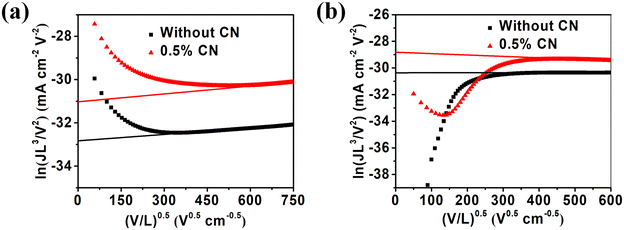 |
| | Fig. 3 J–V characteristics in the dark of (a) electron-only devices and (b) hole-only devices based on PBTIBDTT:SNIC-F without or with 0.5% 1-CN. | |
Table 1 The properties of SNIC-F and PBTIBDTT
| Compound |
λmax (nm) |
Eg (eV) |
ε (M−1 cm−1) |
HOMO (eV) |
LUMO (eV) |
μe (cm2 V−1 s−1) |
μh (cm2 V−1 s−1) |
| Solution |
Film |
| SNIC-F |
755 |
849 |
1.32 |
2.58 × 10⁵ |
−5.43 |
−4.14 |
9.14 × 10⁻⁵ |
— |
| PBTIBDTT |
603 |
604 |
1.87 |
7.94 × 10⁴ |
−5.41 |
−3.54 |
— |
8.26 × 10⁻⁴ |
Table 2 Device data of OSCs based on PBTIBDTT:SNIC-F (1:0.8, w/w)
| Additive 1-CN |
Voc (V) |
Jsc (mA cm−2) |
FF |
PCE (best)a (%) |
Calc. Jsc (mA cm−2) |
Jph (mA cm−2) |
Pdiss (%) |
| Average PCEs and standard deviations were obtained from eight devices. |
| None |
0.80 ± 0.01 |
9.62 ± 0.40 |
0.64 ± 0.02 |
4.86 ± 0.11 (5.08) |
9.53 |
10.95 |
90.9 |
| 0.5% |
0.83 ± 0.01 |
19.33 ± 0.33 |
0.69 ± 0.01 |
11.05 ± 0.12 (11.25) |
18.66 |
20.03 |
98.0 |
2.5 Crystallinity behaviors
To understand the reason for the device PCE improvement after adding 1-CN, 2D grazing-incidence wide-angle X-ray scattering (2D GIWAXS) was used to explore the crystalline structure of pure films and the blend films without and with 1-CN treatment. The crystallinity behaviors of pure PBTIBDTT and SNIC-F were firstly studied, as shown in Fig. 4. In the PBTIBDTT film, the (100) diffraction peak at qz ≈ 2.8 nm−1 [d(100) = 2.24 nm] and (010) signal peak at q ≈ 17.5 nm−1 [d(010) = 0.36 nm] in the out-of-plane (OOP) direction could be observed, which indicated that PBTIBDTT can form a π-stacking structure parallel to the substrate in the thin film. It can also be clearly seen that the SNIC-F film showed many strong diffraction signal peaks, suggesting that SNIC-F had strong crystallinity in the pure film. The 2D GIWAXS images and corresponding line profiles of the blend films are displayed in Fig. 5. In the blend film without 1-CN treatment, the weak (100) and (010) diffraction peaks in the OOP direction were observed. However, these signal peaks belonged to PBTIBDTT, and no obvious SNIC-F diffraction peak in the blend film in either OOP direction or in-plane (IP) direction was found. These results showed that SNIC-F gave an amorphous structure in the blend film without 1-CN treatment. The amorphous structure of SNIC-F would reduce the electron mobility of the blend film, which agreed well with the extremely low electron mobility of the blend film without 1-CN treatment. When 0.5% 1-CN was added as a solvent additive to optimize the blend film, an evident diffraction peak for the π–π stacking at qz ≈ 17.5 nm [d(010) = 0.36 nm] in the OOP direction was observed. This π–π stacking peak might be contributed by PBTIBDTT and SNIC-F due to the serious overlap of the π–π stacking peaks of PBTIBDTT and SNIC-F. In addition, a new diffraction signal peak at qz ≈ 6.37 nm [d(010) = 0.99 nm] in the OOP direction, which belonged to SNIC-F, was found in the blend film with 1-CN treatment. The enhancement of the π–π stacking peak and the appearance of a new diffraction peak indicated that 1-CN could promote the crystallinity of SNIC-F in the blend film. To further verify the variation of crystallinity of SNIC-F in the blend films, the absorption spectra of both blend films were obtained and normalized with the absorption peak of PBTIBDTT within 550–560 nm. As shown in Fig. 5d, the longer wavelength absorption shoulder of SNIC-F showed enhanced absorption intensity and was significantly redshifted by 20 nm. As is well known, the longer wavelength absorption shoulder of the conjugated molecule is contributed by the π–π interaction of the molecular conjugated backbones. Therefore, the enhanced and red-shifted long wavelength absorption shoulder peak signified that the addition of 1-CN could significantly improve the π–π stacking for SNIC-F in the blend film, leading to more orderly SNIC-F molecules. Combined with 2D GIWAXS and absorption spectra results, it was found that 1-CN could promote the crystallization of SNIC-F in the blend film, which could greatly improve the electronic mobility of OSCs, and thereby enhance the Jsc, FF and PCE of the device.
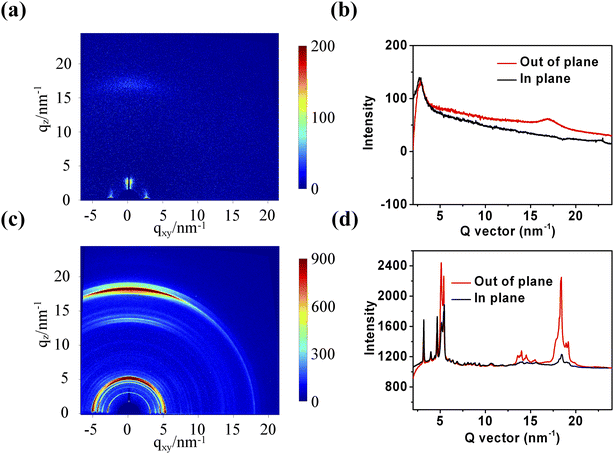 |
| | Fig. 4 The 2D GIWAXS images of (a) pure PBTIBDTT, (c) pure SNIC-F, and out-of-plane/in-plane X-ray profiles of (b) pure PBTIBDTT, (d) pure SNIC-F. | |
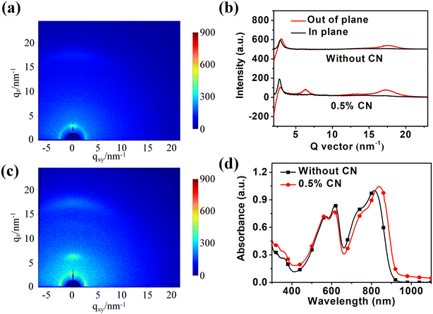 |
| | Fig. 5 The 2D GIWAXS images of PBTIBDTT:SNIC-F (a) without and (c) with 0.5% 1-CN. (b) 1D out-of-plane and in-plane X-ray profiles extracted from the 2D GIWAXS patterns. (d) The absorption spectra of the blend films with/without 1-CN. | |
2.6 Surface morphology study
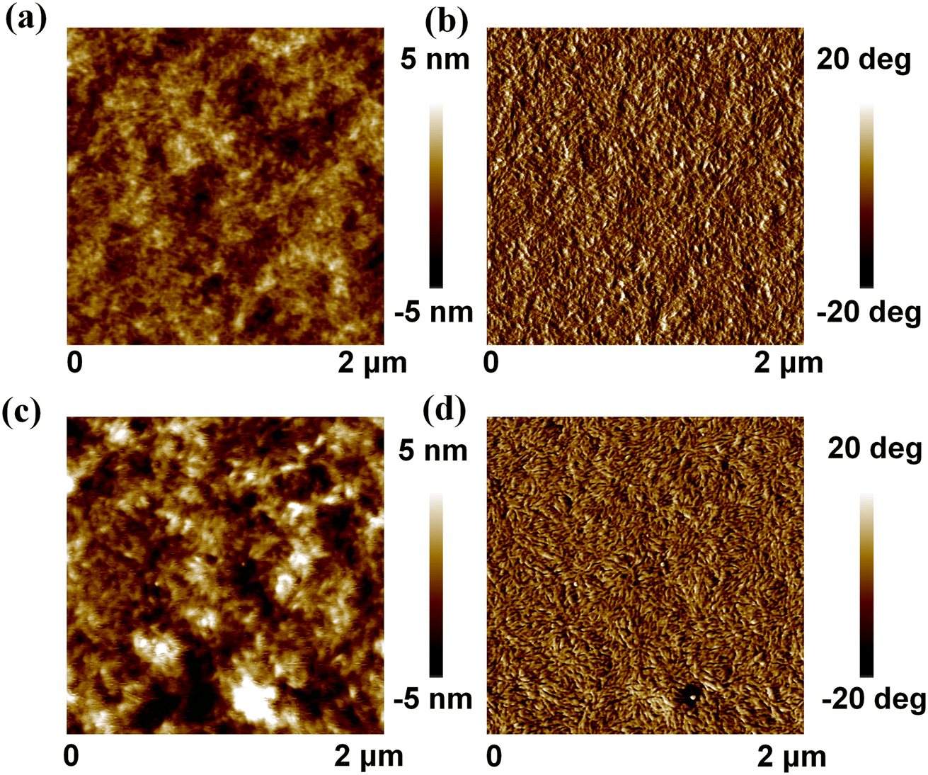
In order to further understand the effect of 1-CN on the morphology of the PBTIBDTT:SNIC-F blend films, atomic force microscopy (AFM) was used to evaluate the surface morphology of the blend films. The height and phase images of the blend films are given in Fig. 6. It can be seen from Fig. 6a and b that the blend film without 1-CN treatment displayed a uniform surface, and the value of the root mean square (RMS) roughness was only 1.26 nm. However, after the blend film was treated by 0.5% 1-CN, the surface morphology with a large domain size was observed, and the value of the RMS roughness increased to 1.73 nm. More importantly, the nanofiber structure could be observed in the blend film with 0.5% 1-CN treatment, which showed that the introduction of 1-CN could induce the crystallinity improvement in the donor and/or acceptor. The improved crystallinity of SNIC-F was also proved by XRD result. Hence, these results indicated that the solvent additive 1-CN could improve the crystallinity of SNIC-F, which could explain the enhanced electron mobility, π–π stacking and thus the higher FF and Jsc.
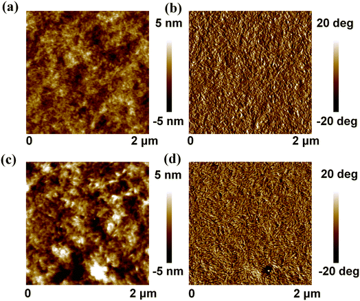 |
| | Fig. 6 AFM topography (a and c) and phase (b and d) images of the blend films processed without (a and b) and with 0.5% 1-CN (c and d) as an additive. | |
3 Conclusion
In conclusion, a novel DTP-based NFSMA, SNIC-F, was developed and studied. SNIC-F showed a low optical band gap of 1.32 eV due to the strong intramolecular charge transfer effect. When the D–A type copolymer PBTIBDTT was chosen as the donor, the HOMO energy offset between PBTIBDTT and SNIC-F was only 0.02 eV, which was far less than the empirical value of 0.3 eV. Despite the minimal HOMO energy offset, the device optimized by 0.5%-1-CN exhibited a high PCE of 11.25%, along with a high Jsc of 19.64 mA cm−2, a Voc of 0.83 V and a FF of 0.69. In addition, this device could maintain a PCE above 9.2% as the active layer thickness increased to 250 nm. Our work showed that synthesizing the DTP-based narrow band gap NFSMA and matching it with a polymer donor with minimal HOMO offset is an efficient method for obtaining high performance OSCs based on NFSMAs.
Conflicts of interest
There are no conflicts to declare.
Acknowledgements
This work was financially supported by the Jiangmen Basic and Theoretical Scientific Research Science and Technology Plan Project (2020JC01022), and Key Project of Jiangmen Basic and Applied Basic Research (2021030103700007392).
References
- H. Yao, Y. Cui, D. Qian, C. S. Ponseca Jr, A. Honarfar, Y. Xu, J. Xin, Z. Chen, L. Hong, B. Gao, R. Yu, Y. Zu, W. Ma, P. Chabera, T. Pullerits, A. Yartsev, F. Gao and J. Hou, J. Am. Chem. Soc., 2019, 141, 7743–7750 CrossRef CAS PubMed.
- Y. Xin, G. Zeng, J. Zhang, X. Zhao and X. Yang, J. Mater. Chem. A, 2018, 6, 9561–9568 RSC.
- C. Sun, F. Pan, H. Bin, J. Zhang, L. Xue, B. Qiu, Z. Wei, Z.-G. Zhang and Y. Li, Nat. Commun., 2018, 9, 743 CrossRef PubMed.
- X. Chen, G. Xu, G. Zeng, H. Gu, H. Chen, H. Xu, H. Yao, Y. Li, J. Hou and Y. Li, Adv. Mater., 2020, 32, 1908478 CrossRef CAS PubMed.
- X. Chen, T. Lai, T. Shi, X. Peng and S. Zhang, IEEE J. Photovolt., 2022, 12, 316–321 Search PubMed.
- B. Kan, M. Li, Q. Zhang, F. Liu, X. Wan, Y. Wang, W. Ni, G. Long, X. Yang, H. Feng, Y. Zuo, M. Zhang, F. Huang, Y. Cao, T. P. Russell and Y. Chen, J. Am. Chem. Soc., 2015, 137, 3886–3893 CrossRef CAS PubMed.
- D. Yang, T. Zhang, X. Zhao, G. Zeng, Z. Li, Y. Tian, F. He, J. Zhang and X. Yang, Polym. Chem., 2016, 7, 5366–5374 RSC.
- M. Cao, L. Wang, H. Gao, H. Jiang and H. Song, New J. Chem., 2023, 47, 1797–1807 RSC.
- Y. Duan, X. Xu, H. Yan, W. Wu, Z. Li and Q. Peng, Adv. Mater., 2017, 29, 1605115 CrossRef PubMed.
- M. Rani, N. M. A. Hadia, A. M. Shawky, R. F. Mehmood, S. Hameed, S. Zahid, J. Iqbal, N. S. Alatawi, A. Ahmed and R. A. Khera, RSC Adv., 2023, 13, 1640–1658 RSC.
- G. Zeng, J. Ouyang, Y. Xin, X. Zhao and X. Yang, J. Mater. Chem. C, 2018, 6, 13211–13217 RSC.
- J. Gao, N. Yu, Z. Chen, Y. Wei, C. Li, T. Liu, X. Gu, J. Zhang, Z. Wei, Z. Tang, X. Hao, F. Zhang, X. Zhang and H. Huang, Adv. Sci., 2022, 9, 2203606 CrossRef CAS PubMed.
- R. Sun, Y. Wu, X. Yang, Y. Gao, Z. Chen, K. Li, J. Qiao, T. Wang, J. Guo, C. Liu, X. Hao, H. Zhu and J. Min, Adv. Mater., 2022, 34, 2110147 CrossRef CAS PubMed.
- L. Zhu, M. Zhang, J. Xu, C. Li, J. Yan, G. Zhou, W. Zhong, T. Hao, J. Song, X. Xue, Z. Zhou, R. Zeng, H. Zhu, C.-C. Chen, R. C. I. MacKenzie, Y. Zou, J. Nelson, Y. Zhang, Y. Sun and F. Liu, Nat. Mater., 2022, 21, 656–663 CrossRef CAS PubMed.
- Y. Lin, J. Wang, Z.-G. Zhang, H. Bai, Y. Li, D. Zhu and X. Zhan, Adv. Mater., 2015, 27, 1170–1174 CrossRef CAS PubMed.
- J. Hou, O. Inganäs, R. H. Friend and F. Gao, Nat. Mater., 2018, 17, 119–128 CrossRef CAS PubMed.
- C. Li, J. Song, Y. Cai, G. Han, W. Zheng, Y. Yi, H. S. Ryu, H. Y. Woo and Y. Sun, J. Energy Chem., 2020, 40, 144–150 CrossRef.
- X. Liu, Y. Xie, X. Cai, Y. Li, H. Wu, S.-J. Su and Y. Cao, RSC Adv., 2015, 5, 107566–107574 RSC.
- J. Song, C. Li, L. Ye, C. Koh, Y. Cai, D. Wei, H. Y. Woo and Y. Sun, J. Mater. Chem. A, 2018, 6, 18847–18852 RSC.
- Y. Xin, J. Liang, Y. Zhong, T. Liang, C. Zhang and X. He, Dyes Pigm., 2021, 195, 109661 CrossRef CAS.
- C. Yan, S. Barlow, Z. Wang, H. Yan, A. K. Y. Jen, S. R. Marder and X. Zhan, Nat. Rev. Mater., 2018, 3, 18003 CrossRef CAS.
- S. Feng, C. e. Zhang, Y. Liu, Z. Bi, Z. Zhang, X. Xu, W. Ma and Z. Bo, Adv. Mater., 2017, 29, 1703527 CrossRef PubMed.
- Y. Guo, L. Zhu, R. Duan, G. Han and Y. Yi, Chem.–Eur. J., 2023, 29, e202203356 CrossRef CAS PubMed.
- M. Li, Z. Li, G. Song, C. Jiang, X. Chen, J. Wang, Y. Yang, X. Wan, C. Li and Y. Chen, J. Mater. Chem. C, 2023, 11, 1155–1164 RSC.
- X. Li, H. Huang, Z. Peng, C. Sun, D. Yang, J. Zhou, A. Liebman-Pelaez, C. Zhu, Z.-G. Zhang, Z. Zhang, Z. Xie, H. Ade and Y. Li, J. Mater. Chem. A, 2018, 6, 15933–15941 RSC.
- Y. Ma, R. Sun, Z. Chen, S. Zhang, D. Cai, S. Wan, W. Lin, S.-Q. Zhang, Q. Tu, W. Ma, J. Min, X. Hao and Q. Zheng, Nano Energy, 2023, 107, 108116 CrossRef CAS.
- G. Zeng, Y. Xin, B. Zhang, J. Ouyang, X. Zhao and X. Yang, Sol. RRL, 2020, 4, 2000234 CrossRef CAS.
- J. Cao, S. Qu, J. Yu, Z. Zhang, R. Geng, L. Yang, H. Wang, F. Du and W. Tang, Mater. Chem. Front., 2020, 4, 924–932 RSC.
- Y. Chen, T. Liu, H. Hu, T. Ma, J. Y. L. Lai, J. Zhang, H. Ade and H. Yan, Adv. Energy Mater., 2018, 8, 1801203 CrossRef.
- X. Ke, L. Meng, X. Wan, Y. Cai, H.-H. Gao, Y.-Q.-Q. Yi, Z. Guo, H. Zhang, C. Li and Y. Chen, Nano Energy, 2020, 75, 104988 CrossRef CAS.
- Z. Liang, X. Cheng, Y. Jiang, J. Yu, X. Xu, Z. Peng, L. Bu, Y. Zhang, Z. Tang, M. Li, L. Ye and Y. Geng, ACS Appl. Mater. Interfaces, 2021, 13, 61487–61495 CrossRef CAS PubMed.
- W. Wang, C. Yan, T.-K. Lau, J. Wang, K. Liu, Y. Fan, X. Lu and X. Zhan, Adv. Mater., 2017, 29, 1701308 CrossRef PubMed.
- H. Yao, Y. Cui, R. Yu, B. Gao, H. Zhang and J. Hou, Angew. Chem., Int. Ed., 2017, 56, 3045–3049 CrossRef CAS PubMed.
- J. Lee, S.-J. Ko, M. Seifrid, H. Lee, C. McDowell, B. R. Luginbuhl, A. Karki, K. Cho, T.-Q. Nguyen and G. C. Bazan, Adv. Energy Mater., 2018, 8, 1801209 CrossRef.
- J. Cao, F. Du, L. Yang and W. Tang, J. Mater. Chem. A, 2020, 8, 22572–22592 RSC.
- Y.-C. Lin, N.-Z. She, C.-H. Chen, A. Yabushita, H. Lin, M.-H. Li, B. Chang, T.-F. Hsueh, B.-S. Tsai, P.-T. Chen, Y. Yang and K.-H. Wei, ACS Appl. Mater. Interfaces, 2022, 14, 37990–38003 CrossRef CAS PubMed.
- A. Mishra, M. L. Keshtov, A. Looser, R. Singhal, M. Stolte, F. Würthner, P. Bäuerle and G. D. Sharma, J. Mater. Chem. A, 2017, 5, 14887–14897 RSC.
- Y. Geng, A. Tang, K. Tajima, Q. Zeng and E. Zhou, J. Mater. Chem. A, 2019, 7, 64–96 RSC.
- C. Huang, X. Liao, K. Gao, L. Zuo, F. Lin, X. Shi, C.-Z. Li, H. Liu, X. Li, F. Liu, Y. Chen, H. Chen and A. K. Y. Jen, Chem. Mater., 2018, 30, 5429–5434 CrossRef CAS.
- X. Chen, H. Liu, L. Xia, T. Hayat, A. Alsaedi and Z. a. Tan, Chem. Commun., 2019, 55, 7057–7060 RSC.
- S. Ma, S. Wu, J. Zhang, Y. Song, H. Tang, K. Zhang, F. Huang and Y. Cao, ACS Appl. Mater. Interfaces, 2020, 12, 51776–51784 CrossRef CAS PubMed.
- S. Li, L. Zhan, C. Sun, H. Zhu, G. Zhou, W. Yang, M. Shi, C.-Z. Li, J. Hou, Y. Li and H. Chen, J. Am. Chem. Soc., 2019, 141, 3073–3082 CrossRef CAS PubMed.
- X. Liu, Y. Li, K. Ding and S. Forrest, Phys. Rev. Appl., 2019, 11, 024060 CrossRef CAS.
- Y. Liu, L. Zuo, X. Shi, A. K. Y. Jen and D. S. Ginger, ACS Energy Lett., 2018, 3, 2396–2403 CrossRef CAS.
- Y. Xu, H. Yao, L. Ma, L. Hong, J. Li, Q. Liao, Y. Zu, J. Wang, M. Gao, L. Ye and J. Hou, Angew. Chem., Int. Ed., 2020, 59, 9004–9010 CrossRef CAS PubMed.
- T. Ye, S. Jin, R. Singh, M. Kumar, W. Chen, D. Wang, X. Zhang, W. Li and D. He, Sol. Energy, 2020, 201, 927–934 CrossRef CAS.
- C. Xu, K. Jin, Z. Xiao, Z. Zhao, X. Ma, X. Wang, J. Li, W. Xu, S. Zhang, L. Ding and F. Zhang, Adv. Funct. Mater., 2021, 31, 2107934 CrossRef CAS.
|
| This journal is © The Royal Society of Chemistry 2023 |
Click here to see how this site uses Cookies. View our privacy policy here. 
 Open Access Article
 This Open Access Article is licensed under a Creative Commons Attribution-Non Commercial 3.0 Unported Licence
 *b and
Shengdong Zhanga
*b and
Shengdong Zhanga