DOI:
10.1039/D3RA00791J
(Paper)
RSC Adv., 2023,
13, 11324-11336
Theoretical insights into the amplified optical gain of hexagonal germanium by strain engineering†
Received
6th February 2023
, Accepted 17th March 2023
First published on 11th April 2023
Abstract
Strain engineering is a versatile technique used to tune the electronic and optical attributes of a semiconductor. A proper degree of strain can induce the optimum amount of gain necessary for light-emitting applications. Particularly, photonic integrated chips require an efficient light-emitting material that can be easily assimilated into complementary metal-oxide semiconductor (CMOS) technology. Germanium falls in the same group of the periodic table as silicon, and thus, it completely complies with Si technology. Hence, we investigated extensively the electronic and optical properties of hexagonal germanium for both compressive and tensile strains using density functional theory. The electronic bandstructure, dielectric function, absorption, and reflectivity were calculated by employing a modified Becke–Johnson (mBJ) potential including spin–orbit coupling for uniaxial strains ±0.5–5%. We calculated the effective masses at various symmetry points and determined other band parameters, including the crystal field splitting and spin–orbit splitting energies. The partial, projected, and total density of states were discussed in great depth to unveil the characteristics of the energy states that take part in optical transitions. Finally, the optical gain for the semiconductor was calculated as a function of strain. After the band inversion phenomenon, hex-Ge generates a huge increase in the amplification and bandwidth of optical gain. This results from the increased electron concentration in Γ−7c state and enhanced momentum matrix between the p-character valence states and sp-hybridized states of the conduction band. Conduction band to light hole recombination is observed to improve the light emission to a great extent.
1. Introduction
In recent years, the integration of an efficient optical device into complementary metal-oxide semiconductor (CMOS) technology has gained high technological interest.1 Perhaps, this could possibly address the growing high-data transmissions and high-speed interconnections for signal processing and high-performance computing.2 However, photonic integration for microelectronics and optical communication technologies requires on-chip laser materials with efficient emitting power and compatibility with CMOS technology.3 Under the ambient conditions, cubic diamond structure (space group Fd![[3 with combining macron]](https://www.rsc.org/images/entities/char_0033_0304.gif) m) of silicon has an indirect band gap of 1.1 eV; therefore, it does not emit light efficiently.4 Even the material remains indirect if the structure is changed to hexagonal with space group P63/mmc.5 Germanium, belonging to the same group, possesses a similar electronic configuration as that of silicon and so conforms to Si technology.6 Similar to Si, Ge naturally occurrs in the cubic phase and has an indirect band gap of 0.7 eV.7 However, hexagonal Ge (hex-Ge) has been reported to have a direct band gap of around 0.3 eV, which lies in the mid-infrared region.8 Earliest preparation of the crystal was performed using strain-induced and low-pressure ultraviolet laser ablation methods.9,10 Surprisingly, high quality crystals of hex-Ge have been successfully grown over III–V semiconductors via crystal transfer methods and epitaxy methods.11,12 Undoubtedly, the direct nature of the bandgap has great significance for laser materials to be used as an optical source.13 In addition, other material aspects, such as wavelength tunability, allowed transitions, and radiative recombination rates, are also critical for efficient light emission and implementation in different infrared regimes.11,14 To engineer and optimize the material characteristics of the semiconductor for better harness, straining, nanostructuring, alloying, and amorphization have proved to be effective strategies.8,15 By alloying germanium with several other atoms, it has been possible to chemically tune the band structure and bring about favorable changes in the optoelectronic performance of the device structure.11,16,17 Overall, strain engineering has become a highly promising method for achieving the optimal band gap and enhancing gain in emission. For instance, the electronic properties of strained cubic Ge thin films have been investigated both theoretically and experimentally.18 Similarly, the transport and optical properties were studied for lasing action and interband absorption.19 Tensile strain has been extensively studied in germanium for its potential to engineer the bandgap and improve the efficiency of light emission.20–22 Tahini et al. showed that moderate uniaxial strain along the [111] direction transforms Ge into a direct bandgap material.23 Similarly, tensile strain induces a direct bandgap in (100) and (110) strained GeSn, while compressive strain has a positive effect on (111) orientation.24 Moreover, Ge nanowires have been investigated to explore the effect of uniaxial strain on the bandgap and effective masses.25 Lately, the electronic, and optical properties of hex-Ge have been accurately explored using both the hybrid Heyd–Scuseria–Ernzerhof (HSE) functional and modified Becke–Johnson exchange potential (MBJ).8 Later, Suckert et al. also studied the effects of hydrostatic pressure, biaxial strain, and uniaxial strain.14 Likewise, Belabbes et al. evaluated the interband transition energies for uniaxially strained lonsdaleite germanium and Ge–Si alloy.26 However, a thorough understanding of the structure–property relationship of uniaxially strained hexagonal germanium is essential to effectively comprehend the potential characteristics of light-emitting materials.
m) of silicon has an indirect band gap of 1.1 eV; therefore, it does not emit light efficiently.4 Even the material remains indirect if the structure is changed to hexagonal with space group P63/mmc.5 Germanium, belonging to the same group, possesses a similar electronic configuration as that of silicon and so conforms to Si technology.6 Similar to Si, Ge naturally occurrs in the cubic phase and has an indirect band gap of 0.7 eV.7 However, hexagonal Ge (hex-Ge) has been reported to have a direct band gap of around 0.3 eV, which lies in the mid-infrared region.8 Earliest preparation of the crystal was performed using strain-induced and low-pressure ultraviolet laser ablation methods.9,10 Surprisingly, high quality crystals of hex-Ge have been successfully grown over III–V semiconductors via crystal transfer methods and epitaxy methods.11,12 Undoubtedly, the direct nature of the bandgap has great significance for laser materials to be used as an optical source.13 In addition, other material aspects, such as wavelength tunability, allowed transitions, and radiative recombination rates, are also critical for efficient light emission and implementation in different infrared regimes.11,14 To engineer and optimize the material characteristics of the semiconductor for better harness, straining, nanostructuring, alloying, and amorphization have proved to be effective strategies.8,15 By alloying germanium with several other atoms, it has been possible to chemically tune the band structure and bring about favorable changes in the optoelectronic performance of the device structure.11,16,17 Overall, strain engineering has become a highly promising method for achieving the optimal band gap and enhancing gain in emission. For instance, the electronic properties of strained cubic Ge thin films have been investigated both theoretically and experimentally.18 Similarly, the transport and optical properties were studied for lasing action and interband absorption.19 Tensile strain has been extensively studied in germanium for its potential to engineer the bandgap and improve the efficiency of light emission.20–22 Tahini et al. showed that moderate uniaxial strain along the [111] direction transforms Ge into a direct bandgap material.23 Similarly, tensile strain induces a direct bandgap in (100) and (110) strained GeSn, while compressive strain has a positive effect on (111) orientation.24 Moreover, Ge nanowires have been investigated to explore the effect of uniaxial strain on the bandgap and effective masses.25 Lately, the electronic, and optical properties of hex-Ge have been accurately explored using both the hybrid Heyd–Scuseria–Ernzerhof (HSE) functional and modified Becke–Johnson exchange potential (MBJ).8 Later, Suckert et al. also studied the effects of hydrostatic pressure, biaxial strain, and uniaxial strain.14 Likewise, Belabbes et al. evaluated the interband transition energies for uniaxially strained lonsdaleite germanium and Ge–Si alloy.26 However, a thorough understanding of the structure–property relationship of uniaxially strained hexagonal germanium is essential to effectively comprehend the potential characteristics of light-emitting materials.
In this work, we present a systematic and thorough analysis of the electronic and optical properties of the hex-Ge under uniaxial compressive and tensile strains. The carefully optimized strained and unstrained lattice structures were used to predict the electronic and optical properties. The study of the density of states helped to understand the electronic band structure more intuitively. Under the application of strain, the variation caused in the conduction band and the valence bands are realized by means of the partial, projected, and total density of states, crystal field energies, spin–orbit splitting energies, and effective masses. The optical properties were explored using the dielectric function, absorption, and refractive index. To assess the performance of the light-emitting device, we discussed the optical gain of hex-Ge under various degrees of uniaxial strains.
2. Computational details
All the calculations were performed using the Vienna Ab initio Simulation Package (VASP), based on the plane wave method within density-functional theory (DFT).27 The projector augmented wave method was used to describe the interactions of core electrons and valence electrons with a plane-wave energy cutoff of 500 eV. The outermost electrons Ge (3d104s24p2) were treated for the expansion of wave functions. A well-converged k-point mesh of 12 × 12 × 6 Monkhorst–Pack was employed for Brillouin-zone integration. The self-consistent field equations were performed with the Gaussian smearing technique to achieve total energy convergence of 10−6 eV per atom. The pristine structure was optimized by relaxing ions, volume, and shape whereas optimized geometries for strained structures were obtained by carrying out restricted ionic relaxations on a few degrees of freedom. The conjugate-gradient algorithm was used for structural optimization to ensure that the force on each atom was less than 5 meV Å−1.
The structural and elastic properties were determined using the generalized gradient approximation (GGA) with Perdew–Burke–Ernzerhof revised for solids (PBE-sol) exchange–correlation functional, which is proved very accurate for the prediction of lonsdaleite germanium.28 In principle, the spin–orbit coupling has been reported to have no significant impact on the lattice constants, and thereby, has been neglected in structural and elastic calculations.8 Contrarily, the electronic band structures have been calculated with the modified Becke–Johnson (mBJ) potential with the incorporation of spin–orbit coupling.29 The semi-local meta-GGA functional is known to produce highly accurate band gap values for a wide range of semiconducting materials. This can be attributed to the inclusion of orbital-dependent model corrections, which are not present in standard local density approximation (LDA) or GGA functionals.30 Furthermore, the MBJ functional also does not require solving a large number of Poisson equations in contrast to hybrid functionals and Gross–Weizsäcker (GW) approximations and thus, is computationally efficient.
In this work, tensile and compressive strains were applied along the lattice c-axis and atomic coordinates were relaxed. Tensile is represented as positive (+) and compression as negative (−) strains. The uniaxial strains were implemented stepwise with magnitudes from −5% to 5%. Then, the relaxed structures were used to calculate the electronic and optical properties.
3. Results and discussion
3.1 Structural and elastic properties
In a unit cell of hex-Ge, each Ge atom is tetrahedrally bonded by other Ge atoms as shown in the conventional cell in Fig. 1(a). The crystal with the space group: 194 (P63/mmc) has an AB stacking of Ge bilayers, which is in contrast to the ABC stacking exhibited by cubic Ge.8 To check the accuracy, we calculated the lattice parameters of hex-Ge using both the standard PBE and PBE-sol functionals. Our predicted lattice parameters shown in Table 1 and calculated using PBE-sol are in excellent agreement with the experimental values.11 Moreover, the five independent elastic constants, C11, C12, C13, C44, and C66 for hex-Ge were calculated using the first principles approach and compared with the existing theoretical results in Table 2.14,31 Elastic constants and moduli decrease with compression and increase with tensile strain, consistent with strain application.
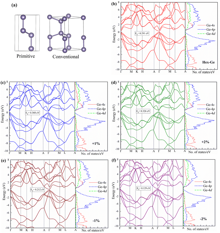 |
| | Fig. 1 (a) Unit cell of hexagonal germanium crystal as produced with VESTA package. Bandstructure and partial density of states for (b) pristine hex-Ge, under tensile strains of (c) 1%, (d) 2% and compressive strains of (e) 1%, and (f) 2%. | |
Table 1 Calculated lattice values and band gap compared with earlier reported values of hexagonal germanium
| Lattice parameters (Å) |
Band gap (eV) |
| |
This work |
Other theo. |
Expt. |
This work |
Other theo. |
Expt. |
| PBE |
PBE sol |
| Ref. 8. Ref. 14. At T = 4 K (ref. 11). At T = 300 K (ref. 11). |
| a |
4.05 |
3.99 |
3.99a, 4.00b |
3.96c |
0.291 |
0.286a, 0.298b |
0.35c, 0.28d |
| c |
6.68 |
6.59 |
6.59a, 6.56b |
6.57c |
|
|
|
Table 2 Calculated elastic constants, Cij, bulk modulus (B), shear modulus (G), Young's modulus (Y), and Poisson's ratio (σ) of unstrained and strained hex-Ge compared with earlier reported values of hexagonal germanium. The elastic constants and moduli are in the units of GPa and σ is unitless
| |
−2% |
−1% |
Hex-Ge |
+1% |
+2% |
| Ref. 14. Ref. 31. |
| C11 |
144.3 |
144.1 |
143.2, 124a, 155.6b |
141.4 |
140.0 |
| C12 |
45.4 |
42.2 |
40.4, 53.7a, 37.5b |
39.1 |
38.5 |
| C13 |
33.2 |
29.4 |
25.1, 22.8a, 27.7b |
22.0 |
19.8 |
| C33 |
176.1 |
173.4 |
168.7, 159.4a, 169.3b |
161.8 |
150.0 |
| C44 |
42.0 |
41.7 |
41.1, 39.1a, 41.1b |
40.4 |
40.2 |
| C66 |
49.5 |
51.0 |
51.4, 35.2a, 59.1b |
51.2 |
50.7 |
| B |
76.4 |
73.67 |
70.7, 67.3a, 74b |
67.9 |
65.1 |
| G |
49.4 |
50.0 |
50.1, 42a, 52.9b |
49.5 |
48.8 |
| Y |
122 |
122.4 |
121.5, 153.3a, 127.6b |
119.5 |
117.2 |
| σ |
0.23 |
0.22 |
0.21, 0.22a, 0.21b |
0.20 |
0.19 |
3.2 Electronic properties
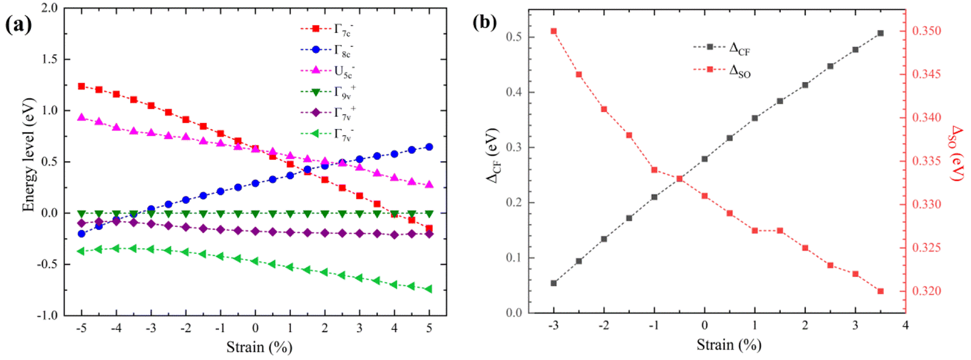
An efficient light emission is of paramount importance in any light source in light-emitting diode (LED) or lasers. This necessitates the material to have a direct band-gap nature. Essentially, the electronic band structure of the optimized hex-Ge crystal was calculated along high symmetry lines. Fig. 1(b) shows the calculated band structure of the pristine hex-Ge, indicating a direct band gap of 0.291 eV at the gamma-point. Our computed band gap values in Table 1 agree with the previous theoretical values calculated with HSE and MBJ functionals.8,14 This calculated band gap using DFT at 0 K shows a reasonable agreement with the experimental values of 0.35 eV at 4 K (a difference of 0.06 eV) and 0.28 eV at 300 K (a difference of 0.011 eV), which suggests variation rates of 17.14% and 3.93%, respectively.11 As illustrated in Fig. 1(c and d), with the increase of tensile strain, the band gap increases initially and then decreases gradually. However, we observed a monotonous decrease in the band gap with the application of compressive strain (Fig. 1(e and f)). To analyse in detail the bonding character, we calculated the partial density of states (PDOS), which shows the contribution of different orbitals of Ge. Evidently, in Fig. 1(b), the plotted PDOS for the pristine hex-Ge clearly shows that the upper portion of the valence band is dominated by Ge-4p orbitals. But the states below −5 eV are mainly composed of Ge-4s orbitals. The states in the conduction band are formed due to both Ge-4s and Ge-4p orbitals, where the former constitute the conduction band minimum, and the latter contributes to the higher energy states. Under both uniaxial tensile and compressive strains, the profile of PDOS looks similar in all the investigated materials. However, we can notice a clear alteration of the electronic characteristics in the total density of states (TDOS), as shown in Fig. 2(a and b). The edges of the conduction bands drift towards the lower energy side due to the reduction of the band gaps via uniaxial strain. It is worth mentioning that the tensile strain on hex-Ge induces a higher density of states in comparison with the compressive counterpart. Considering the conduction states within the energy range of 0–1.2 eV, the density grows nearly 1.2–1.3 times when the material is stretched along the c-axis. The factors leading to bandgap evolution and the modification of TDOS are elucidated in detail with the help of hexagonal symmetry and projected density of states. Due to the hexagonal symmetry of hex-Ge, the structure possesses a valence band comprising three non-degenerate states, Γ+9v+, Γ+7v+ and Γ+7v−.32 These are also known as heavy holes, light holes, and split-off bands, respectively. Whereas, in the conduction bands, there are two conduction states, Γ−7c and Γ−8c. Γ−7c is referred to as the bright conduction band and Γ−8c as the dark conduction band. According to group theory, for light polarization parallel to the c-axis, we have forbidden optical transition between the highest conduction state Γ+9v and lowest conduction state, Γ−8c and so, hex-Ge is referred to as a pseudo-direct semiconductor.33 Insightfully, we have illustrated in Fig. 2(c, d), S1(a and b) of the ESI,† the calculated projected band structures of the unstrained and strained structures along high symmetry points, A, Γ, M, and L.
 |
| | Fig. 2 Total density of states for (a) hex-Ge, and under tensile strains of 1%, 2%, and 3%, and (b) hex-Ge and under compressive strains of 1%, 2% and 3%. Projected band structures of (c) hex-Ge, and (d) under tensile strain of 1.5%. | |
To clearly distinguish the characteristics of the states along different directions, the weights of projections of the orbitals have been well-preserved. In pristine hex-Ge, the conduction states Γ−7c and Γ−8c are coloured with Ge-4s orbitals (red bubble) from Γ to A (A is ∥ to c-axis), whereas Γ to M (M is ⊥ to c-axis) has substantial Ge-4p character (blue bubble). Interestingly, this might be a reason for the preferential transitions for the light polarization perpendicular to the c-axis.14 Additionally, it is also reported that the p–p optical transition between the conduction band and valence band is stronger than that of s–p transition.34 On the other side, all the three valence states Γ+9V, Γ+7V+ and Γ+9V− are due to Ge-4p orbitals. Under uniaxial tensile strain, the initial rise in the band gap is caused by the shift of Γ−8c towards higher conduction energy levels. As tensile strain is applied further, Γ−7c gradually shift downwards and eventually cross the Γ−8c to become the lowest conduction state at about +1.5% strain (Fig. 2(d)). This phenomenon marks the transition of the material from pseudo-direct to direct hex-Ge. Additionally, the two energy states Γ−7c and Γ−8c, which are lying very close to each other explains the increased density of states under the tensile strain (Fig. 2(a)). The bandgap declines further with the increase of tensile strain and around 4% tensile strain, the 2H-Ge transforms into a metal, which is also, evident from the overlap of the Ge-4p and Ge-4s orbitals (Fig. S1(a) of ESI†). In essence, the band gap after the inversion of the conduction states and before the transition to metal can be harnessed effectively for wavelength tuning in photonic devices. On the other hand, compressive strain along the c-axis causes bandgap narrowing due to the downshift of the dark conduction state Γ−8c towards the valence band (Fig. S1(b) of ESI†). Γ−7c and Γ−8c drift away from each other with rising compression, reducing the density of states. Here, the band inversion does not occur, hence, the semiconductor remains pseudo-direct as before. Similar to the tensile strain, when 3.5% compressive strain is applied, the semiconductor-to-metal transition occurs. The conduction band valley between the symmetry points M and L (sometimes referred to as the U−5c state) has more s character than p. U−5c follows the trend of the Γ−7c state under tensile strain but slightly moves upward with compression relative to the heavy hole state, Γ−9v.
To study the movement of the energy states, we have plotted the energy levels as a function of strain in Fig. 3(a), keeping Γ+9V at the reference zero level. Under tensile strain, the cross-over point of the energy states, Γ−7c and Γ−8c corresponding to the pseudo-direct-to-direct transition and semiconductor-to-metal transitions can be clearly understood from this plot. Notably, U−5c meets Γ−8c at +2.5% strain. As we move from the compressive to tensile strain, the valence states Γ−7v+ and Γ−7v− drift away from Γ+9V. The modifications in the energy levels of the lower two valence states and the two conduction states with respect to the normalized Γ+9v are clearly illustrated. In particular, we can observe that the order of the valence bands remains unaltered and lie in the order: Γ+9V > Γ+7V+ > Γ+7V−. Therefore, a change in the order of the conduction band energy states can be optimized by a proper degree of strain. In the bandstructure analysis of the wurtzite structure, the importance of crystal splitting (ΔCF) and spin-orbit splitting (ΔSO) energies occurring in the valence band cannot be ignored.35 The accurate determination of crystal splitting and spin–orbit splitting energies in the valence band is crucial for interpreting hole relaxation and polarization of the emitted light, as well as for the design of heterostructures and nanostructures.36,37 Basically, change in the symmetry conversion from zinc blende to wurtzite results in the heavy hole state and the split-off state giving rise to ΔCF, while spin–orbit interaction splits the heavy hole state into two different states. ΔCF is extracted from the difference of the upper two valence states when SOC is not considered. With SOC, the splitting can be observed in the valence states along the c-axis (Δ∥SO) and perpendicular (Δ⊥SO) to it. The values of Δ∥SO and Δ⊥SO can be obtained using the following equations derived from k.p theory:32
| |
 | (1) |
Here,
ε(Γ
+9V) and
ε(Γ
+7v+/−) are the energy levels of Γ
+9v and Γ
+7v+/−, respectively. The average spin–orbit splitting can be obtained using the relation: Δ
SO = (Δ
∥SO + 2Δ
⊥SO)/3. Our calculated values of Δ
CF and Δ
SO for hex-Ge are 0.279 eV and 0.331 eV, respectively, which matches excellently with the reported values of 0.288 eV and 0.326 eV, respectively.
8 In
Fig. 3(b), the relationship of strain with splitting energies can be noticed. Strain brings about significant deformation in the bonding tetrahedra owing to change in
c/
a ratio and the internal parameter ‘
u’ given by
u = 1/4 + (1/3)(
c/
a)
−2. Accordingly, Δ
CF rises with escalating tensile strain, but the opposite is also true in compressive strain. A similar observation has also been observed in strained wurtzite MgO.
36 However, spin–orbit coupling is observed to be less sensitive to strain than that of Δ
CF. Noteworthily, for unstrained 2H-Ge, Δ
∥SO is greater than Δ
⊥SO, which can be associated with the deviation of the
c/
a ratio from its ideal value of

The introduction of uniaxial strain along the
c-axis induces fluctuations in the value of Δ
∥SO. Nevertheless, the direction-average spin–orbit splitting energy Δ
SO lies in the narrow energy range of 0.32–0.35 eV. Last, but not least, the combined effect of Δ
SO and Δ
CF are clearly responsible for engineering the energy levels of the three valence states. Significantly, the energy difference between them can cause intervalence band (IVB) transitions, which is detrimental to optical gain.
38 Effective charge transport is a critical material property that plays a key role in the operation of laser devices. For all the relaxed structures, both strained and unstrained, effective masses are calculated by the parabolic fit of the energy-dispersion relation given by the equation.
| |
 | (2) |
 |
| | Fig. 3 (a) Energy levels of conduction and valence states as a function of strain. (b) Crystal splitting ΔCF, and average spin–orbit splitting energy, ΔSO with change in strain. | |
Table 3 lists the computed effective masses of the unstrained hex-Ge along the three different symmetry points. Our results are in excellent agreement with the earlier reports.8,23 Further, the effective masses of holes and electrons along Γ–X, Γ–A, and Γ–M from −3% to 3.5% strains are depicted in Fig. 4.
Table 3 Calculated effective masses of the unstrained hex-Ge along different symmetry points, with respect to reported results
| State |
Γ–A |
Γ–M |
Γ–K |
| Ref. 8. Ref. 26. |
| Γ−7c |
0.039, 0.033a, 0.048b |
0.041, 0.038a, 0.055b |
0.044, 0.055b |
| Γ−8c |
1.117, 0.997a, 1.098b |
0.083, 0.076a, 0.093b |
0.088, 0.095b |
| Γ+9v |
0.420, 0.463a, 0.516b |
0.041, 0.055a, 0.092b |
0.065, 0.233b |
| Γ+7v+ |
0.119, 0.085a, 0.120b |
0.181, 0.079a, 0.072b |
0.090, 0.064b |
| Γ+7v− |
0.048, 0.044a, 0.048b |
0.326, 0.252a, 0.242b |
0.269, 0.226b |
 |
| | Fig. 4 Effective masses of electrons (a–c) and holes (d–f) as a function of strain along high symmetry directions Γ–A, Γ–M, and Γ–X. | |
Uniaxial tensile strain significantly alters the energy levels of the lower two conduction states causing band inversion. The downward shift of the Γ−7c is accompanied by an extreme increase in its curvature (Fig. 2(c and d)). Consequently, this effect reduces the effective mass of the electron  along all symmetry points as shown in Fig. 4(a–c). However, the effect of strain is not significant in the case of
  The reduction in the effective mass of electrons in the Γ−7c state under tensile strain could improve carrier mobility. In valence states, the effect of strain is more pronounced in split-off hole state, Γ+7v−. It increases monotonously along the M and X directions, going from compressive to tensile strain, while the reverse trend can also be observed along the A point. Surprisingly, an exact opposite trend to Γ+7v− is noticed in the
  In the valence band, we can observe that the trend of effective masses along A is directly opposite to that of the M and X directions. This peculiar behavior has occurred because of the application of strain along the c-axis which is parallel to A.
3.3 Optical properties
Under the quantum-mechanical approach, the interaction of light with matter waves leads to polarization in the material due to the coupling of the external field associated with the light and the internal electric field of the material. The dielectric behavior gets altered, which can be measured using the complex dielectric function. The real ε1(ω) and imaginary ε2(ω) parts of the dielectric function are calculated using the following equations:39| |
 | (3) |
| |
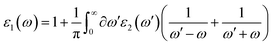 | (4) |
where e, m, V, ψvk, and ψck are electron charge, electron mass, crystal volume, and the wave functions of valence and conduction band states at k, respectively. Also, p⃗ represents momentum operator for energies  and
and  and ℏω signifies the incident photon energy.
For light emission properties, we computed refractive index n(ω), absorption coefficient α(ω) and reflectivity function R(ω) using the relationships.40 The real part of the dielectric function ε1(ω) shown in Fig. 5(a) demonstrates the dispersion of photons as a function of their energies. The static dielectric constant, ε1(0) of the unstrained hexagonal germanium is found to be 13.69, which agrees well with the theoretical values 14.28 and 14.77.41,42 Strain causes structural distortion in the crystal, which changes the relative displacement of the positive and negative centers in an atom. A larger separation between the opposite charges increases electric polarization, and vice versa. Consequently, ε1(0) enhances due to increased tensile whereas compressive strain reduces it (inset diagram of Fig. 5(a)).
 |
| | Fig. 5 (a) Real part of the dielectric function ε1(ω) for hex-Ge under strains. (b) Imaginary part of the dielectric function ε2(ω) for hex-Ge under strains. (c) Refractive index n(ω) for hex-Ge under strains. (d) Strain-dependent absorption coefficient α(ω) for hex-Ge. | |
The imaginary part of the part ε2(ω) of the dielectric function as depicted in Fig. 5(b) deals with the absorption of incident photons by the strained and the unstrained germanium. Red shifting of the absorption edges can be observed both for the tensile and compressive strains (inset picture of Fig. 5(b)), however, the former is more favorable for absorption. Interestingly under tensile strain, the emergence of several shoulder peaks is noticeable which indicates increasing probabilities of absorption. Moreover, this peculiar feature exists not only in the infrared region but also extends till the end of the visible region around 3.1 eV. This might correspond to the increasing number of states in the vicinity of the conduction band minimum under tensile strain. Ultimately, the inversion of the two conduction states, Γ−7c and Γ−8c states have triggered such an observation providing more probabilities for interband transitions.
The refractive index n(ω) is a critical quantity for optical emission, which is used to determine the velocities of photons at different energies. As shown in Fig. 5(c), the obtained static refractive index for the hex-Ge is 3.70, and its value varies proportionally as ε1(ω). In the infrared regime, all strained and unstrained germanium have refractive values in the range of 3.5–4 eV. The application of tensile strain results in the addition of various peaks into the curve in the low energy region, while compression is observed to introduce a single peak in the UV region. This is a consequence of the displacement of the charge centres induced by the strain mechanism as discussed earlier.
The population of electrons in the conduction band is mostly determined by the amount of absorption. The absorption coefficient thus estimates the amount of absorption of photon energies. Fig. 5(d) provides the strain-dependent absorption coefficient α(ω) from the first principles calculations. Infrared photons with energies 0.2–0.8 eV are increasingly absorbed with the tensile strain, in addition to the red shifting caused by band inversion. Strikingly, hex-Ge under tensile strain boosts the absorption by a factor of more than one-fifth with every one percent increase in tensile strain. Peaks at higher energies are flattened by tensile strain.
Of all the photons incident on the material, some photons undergo elastic scattering and are reflected. Reflectivity function R(ω) displays the fraction of the photons that are bounced. The calculated R(ω) depicted in Fig. S2 of ESI† signifies an increasing reflectivity for the hex-Ge with photon energies. It is evident that the tensile strain causes a significant increase in the reflected photons in the infrared regime except in the near-infrared region. The increase in the refractive index forbids the photons from entering the material. On the contrary, reflectivity remained low for the compressed hex-Ge structures.
3.4 Optical gain
The optical gain, the most important parameter for a laser is obtained from the stimulated emission of electrons between the conduction and valence bands. For lasing to take place, Bernard and Duraffourg's criteria of Efc–Efv > Ec–Ev has to be satisfied, where Efc and Efv, are the quasi-Fermi levels for the conduction band and valence bands, respectively, Ec is the conduction band minimum and Ev is the valence band maximum. The optical gain (G) for any bulk semiconductor can be computed using the following equation:43| |
 | (5) |
where, e is the electronic charge, ℏ is the reduced Planck's constant, ε0 is the permittivity of free space, m0 is the rest mass of electron, hν is the photon energy, n0 is the refractive index, mc and mv are the effective masses of electron and hole for the density of states, respectively, and Ec–v is the energy gap between the conduction band and the valence band. |Mc→v|2 is the momentum matrix element between the valence band and the conduction band, which can be computed using the Kane model as follows:44| |
 | (6) |
where, Eg is the band gap between the conduction energy band and the valence band. fh(Ev) and fe(Ec) are the occupation probabilities for the holes and the electrons, which can be calculated by the relations:| |
 | (7) |
Optical gain is primarily obtained from the direct recombination of electrons from the bottom of the conduction band to the top of the valence band. So, we consider the contributions for optical transitions occurring at Γ-point. Considering injected charge carrier density Ninj, charge of neutrality should be followed according to the equations:
| | |
n8c + n7c + n5c = ninj, p9v+ + p7v+ + p7v− = pinj and pinj = ninj
| (8) |
n8c,
n7c, and
n5c are the electron concentrations at conduction band states Γ
−8c, Γ
−8c, and U
−5c, respectively, while
p9v+,
p7v+ and
p7v− are respectively, the hole concentrations at valence band states Γ
+9v, Γ
+7v+, and Γ
+7v−. The electron and hole concentrations are obtained using the relationships:
| |
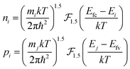 | (9) |
In the above equations, mi and mj are the effective masses of the electron and holes. Following the E–k dispersion relation, the electron energy in the Γ-valley, Ei and hole energy, Ej can be calculated using the following equations:
| |
 | (10) |
| |
 | (11) |
where,
EcΓ is the conduction band minimum at
Γ-point,
Evj is the valence band,
mri and
mrj are the reduced effective masses of electron and hole respectively, calculated from the relationships:
| |
 | (12) |
In the steady state condition, the Fermi–Dirac integral  can be expressed as follows:
| |
 | (13) |
where,
ε = (
E −
EcΓ)/
kT and
ϕ = (
Efc −
EcΓ)/
kT.
Efc and
Efv are solved using
eqn (7) and
(8). The total optical gain of the semiconductor is the sum of the gains resulting from two recombination processes: transition from the conduction band minimum to the light hole and the other from the conduction band minimum to the heavy hole. For all the optical gain calculations, we have considered
Ninj = 5 × 10
18 cm
−3 and a temperature
T = 300 K. The calculated total gain for hex-Ge with and without strains can be observed from
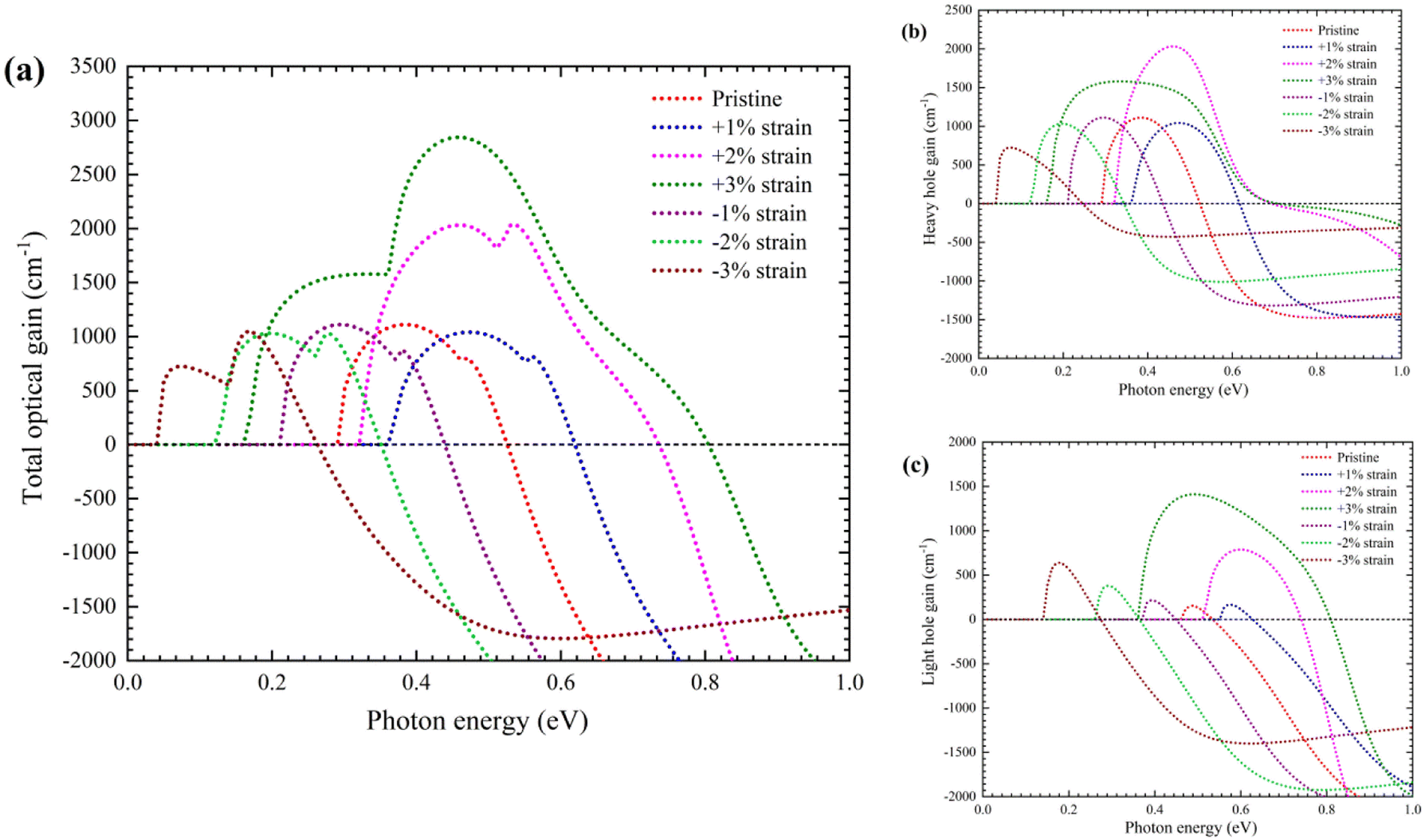
Fig. 6(a). The total gain for the unstrained Ge starts with the optical band gap of 0.29 eV and forms a peak of 1110 cm
−1 at a photon energy of 0.39 eV. This positive gain is possible due to the direct nature of the hex-Ge. Here, we define bandwidth as the energy spectrum for which the positive gain is achieved. With compression, the gain spectrum is red-shifted owing to a decrease in the band gap accompanied by no significant change in amplification and bandwidth. On applying tensile strain, +1% Ge strained structure exhibits a reduction in the peak value. Strikingly, under 2% tensile strain, a two-fold increase in the peak value is attained with respect to pristine hex-Ge along with two times expansion in the gain bandwidth. If we keep increasing tensile strain, then at +3% strain, a gigantic optical gain with a peak of 2845 cm
−1 can be observed spanning a bandwidth of 0.63 eV covering most of the mid-wavelength and short-wavelength infrared regions. These results suggest that strained Ge may be a promising material for mid-wavelength and short-wavelength infrared applications. We plotted the gains contributed by the heavy holes and light holes separately in
Fig. 6(b and c). In
Fig. 6(b), it can be seen that heavy hole gain reduces with compression while tensile strain amplifies gain, although the maximum peak is noticed in the case of +2% strained Ge. The reduction of gain under compression is due to the decrease in the hole carrier concentration of
p9v+ while maintaining a constant level of electron concentration for
n8c (
Fig. 7(a)). Supplementarily, the calculated average squared momentum matrix element, |
MCB→hh|
2 in
Fig. 7(b) also shows a monotonously degrading nature with greater compression for heavy holes. Under tensile strain,
Fig. 7(a) clearly depicts that the electron concentration,
n8c drops significantly caused by the band inversion, simultaneously resulting in the increase of
n7c. Furthermore, tensile strain causes a lowering of the U
−5c state, which allows the accumulation of more electrons under injection. These electrons move towards the Γ-valley and cause an increase in radiative recombination, generating an amplified heavy hole gain. It can be also noticed that |
MCB→hh|
2 increases by applying tensile strain (
Fig. 7(b)). These are the reasons why heavy hole gain increases with applied tensile strain. The nature of the light hole gain can be similarly explained in the light of |
MCB→lh|
2 and change in the electron and hole concentrations. The hole concentration,
p7v+ grows with escalating compression or tensility, which gives rise to increased light hole gain. Astoundingly, the optical gain for light hole intensifies more under tensile strain than compression. This is mainly associated with a high value of |
MCB→lh|
2 signifying a greater strength of optical transition. It can also be noted that |
MCB→lh|
2 is always larger than |
MCB→hh|
2. The amplification for light holes at 2% tensile strain is 5 times that of heavy holes when we compared them to their respective gain under no strain conditions (
Fig. 6(b and c)). This exceptional change in the momentum matrix follows the band inversion of the conduction states that occurs at +1.5% strain. The calculated squared momentum matrix element at +2% strain is 11.2 eV, which approaches that of wurtzite III–V nitrides whose values lie in the range of 14.0–14.6 eV.
35 Thus, the enhanced electron concentration from U
−5c to Γ
−7c state and increased optical interaction between the p-character valence states and the sp-character conduction band states collectively contribute to the amplification of the optical gain under tensile strain.
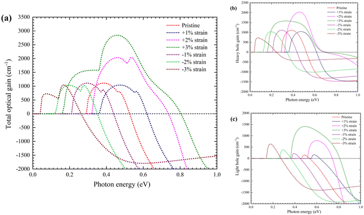 |
| | Fig. 6 (a) Total optical gain for hex-Ge as a function of strain. Strain-dependent (b) heavy hole gain and (c) light hole gain for hex-Ge. | |
 |
| | Fig. 7 (a) Hole and electron concentrations for hex-Ge as a function of strain. (b) Average values of the momentum matrix element for hex-Ge for various strains. Average values of squared momentum matrix element |Mc→v|2 are calculated according to Kane model. Momentum matrix for the conduction band to heavy hole is denoted by |MCB→hh|2 and conduction band to light hole as |MCB→lh|2. | |
4. Conclusions
In summary, the first-principles method DFT was employed to calculate the electronic and optical properties of hex-Ge under uniaxial strain. GGA-PBE-sol functional was used to determine the structural parameters, while mBJ potential with spin–orbit coupling was adopted to successfully predict the band structures in agreement with the experiment values. We observed that tensile strain causes an initial increase in the band gap, while monotonously decreasing after the band inversion of Γ−7c and Γ−8c states around +1.5% strain. Compression reduces the energy level of Γ−8c and increasing Γ−7c energy state, leading to a gradual decrease in the band gap. Concurrently, partial density states and projected density of states show the main character of Ge-4p orbitals in the valence bands, while partly Ge-4p character in addition to the majority s-character is found in the conduction bands. The conduction states show substantial Ge-4p character along the direction Γ to M, which might explain the favoured optical transitions occurring perpendicular to the c-axis. The order of the valence bands under strain remains unaffected and lies in the order: Γ+9v > Γ+7v+ > Γ+7v−. In particular, the crystal field splitting and spin–orbit splitting energies for hex-Ge were noticed to have an opposite trend under strain. The transport nature was revealed by estimating the effective masses along several high symmetry points. The effective mass of electrons for the Γ−7c the state exhibits a tensile-strain-dependent decrease, while the effective mass of holes in the Γ+7v− changes in the opposite direction to that of the (Γ+9v) state. Further, the optical properties for the unstrained and strained were calculated to mainly predict the dielectric nature, absorption, and reflectivity of the semiconductor with respect to strain. The value of ε1(0) is positively affected by tensile strain and conversely, it is decreased by compressive strain. Absorption is enhanced through tensile strain for a broader range of the spectrum. The parameters accurately derived from DFT were employed to calculate the optical gain of hex-Ge under uniaxial compressive and tensile strains. We noticed huge amplification of gain after the band inversion, which arises due to an increase in electron concentration due to U−5c and relatively, a higher contribution from the momentum matrix element. The simplified estimation of the optical gain revealed that the recombination from the conduction band to the light hole band plays a crucial role in this phenomenon. Overall, the insights provided by this study can inform the development of strain-engineered hex-Ge-based electronic and optoelectronic devices with improved performance and efficiency.
Author contributions
Rishikanta Mayengbam: conceptualization, data curation, formal analysis, investigation, methodology, validation, visualization, and writing-original draft, review, and editing. Chuan Seng Tan: funding acquisition, data curation, formal analysis, and investigation. Weijun Fan: conceptualization, funding acquisition, methodology, project administration, resources, software, supervision, and writing – review and editing.
Conflicts of interest
The authors declare there are no conflicts of interest.
Acknowledgements
WJ Fan would like to acknowledge the support from NRF-CRP19-2017-01.
References
- D. Buca, R. Soref and S.-Q. Yu, Group IV photonics: driving integrated optoelectronics, Opt. Photonics News, 2016, 27, 32–39 Search PubMed.
- D. A. B. Miller, Device requirements for optical interconnects to silicon chips, Proc. IEEE, 2009, 97, 1166–1185 CAS.
- A. H. Atabaki, S. Moazeni, F. Pavanello, H. Gevorgyan, J. Notaros, L. Alloatti, M. T. Wade, C. Sun, S. A. Kruger, H. Meng, K. al Qubaisi, I. Wang, B. Zhang, A. Khilo, C. V. Baiocco, M. A. Popović, V. M. Stojanović and R. J. Ram, Integrating photonics with silicon nanoelectronics for the next generation of systems on a chip, Nature, 2018, 556, 349–354 CrossRef CAS PubMed.
- L. Pavesi, L. Dal Negro, C. Mazzoleni, G. Franzò and F. Priolo, Optical gain in silicon nanocrystals, Nature, 2000, 408, 440–444 CrossRef CAS PubMed.
- H. I. T. Hauge, M. A. Verheijen, S. Conesa-Boj, T. Etzelstorfer, M. Watzinger, D. Kriegner, I. Zardo, C. Fasolato, F. Capitani, P. Postorino, S. Kölling, A. Li, S. Assali, J. Stangl and E. P. A. M. Bakkers, Hexagonal silicon realized, Nano Lett., 2015, 15, 5855–5860 CrossRef CAS PubMed.
- X. Xu, S. Narusawa, T. Chiba, T. Tsuboi, J. Xia, N. Usami, T. Maruizumi and Y. Shiraki, Silicon-based light-emitting devices based on ge self-assembled quantum dots embedded in optical cavities, IEEE J. Quantum Electron., 2012, 18, 1830–1838 CAS.
- M. R. Bauer, J. Tolle, C. Bungay, A. V. G. Chizmeshya, D. J. Smith, J. Menéndez and J. Kouvetakis, Tunable band structure in diamond–cubic tin–germanium alloys grown on silicon substrates, Solid State Commun., 2003, 127, 355–359 CrossRef CAS.
- C. Rödl, J. Furthmüller, J. R. Suckert, V. Armuzza, F. Bechstedt and S. Botti, Accurate electronic and optical properties of hexagonal germanium for optoelectronic applications, Phys. Rev. Mater., 2019, 3, 034602 CrossRef.
- B. Haberl, M. Guthrie, B. D. Malone, J. S. Smith, S. V. Sinogeikin, M. L. Cohen, J. S. Williams, G. Shen and J. E. Bradby, Controlled formation of metastable germanium polymorphs, Phys. Rev. B: Condens. Matter Mater. Phys., 2014, 89, 144111 CrossRef.
- L. Vincent, G. Patriarche, G. Hallais, C. Renard, C. Gardès, D. Troadec and D. Bouchier, Novel heterostructured Ge nanowires based on polytype transformation, Nano Lett., 2014, 14, 4828–4836 CrossRef CAS PubMed.
- E. M. T. Fadaly, A. Dijkstra, J. R. Suckert, D. Ziss, M. A. J. van Tilburg, C. Mao, Y. Ren, V. T. van Lange, K. Korzun, S. Kölling, M. A. Verheijen, D. Busse, C. Rödl, J. Furthmüller, F. Bechstedt, J. Stangl, J. J. Finley, S. Botti, J. E. M. Haverkort and E. P. A. M. Bakkers, Direct-bandgap emission from hexagonal Ge and SiGe alloys, Nature, 2020, 580, 205–209 CrossRef CAS PubMed.
- H. I. T. Hauge, S. Conesa-Boj, M. A. Verheijen, S. Koelling and E. P. A. M. Bakkers, Single-crystalline hexagonal silicon-germanium, Nano Lett., 2017, 17, 85–90 CrossRef CAS PubMed.
- R. Geiger, T. Zabel and H. Sigg, Group IV direct band gap photonics: methods, challenges, and opportunities, Front. Mater., 2015, 2, 52 Search PubMed.
- J. R. Suckert, C. Rödl, J. Furthmüller, F. Bechstedt and S. Botti, Efficient strain-induced light emission in lonsdaleite germanium, Phys. Rev. Mater., 2021, 5, 024602 CrossRef CAS.
- G. Signorello, E. Lörtscher, P. A. Khomyakov, S. Karg, D. L. Dheeraj, B. Gotsmann, H. Weman and H. Riel, Inducing a direct-to-pseudodirect bandgap transition in wurtzite GaAs nanowires with uniaxial stress, Nat. Commun., 2014, 5, 1–8 Search PubMed.
- Q. M. Thai, J. Chretien, M. Bertrand, L. Casiez, A. Chelnokov, V. Reboud, N. Pauc and V. Calvo, GeSn optical gain and lasing characteristics modelling, Phys. Rev. B, 2020, 102, 155203 CrossRef CAS.
- P. Borlido, J. R. Suckert, J. Furthmüller, F. Bechstedt, S. Botti and C. Rödl, From pseudo-direct hexagonal germanium to direct silicon-germanium alloys, Phys. Rev. Mater., 2021, 5, 114604 CrossRef CAS.
- T. Imajo, T. Suemasu and K. Toko, Strain effects on polycrystalline germanium thin films, Sci. Rep., 2021, 11, 1–6 CrossRef PubMed.
- F. T. Armand Pilon, Y. M. Niquet, J. Chretien, N. Pauc, V. Reboud, V. Calvo, J. Widiez, J. M. Hartmann, A. Chelnokov, J. Faist and H. Sigg, Investigation of lasing in highly strained germanium at the crossover to direct band gap, Phys. Rev. Res., 2022, 4, 033050 CrossRef CAS.
- S. Mellaerts, V. Afanas'ev, J. W. Seo, M. Houssa and J. P. Locquet, Efficient direct band-gap transition in germanium by three-dimensional strain, ACS Appl. Mater. Interfaces, 2021, 13, 30941–30949 CrossRef CAS PubMed.
- T. Inaoka, T. Furukawa, R. Toma and S. Yanagisawa, Tensile-strain effect of inducing the indirect-to-direct band-gap transition and reducing the band-gap energy of Ge, J. Appl. Phys., 2015, 118, 105704 CrossRef.
- L. Liu, M. Zhang, L. Hu, Z. Di and S. J. Zhao, Effect of tensile strain on the electronic structure of Ge: a first-principles calculation, J. Appl. Phys., 2014, 116, 113105 CrossRef.
- H. Tahini, A. Chroneos, R. W. Grimes, U. Schwingenschlögl and A. Dimoulas, Strain-induced changes to the electronic structure of germanium, J. Phys.: Condens. Matter, 2012, 24, 195802 CrossRef CAS PubMed.
- W. Huang, B. Cheng, C. Xue and Z. Liu, Comparative studies of band structures for biaxial (100)-, (110)-, and (111)-strained GeSn: a first-principles calculation with GGA + U approach, J. Appl. Phys., 2015, 118, 165704 CrossRef.
- P. Logan and X. Peng, Strain-modulated electronic properties of Ge nanowires: a first-principles study, Phys. Rev. B: Condens. Matter Mater. Phys., 2009, 80, 115322 CrossRef.
- A. Belabbes, F. Bechstedt and S. Botti, Giant optical oscillator strengths in perturbed hexagonal germanium, Phys. Status Solidi RRL, 2022, 16, 2100555 CrossRef CAS.
- G. Kresse and J. Furthmüller, Efficiency of ab initio total energy calculations for metals and semiconductors using a plane-wave basis set, Comput. Mater. Sci., 1996, 6, 15–50 CrossRef CAS.
- J. P. Perdew, A. Ruzsinszky, G. I. Csonka, O. A. Vydrov, G. E. Scuseria, L. A. Constantin, X. Zhou and K. Burke, Restoring the density-gradient expansion for exchange in solids and surfaces, Phys. Rev. Lett., 2008, 100, 136406 CrossRef PubMed.
- F. Tran and P. Blaha, Accurate band gaps of semiconductors and insulators with a semilocal exchange-correlation potential, Phys. Rev. Lett., 2009, 102, 226401 CrossRef PubMed.
- P. Borlido, T. Aull, A. W. Huran, F. Tran, M. A. Marques and S. Botti, Large-scale benchmark of exchange–correlation functionals for the determination of electronic band gaps of solids, J. Chem. Theory Comput., 2019, 15, 5069–5079 CrossRef CAS PubMed.
- S. Q. Wang and H. Q. Ye, Ab initio elastic constants for the lonsdaleite phases of C, Si and Ge, J. Phys.: Condens. Matter, 2003, 15, 5307 CrossRef CAS.
- S. L. Chuang and C. S. Chang, K p method for strained wurtzite semiconductors, Phys. Rev. B: Condens. Matter Mater. Phys., 1996, 54, 2491 CrossRef CAS PubMed.
- P. Tronc, Y. E. Kitaev, G. Wang, M. F. Limonov, A. G. Panfilov and G. Neu, Optical selection rules for hexagonal GaN, Phys. Status Solidi B, 1999, 216, 599–603 CrossRef CAS.
- W. J. Yin, T. Shi and Y. Yan, Unique properties of halide perovskites as possible origins of the superior solar cell performance, Adv. Mater., 2014, 26, 4653–4658 CrossRef CAS PubMed.
- I. Vurgaftman, J. R. Meyer and L. R. Ram-Mohan, Band parameters for III–V compound semiconductors and their alloys, J. Appl. Phys., 2001, 89, 5815 CrossRef CAS.
- Q. Yan, P. Rinke, M. Winkelnkemper, A. Qteish, D. Bimberg, M. Scheffler and C. G. van de Walle, Strain effects and band parameters in MgO, ZnO, and CdO, Appl. Phys. Lett., 2012, 101, 152105 CrossRef.
- L. Cláudio De Carvalho, A. Schleife, F. Fuchs and F. Bechstedt, Valence-band splittings in cubic and hexagonal AlN, GaN, and InN, Appl. Phys. Lett., 2010, 97, 232101 CrossRef.
- Y. F. Lao and A. G. Unil Perera, Dielectric function model for p-type semiconductor inter-valence band transitions, J. Appl. Phys., 2011, 109, 103528 CrossRef.
- M. Gajdoš, K. Hummer, G. Kresse, J. Furthmüller and F. Bechstedt, Linear optical properties in the projector-augmented wave methodology, Phys. Rev. B: Condens. Matter Mater. Phys., 2006, 73, 045112 CrossRef.
- R. E. Hummel, Electronic Properties of Materials, Springer, 2011 Search PubMed.
- A. De and C. E. Pryor, Electronic structure and optical properties of Si, Ge and diamond in the lonsdaleite phase, J. Phys.: Condens. Matter, 2014, 26, 045801 CrossRef CAS PubMed.
- N. Bao, F. Guo, D. Kang, Y. Feng, H. Wang and J. Dai, Toward accurate electronic, optical, and vibrational properties of hexagonal Si, Ge, and Si1−xGex alloys from first-principle simulations, J. Appl. Phys., 2021, 129, 145701 CrossRef CAS.
- W. Huang, H. Yang, B. Cheng and C. Xue, Theoretical study of the effect of different n-doping elements on band structure and optical gain of GeSn alloys, Phys. Chem. Chem. Phys., 2017, 19, 27031–27037 RSC.
- S. L. Chuang, Physics of photonic devices, John Wiley & Sons, 2012 Search PubMed.
|
| This journal is © The Royal Society of Chemistry 2023 |
Click here to see how this site uses Cookies. View our privacy policy here. 
 Open Access Article
 This Open Access Article is licensed under a Creative Commons Attribution-Non Commercial 3.0 Unported Licence
 ,
Chuan Seng Tan and
Weijun Fan
,
Chuan Seng Tan and
Weijun Fan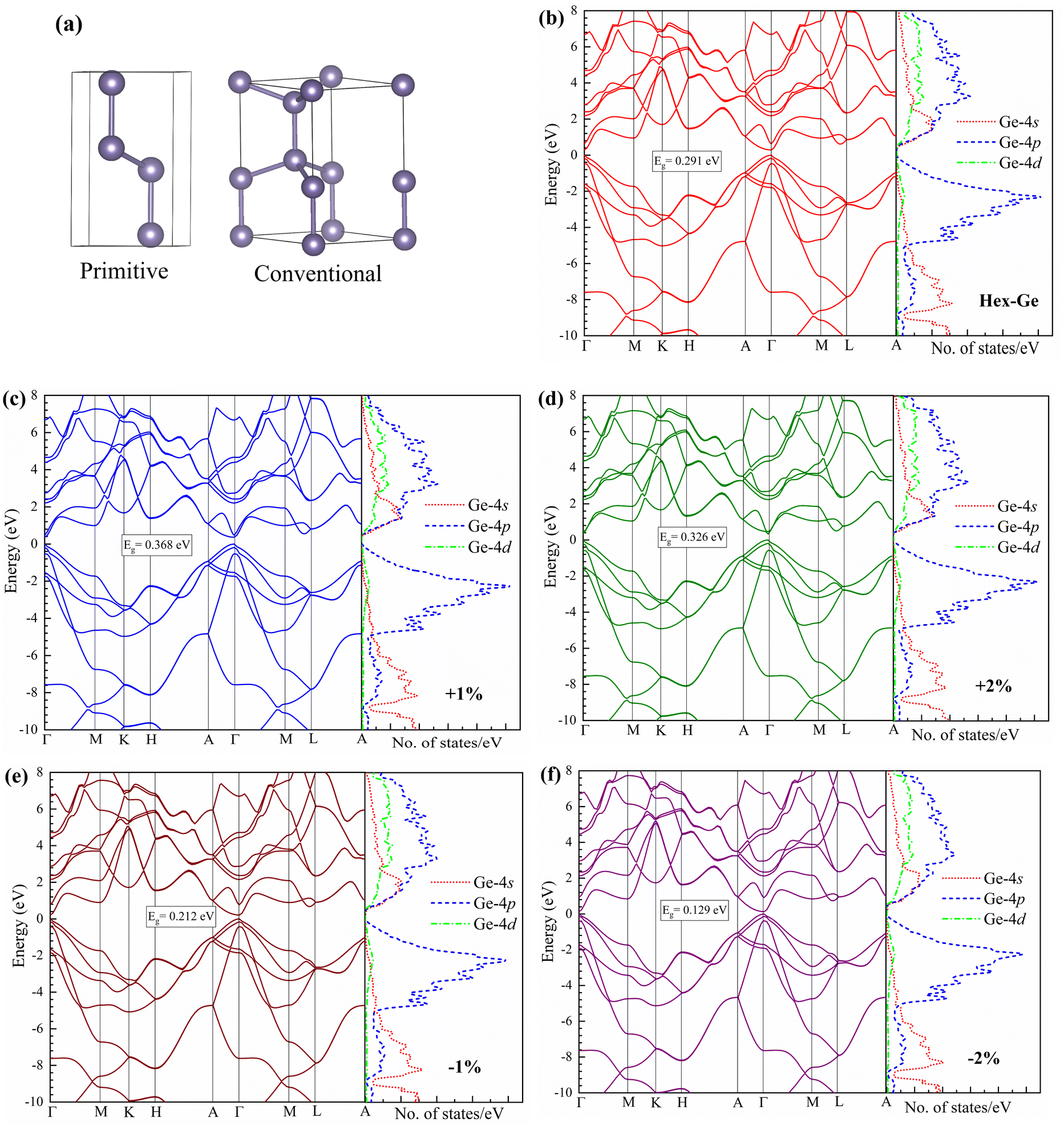


 The introduction of uniaxial strain along the c-axis induces fluctuations in the value of Δ∥SO. Nevertheless, the direction-average spin–orbit splitting energy ΔSO lies in the narrow energy range of 0.32–0.35 eV. Last, but not least, the combined effect of ΔSO and ΔCF are clearly responsible for engineering the energy levels of the three valence states. Significantly, the energy difference between them can cause intervalence band (IVB) transitions, which is detrimental to optical gain.38 Effective charge transport is a critical material property that plays a key role in the operation of laser devices. For all the relaxed structures, both strained and unstrained, effective masses are calculated by the parabolic fit of the energy-dispersion relation given by the equation.

 along all symmetry points as shown in Fig. 4(a–c). However, the effect of strain is not significant in the case of
 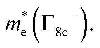 The reduction in the effective mass of electrons in the Γ−7c state under tensile strain could improve carrier mobility. In valence states, the effect of strain is more pronounced in split-off hole state, Γ+7v−. It increases monotonously along the M and X directions, going from compressive to tensile strain, while the reverse trend can also be observed along the A point. Surprisingly, an exact opposite trend to Γ+7v− is noticed in the
  In the valence band, we can observe that the trend of effective masses along A is directly opposite to that of the M and X directions. This peculiar behavior has occurred because of the application of strain along the c-axis which is parallel to A.

 and
and  and ℏω signifies the incident photon energy.


 can be expressed as follows: