
 Open Access Article
 This Open Access Article is licensed under a Creative Commons Attribution-Non Commercial 3.0 Unported Licence
Synaptic plasticity realized by selective oxidation of TiS3 nanosheet for neuromorphic devices†
Jing-Kai Qina,
Hai-Lin Suna,
Pei-Yu Huanga,
Yang Li b,
Liang Zhenab and
Cheng-Yan Xu*ab
b,
Liang Zhenab and
Cheng-Yan Xu*ab
aSauvage Laboratory for Smart Materials, School of Materials Science and Engineering, Harbin Institute of Technology (Shenzhen), Shenzhen 518055, China. E-mail: cy_xu@hit.edu.cn
bMOE Key Laboratory of Micro-System and Micro-Structures Manufacturing, Harbin Institute of Technology, Harbin 150080, China
First published on 15th May 2023
Abstract
Memristive devices operating analogous to biology synapses demonstrate great potential for neuromorphic applications. Here, we reported the space-confined vapor synthesis of ultrathin titanium trisulfide (TiS3) nanosheets, and subsequent laser manufacturing of a TiS3–TiOx–TiS3 in-plane heterojunction for memristor applications. Due to the flux-controlled migration and aggregation of oxygen vacancies, the two-terminal memristor demonstrates reliable “analog” switching behaviors, in which the channel conductance can be incrementally adjusted by tuning the duration and sequence of programming voltage. The device allows the emulation of basic synaptic functions, featuring excellent linearity and symmetry in conductance change during long-term potentiation/depression processes. The small asymmetric ratio of 0.15 enables it to be integrated into a neural network for the pattern recognition task with a high accuracy of 90%. The results demonstrate the great potential of TiS3-based synaptic devices for neuromorphic applications.
Introduction
Neuromorphic computing inspired by the human brain is expected to overcome the bottleneck of storage and power consumption in conventional von Neumann computing systems.1–5 As the most important cornerstone of neuromorphic computing hardware architecture, the memristor operates analogous to biology synapses, in which the conductance can be incrementally modified by controlling the charge or flux through it.6–9 A wealth of materials have been developed for the device implementation of memristors. Among them, two-dimensional (2D) layered semiconductors stand out because of their outstanding electrical and optoelectrical properties. Titanium trisulfide (TiS3) has been reported as a 2D semiconductor with strong in-plane anisotropy. It reveals a direct electric band gap of 1.0 eV, and an extremely high electron mobility more than 10![[thin space (1/6-em)]](https://www.rsc.org/images/entities/char_2009.gif) 000 cm2 V−1 s−1 has been predicted by ab initio calculations.10–12 However, the difference in the Ti–S bond length results in highly-aligned 1D chains with strong in-plane anisotropy,13 thus the traditional synthesis methods typically yield quasi-1D nanowires or nanoribbons, which causes a great challenge for integration with other 2D materials.
000 cm2 V−1 s−1 has been predicted by ab initio calculations.10–12 However, the difference in the Ti–S bond length results in highly-aligned 1D chains with strong in-plane anisotropy,13 thus the traditional synthesis methods typically yield quasi-1D nanowires or nanoribbons, which causes a great challenge for integration with other 2D materials.
Note that titanium oxide (TiOx) has been well studied as candidate of memristor to construct artificial synapses.14–16 The migration and diffusion process of oxygen ions enable the modulation of electrical conductance, thus allowing the mimicking of synaptic functions of biology neurons, such as short-term plasticity (STP), long-term plasticity (LTP), pulse-paired facilitation (PPF),17,18 etc. Previous studies have revealed the feasibility of controllably oxidization technique to create 2D oxide and related heterostructures,19,20 thus it is expected that TiOx and related heterostructures can also be achieved in 2D configuration based on 2D TiS3 nanosheets. The 2D TiS3–TiOx heterostructure can be easily integrated with silicon platform and other 2D materials, and be applied for constructing synaptic device multiple functions.
In this work, we reported the space-confined synthesis of ultrathin TiS3 nanosheets with high crystalline quality. Top-gated field effect transistor (FETs) based on TiS3 nanosheet delivers a large on-state current density of 510 mA mm−1 and high carrier mobility close to 100 cm2 V−1 s−1. By using a laser-assisted manufacture technique, in-plane TiS3–TiOx–TiS3 heterojunction can be created for memristor construction, which demonstrates excellent synaptic characteristics with tunable and multiple resistance levels. The device can also be integrated into neural network for high-accuracy pattern recognition. The results indicate that TiS3-based memristors might be ideal building blocks for a neuromorphic computing system.
Results and discussion
Atomically thin TiS3 nanosheets were obtained through a space-confined chemical vapor transport (SC-CVT) method,13 where the confined space can be created by stacking two freshly-exfoliated mica substate vertically (Fig. 1a). Stoichiometric Ti powders and S powders were sealed at the end of a quartz tube with pressure less than 10 mbar, and amount of I2 was also added as transport agent. The quartz tube was then heated at 550 °C for 1 h. After cooling, TiS3 nanosheets with thicknesses ranging from 8 to 30 nm can grow on the surface of sandwiched mica sheets. The as-synthesized samples on mica substrate present a small thickness in the range from 6 to 30 nm. Fig. 1b show an optical microscopy (OM) and corresponding atomic force microscopy (AFM) images of a 14 nm-thick TiS3 nanosheet, which demonstrate an atomically-flat surface. The Raman spectrum was also collected from the sample (Fig. 1c). Four active Raman modes were clearly detected, located at 176, 298, 370, and 556 cm−1, respectively. This is in well consistence with previously reported TiS3 crystal and nanowires,21–23 further confirming the phase of TiS3 nanosheets.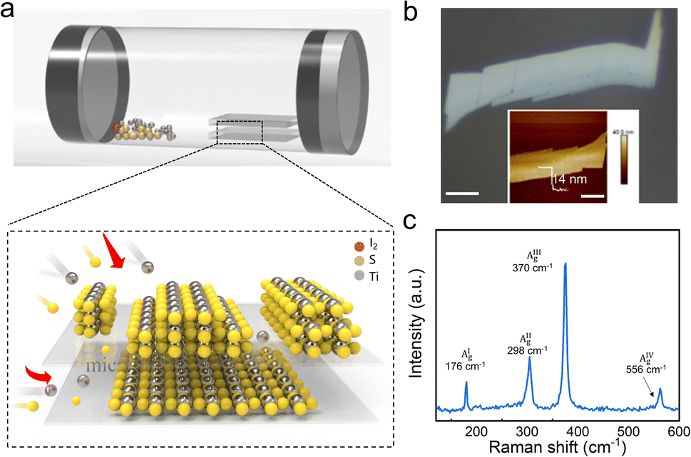 | ||
| Fig. 1 Synthesis and materials characterization of TiS3 nanosheets. (a) Schematic of SCCVT to synthesize TiS3 nanosheets in confined space of mica substates using I2 as carrier. (b) OM image of TiS3 nanosheet. The inset image shows the corresponding AFM image. Scale bars: 10 μm (c) Raman spectrum collected from TiS3 nanosheet. | ||
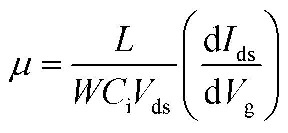
We first investigated the electrical transport properties of TiS3 nanosheet by constructing a top-gated field effect transistor (FETs). To provide effective gate controlling of channel conductance, a 10 nm-thick h-BN flake serving as gate dielectric was exfoliated on the top of TiS3 nanosheet with thickness of 8 nm for device fabrication (Fig. 2a). Au/Ti (50/10 nm) electrodes are patterned and deposited through the standard laser direct writing lithography and metal deposition processes, and the channel length is set to be 5 μm. All the electrical measurements are conducted in a Lakeshore probe station connected to a Keithley 4200A parameter analyser under dark and high vacuum conditions. Fig. 2b shows the OM image of a just-fabricated device. The linear Ids–Vds characteristics indicates that near ohmic contacts are formed at heterojunction between TiS3 nanosheet and Ti/Au electrodes (Fig. 2c). The transfer curves of the same device are shown in Fig. 2d. We can see that the device presents typical n-type transport behavior with a high current on–off ratio about 105, together with a large on-state current density up to 510 mA mm−1. The two-terminal field-effect mobility can be calculated by the following equation:24
 | (1) |
 | ||
| Fig. 2 Electrical performance of top-gated TiS3 FETs. (a) Schematic of top-gated FETs, where 10 nm-thick h-BN nanosheet is capped on top of TiS3 channel as dielectric. (b) OM image of the device. (c) Current–voltage (Ids–Vds) characteristics of device. (d) Transfer (Ids–Vtg) characteristics for the same device. | ||
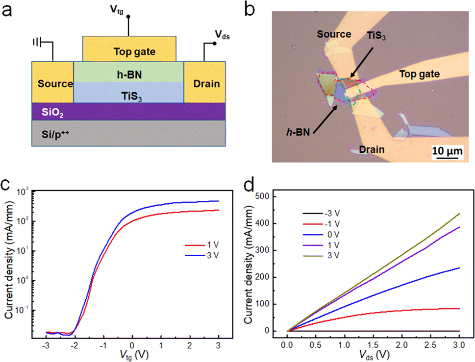
We then constructed a planar TiS3–TiOx–TiS3 heterostructure based on the selective oxidization of TiS3 nanosheet. Selective oxidation of TiS3 nanosheet was implemented with the assistance of the 532 nm laser equipped on a micro-Raman spectrometer. The laser beam has a spot size of 500 nm, focusing on the surface and scan cross the sample with a grating of 1500 lines per mm. Surface oxidation can be realized under ambient environment due to the local high temperature arised from laser irradiation.25,26 By setting the scanning rate and size, the surface of TiS3 nanosheet can be selectively oxidized into TiOx to form the in-plane heterostructures (Fig. 3a). Fig. 3b shows the OM image of a TiS3 nanosheet, in which the surface is selectively oxidated to form a pattern of “HIT”. The pattern can be clearly resolved due to the different light interference from TiS3 and TiOx. From the AFM image shown in Fig. 3c, we can see that laser irradiation causes remarkable change of morphology in TiS3 nanosheet, and the surface roughness increase significantly from 0.3 to 2.2 nm. It should be noted the pristine TiS3 without laser irradiation is barely affected given the small spot size of laser beam, thus creating a clear border line at the heterojunction area. The Raman spectrum of sample after laser oxidation was collected for comparison21,27 (Fig. 3d), from which we can clearly resolved an active Raman mode belonging to TiO2 at 143 cm−1. The corresponding intensity mapping images of modes are shown in Fig. 3f. The 370 cm−1 mode of TiS3 is barely identified, while the intensity of 143 cm−1 peaks increase significantly. The results strongly confirm the transformation from TiS3 to TiOx by laser irradiation and the formation of in-plane TiS3–TiOx–TiS3 heterostructure.
 | ||
| Fig. 3 Selective oxidation of TiS3 nanosheet for constructing in-plane heterojunction. (a) Scheme of laser oxidation from TiS3 to TiOx. (b) OM image of a TiS3 nanosheet after laser oxidation. (c and d) AFM topography and corresponding height profile of in-plane TiS3–TiOx heterojunction. (e) Raman spectrum collected from the oxidized area. (f) The intensity mapping of Raman peaks at 370 and 143 cm−1. | ||
The selective oxidation from TiS3 to TiOx can be explained by thermal effect induced by laser irradiation.26 That is, laser energy absorbed by TiS3 would cause the local temperature rise and intense lattice vibration, and TiS3 would react with oxygen in ambient environment and be oxidized into TiOx. The local temperature rise is highly related to laser fluence (F), and it can be estimated by28
 | (2) |
Two-terminal TiS3 device was first fabricated in planar configuration. The channel of device is patterned to 5 μm, and the center of channel is selectively oxidated by laser irradiation with width of 1 μm. The resulting TiS3–TiOx–TiS3 heterostructure demonstrates remarkable resistive switching behavior. As shown in Fig. 4a, the channel current continuously increases by six times as applied with 6 consecutives positive voltage sweeps (0–3 V), suggesting the resistance can be effectively modulated through voltage stressing. By applying six consecutive negative voltage sweeps (0 to −3 V), the resistance would recover back to the initial state (Fig. 4b). The nonlinear modulation of resistance in our memristor is very similar to the transmission characteristics of biological synapses.29,30 As shown in the inset image of Fig. 4b, the paired electrodes can be treated as the pre- and postsynaptic neurons, and the positive or negative voltage stimulus are used to excite or inhibit the synapses.
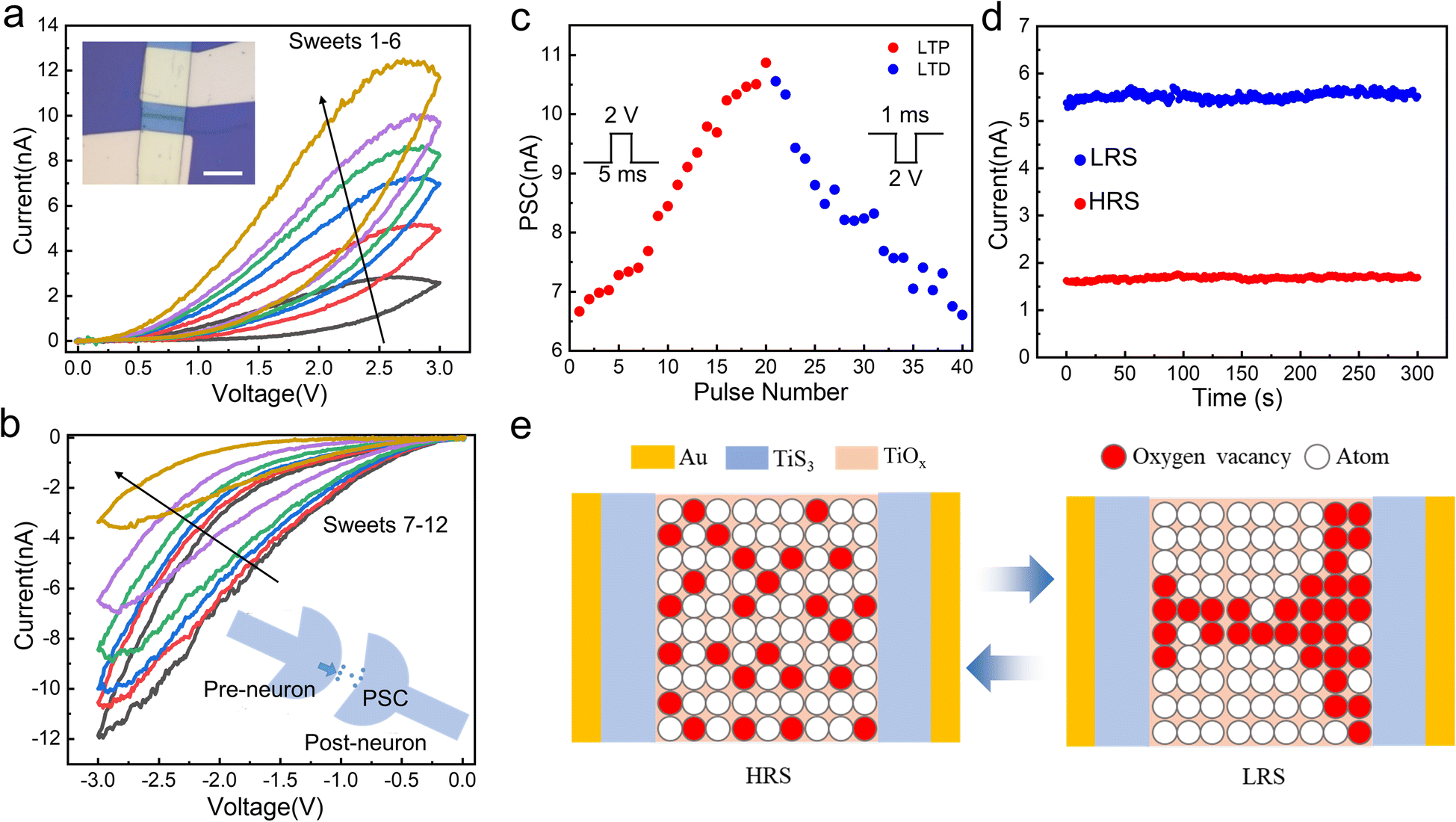 | ||
| Fig. 4 The synaptic characteristics of TiS3–TiOx–TiS3 memristor. (a) I–V characteristics of the memristor at positive bias voltages sweeps. The inset image shows the OM image of a device. (b) I–V characteristics of the same device at consecutive negative voltages sweeps. Inset image illustrates a biology synapse. (c) Modulation of synaptic weight under positive and negative voltage pulses. (d) Retention performance of the device. The high resistance is identified as the initial state without voltage applying, and low resistance is achieved by consecutively applying 20 positive voltage pulses. (e) Resistance switching mechanism of memristor. | ||
Long-term potentiation (LTP) and long-term depression (LTD) characteristic of synapse, which represent the persistent strengthening and weakening of synapses that lead to the long-lasting change of signal transmission between neurons, can also be mimicked by the in-plane memristor. LTP behavior was investigated under 20 identical positive voltage pulse (duration of 5 ms, amplitude of 2 V), and channel current of the device is tracked every 1 s. For the LTD process, negative voltage pulse (duration of 1 ms, amplitude of −2 V) was utilized. To exclude the influence of the voltage stressing, we measured the current change with a small reading voltage of 0.1 V. As shown in Fig. 4c, the conductance and synaptic weight increase gradually under voltage stimulation, with a remarkable change of postsynaptic current (PSC) from 6 to 11 nA. Fig. 4d shows the endurance performance of memristor. We can see that the resistance values for both high resistive state (HRS) and low resistive state (LRS) can be well retained without degradation after 300 s, indicating good electrical stability of the device. The linear and symmetric conductance update during LTP and LTD are crucial to achieve high learning accuracy for neuromorphic computing.31,32 The asymmetric ratio (A) is defined by the following equation:33
 | (3) |
The modulation mechanism of electrical conductance in TiS3–TiOx–TiS3 planer heterostructure is highly associated with the directional migration and diffusion of oxygen vacancies.34,35 In the initial HRS, the inherent oxygen vacancies, which introduced during the laser oxidation process, are locally distributed in the TiOx region. These oxygen vacancies can be easily driven under electric field at room temperature, and migrate along channel direction.17 Meanwhile, the aggregation of oxygen vacancies would contribute to the pathways with high electrical conductivity. The oxygen vacancies acting as n-type dopants would introduce shallow donor states close to the conduction band of TiOx, thus leading to the reduction of barrier height at TiOx–TiS3 heterojunction and LRS of device35,36 (ESI Fig. S3†). Therefore, we can expect the effective non-volatile modulation of resistance in our TiS3–TiOx–TiS3 memristor.
The excellent linearity and symmetry in conductance change during long-term potentiation/depression processes enables the device to be integrated into neural network for the high-accuracy pattern recognition. The handwritten letters are resized into 20 × 20 pixels by cropping the edges of the original image in Extended Modified National Institute of Standards and Technology (EMNIST) dataset (Fig. 5a). The network consists of 400 input neurons corresponding to 20 × 20 pixels of resized EMNIST image and 10 output neurons with connections through 100 hidden neurons (ESI Fig. S4†). During the simulation, each neuron of input layers represents an individual device to receive the electrical stimuli corresponding to the grey value of pixel, and transmits the electrical signals to the next layer neurons regarding the conductance status. The updated synaptic weights in network enable output neurons to generate the evolved image. As shown in Fig. 5b, the output digits can be barely distinguishable as trained by 5 epochs. After applied by 10 epochs, synaptic weights were remarkably strengthened, contributing to a much clearer digits with high contrast. The neural network based on our memristor demonstrates a high recognition accuracy of ∼90% with the increasing learning epoch (Fig. 5c). The recognition accuracy is outstanding in previously reported two-terminal resistive switching memoriter and the phase change memory devices.37–39 The successful emulation of synaptic functions together with high accuracy of image recognition strongly confirm that our TiS3–TiOx–TiS3 in-plane memristor can be utilized for neuromorphic computing applications.
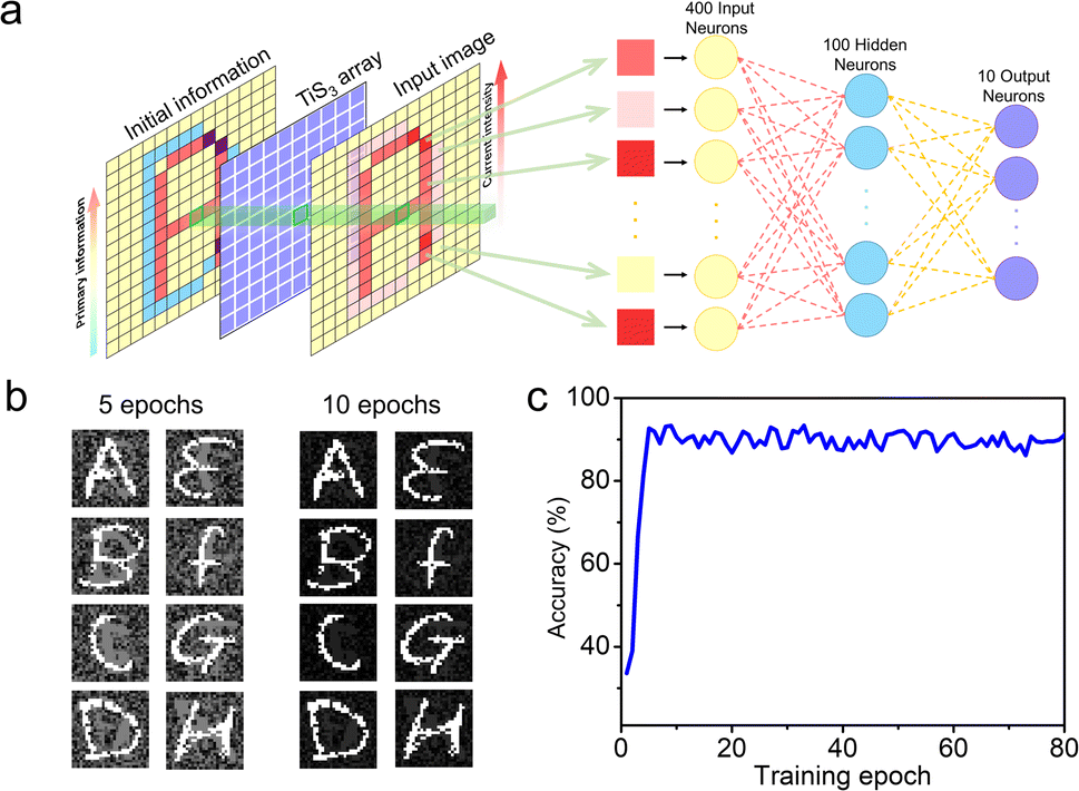 | ||
| Fig. 5 Neuromorphic computing simulation based on the TiOx–TiS3–TiOx memristor. (a) Schematic diagram of constructed convolutional neural network. (b) Mapping images with different synaptic weight updates as trained for 5 and 10 epochs. (c) The recognition accuracy evolution with training epochs based on our device. | ||
Conclusions
In summary, TiS3 nanosheets with high crystalline quality were synthesized using space-confined vapor transport approach. Based on the samples, we fabricated in-plane TiS3–TiOx–TiS3 heterostructure with the assistance of a laser-assisted manufacture technique. Attributing to directional migration and aggregation of oxygen vacancies, the device demonstrates excellent synaptic characteristics with tunable channel resistance. The excellent multiple resistance levels also allows it to be integrated into neural network for the pattern recognition task, which shows a high recognition accuracy of 90%. Our work provides a simple and effective approach to develop 2D material-based memory and synaptic devices for neuromorphic applications.Conflicts of interest
There are no conflicts to declare.Acknowledgements
This work was supported by National Natural Science Foundation of China (No. 52102161), Shenzhen Training Programme Foundation for the Innovative Talents (No. RCBS20200714114911270), Natural Science Foundation of Guangdong Province (No. 2021A1515012423), and Stabilization Support Programme of Higher Education Institutes in Shenzhen (No. GXWD20201230155427003-20200805161204001).References
- F. Chen, Y. Zhou, Y. Zhu, R. Zhu, P. Guan, J. Fan, L. Zhou, N. Valanoor, F. Von Wegner and E. Saribatir, J. Mater. Chem. C, 2021, 9, 8372–8394 RSC.
- Z. Wang, S. Joshi, S. E. Savel’ev, H. Jiang, R. Midya, P. Lin, M. Hu, N. Ge, J. P. Strachan and Z. Li, Nat. Mater., 2017, 16, 101–108 CrossRef CAS PubMed.
- Q. Wan, M. T. Sharbati, J. R. Erickson, Y. Du and F. Xiong, Adv. Mater. Technol., 2019, 4, 1900037 CrossRef.
- J.-K. Qin, F. Zhou, J. Wang, J. Chen, C. Wang, X. Guo, S. Zhao, Y. Pei, L. Zhen and P. D. Ye, ACS Nano, 2020, 14, 10018–10026 CrossRef CAS PubMed.
- M. Si, Y. Luo, W. Chung, H. Bae, D. Zheng, J. Li, J. Qin, G. Qiu, S. Yu and P. Ye, Presented in part at the 2019 IEEE International Electron Devices Meeting, IEDM, 2019 Search PubMed.
- P. Yao, H. Wu, B. Gao, J. Tang, Q. Zhang, W. Zhang, J. J. Yang and H. Qian, Nature, 2020, 577, 641–646 CrossRef CAS PubMed.
- W. Huh, D. Lee and C. H. Lee, Adv. Mater., 2020, 32, 2002092 CrossRef CAS PubMed.
- J. K. Qin, B. X. Zhu, C. Wang, C. Y. Zhu, R. Y. Sun, L. Zhen, Y. Chai and C. Y. Xu, Adv. Electron. Mater., 2022, 8, 2200721 CrossRef CAS.
- J. Lao, W. Xu, C. Jiang, N. Zhong, B. Tian, H. Lin, C. Luo, J. Travas-sejdic, H. Peng and C.-G. Duan, J. Mater. Chem. C, 2021, 9, 5706–5712 RSC.
- J. O. Island, M. Barawi, R. Biele, A. Almazán, J. M. Clamagirand, J. R. Ares, C. Sánchez, H. S. Van Der Zant, J. V. Álvarez and R. D'Agosta, Adv. Mater., 2015, 27, 2595–2601 CrossRef CAS PubMed.
- J. O. Island, R. Biele, M. Barawi, J. M. Clamagirand, J. R. Ares, C. Sánchez, H. S. van der Zant, I. J. Ferrer, R. D'Agosta and A. Castellanos-Gomez, Sci. Rep., 2016, 6, 22214 CrossRef CAS PubMed.
- N. Tripathi, V. Pavelyev, P. Sharma, S. Kumar, A. Rymzhina and P. Mishra, Mater. Sci. Semicond. Process., 2021, 127, 105699 CrossRef CAS.
- J.-K. Qin, H.-L. Sun, T. Su, W. Zhao, L. Zhen, Y. Chai and C.-Y. Xu, Appl. Phys. Lett., 2021, 119, 201903 CrossRef CAS.
- G. Zhou, B. Sun, X. Hu, L. Sun, Z. Zou, B. Xiao, W. Qiu, B. Wu, J. Li and J. Han, Adv. Sci., 2021, 8, 2003765 CrossRef CAS.
- T. Dongale, N. Desai, K. Khot, C. Volos, P. Bhosale and R. Kamat, J. Nanoelectron. Optoelectron., 2018, 13, 68–75 CrossRef CAS.
- M. K. Akbari, R. K. Ramachandran, C. Detavernier, J. Hu, J. Kim, F. Verpoort and S. Zhuiykov, J. Mater. Chem. C, 2021, 9, 2539–2549 RSC.
- B. Zhao, M. Xiao and Y. N. Zhou, Nanotechnology, 2019, 30, 425202 CrossRef CAS PubMed.
- L. Liu, Z. Cheng, B. Jiang, Y. Liu, Y. Zhang, F. Yang, J. Wang, X.-F. Yu, P. K. Chu and C. Ye, ACS Appl. Mater. Interfaces, 2021, 13, 30797–30805 CrossRef CAS PubMed.
- Y. Li, J. Yang, Z. Zhan, J. Wu, H. Li, L. Zhen, Q. He and C. Xu, Sci. China: Technol. Sci., 2020, 63, 1531–1537 CrossRef CAS.
- B. Wang, H. Luo, X. Wang, E. Wang, Y. Sun, Y.-C. Tsai, J. Dong, P. Liu, H. Li and Y. Xu, Nano Res., 2020, 13, 2035–2043 CrossRef CAS.
- A. Lipatov, M. J. Loes, H. Lu, J. Dai, P. Patoka, N. S. Vorobeva, D. S. Muratov, G. Ulrich, B. Kästner and A. Hoehl, ACS Nano, 2018, 12, 12713–12720 CrossRef CAS PubMed.
- A. S. Pawbake, J. O. Island, E. Flores, J. R. Ares, C. Sanchez, I. J. Ferrer, S. R. Jadkar, H. S. Van Der Zant, A. Castellanos-Gomez and D. J. Late, ACS Appl. Mater. Interfaces, 2015, 7, 24185–24190 CrossRef CAS PubMed.
- A. Khatibi, R. H. Godiksen, S. B. Basuvalingam, D. Pellegrino, A. A. Bol, B. Shokri and A. G. Curto, 2D Mater., 2019, 7, 015022 CrossRef.
- H. H. Choi, K. Cho, C. D. Frisbie, H. Sirringhaus and V. Podzorov, Nat. Mater., 2017, 17, 2–7 CrossRef PubMed.
- C. Tan, Y. Liu, H. Chou, J.-S. Kim, D. Wu, D. Akinwande and K. Lai, Appl. Phys. Lett., 2016, 108, 083112 CrossRef.
- Z.-Q. Xu, Y. Zhang, Z. Wang, Y. Shen, W. Huang, X. Xia, W. Yu, Y. Xue, L. Sun and C. Zheng, 2D Mater., 2016, 3, 041001 CrossRef.
- H. C. Choi, Y. M. Jung and S. B. Kim, Vib. Spectrosc., 2005, 37, 33–38 CrossRef CAS.
- R. S. Singh, V. Nalla, W. Chen, A. T. S. Wee and W. Ji, ACS Nano, 2011, 5, 5969–5975 CrossRef CAS PubMed.
- Z. Q. Wang, H. Y. Xu, X. H. Li, H. Yu, Y. C. Liu and X. J. Zhu, Adv. Funct. Mater., 2012, 22, 2759–2765 CrossRef CAS.
- Z. I. Mannan, S. P. Adhikari, C. Yang, R. K. Budhathoki, H. Kim and L. Chua, IEEE Trans. Neural Netw. Learn. Syst., 2019, 30, 3458–3470 Search PubMed.
- S. Ambrogio, P. Narayanan, H. Tsai, R. M. Shelby, I. Boybat, C. Di Nolfo, S. Sidler, M. Giordano, M. Bodini and N. C. Farinha, Nature, 2018, 558, 60–67 CrossRef CAS PubMed.
- S. Seo, B.-S. Kang, J.-J. Lee, H.-J. Ryu, S. Kim, H. Kim, S. Oh, J. Shim, K. Heo and S. Oh, Nat. Commun., 2020, 11, 3936 CrossRef CAS PubMed.
- C. S. Yang, D. S. Shang, N. Liu, E. J. Fuller, S. Agrawal, A. A. Talin, Y. Q. Li, B. G. Shen and Y. Sun, Adv. Funct. Mater., 2018, 28, 1804170 CrossRef.
- J. Kwon, A. A. Sharma, J. A. Bain, Y. N. Picard and M. Skowronski, Adv. Funct. Mater., 2015, 25, 2876–2883 CrossRef CAS.
- J. J. Yang, M. D. Pickett, X. Li, D. A. Ohlberg, D. R. Stewart and R. S. Williams, Nat. Nanotechnol., 2008, 3, 429–433 CrossRef CAS PubMed.
- D. S. Hong, Y. S. Chen, J. R. Sun and B. G. Shen, Adv. Electron. Mater., 2016, 2, 1500359 CrossRef.
- G. W. Burr, R. M. Shelby, S. Sidler, C. Di Nolfo, J. Jang, I. Boybat, R. S. Shenoy, P. Narayanan, K. Virwani and E. U. Giacometti, IEEE Trans. Electron Devices, 2015, 62, 3498–3507 Search PubMed.
- Y. Zhang, Y. Li, X. Wang and E. G. Friedman, IEEE Trans. Electron Devices, 2017, 64, 1806–1811 Search PubMed.
- M. Khalid, IEEE Trans. Electr. Electron. Mater., 2019, 20, 289–298 CrossRef.
Footnote |
| † Electronic supplementary information (ESI) available. See DOI: https://doi.org/10.1039/d3ra00782k |
| This journal is © The Royal Society of Chemistry 2023 |