
 Open Access Article
 This Open Access Article is licensed under a Creative Commons Attribution-Non Commercial 3.0 Unported Licence
Modulated wafer-scale WS2 films based on atomic-layer-deposition for various device applications†
Xiangyu Guoa,
Hanjie Yanga,
Xichao Mob,
Rongxu Baia,
Yanrong Wang b,
Qi Hana,
Sheng Hana,
Qingqing Suna,
David W. Zhanga,
Shen Hu*ac and
Li Ji*ad
b,
Qi Hana,
Sheng Hana,
Qingqing Suna,
David W. Zhanga,
Shen Hu*ac and
Li Ji*ad
aSchool of Microelectronics, Fudan University, Shanghai 200433, China. E-mail: hushen@fudan.edu.cn; lji@fudan.edu.cn
bSchool of Physical Science and Technology, Lanzhou University, Lanzhou 730000, China
cJiashan Fudan Institute, Jiashan 314100, China
dHubei Yangtz Memory Laboratories, Wuhan 430205, China
First published on 15th May 2023
Abstract
Tungsten disulfide (WS2) is promising for potential applications in transistors and gas sensors due to its high mobility and high adsorption of gas molecules onto edge sites. This work comprehensively studied the deposition temperature, growth mechanism, annealing conditions, and Nb doping of WS2 to prepare high-quality wafer-scale N- and P-type WS2 films by atomic layer deposition (ALD). It shows that the deposition and annealing temperature greatly influence the electronic properties and crystallinity of WS2, and insufficient annealing will seriously reduce the switch ratio and on-state current of the field effect transistors (FETs). Besides, the morphologies and carrier types of WS2 films can be controlled by adjusting the processes of ALD. The obtained WS2 films and the films with vertical structures were used to fabricate FETs and gas sensors, respectively. Among them, the Ion/Ioff ratio of N- and P-type WS2 FETs is 105 and 102, respectively, and the response of N- and P-type gas sensors is 14% and 42% under 50 ppm NH3 at room temperature, respectively. We have successfully demonstrated a controllable ALD process to modify the morphology and doping behavior of WS2 films with various device functionalities based on acquisitive characteristics.
1. Introduction
Transition metal dichalcogenides (TMDs) have attracted much attention due to their appropriate band gaps, good stability in ambient conditions, and excellent electronic/optoelectronic characteristics.1–5 They have been highlighted as promising materials that can exceed the current limitation of traditional materials.6,7 TMDs are compounds composed of transition metal elements and chalcogenide elements, whose chemical structural formula can be expressed as MX2, M represents transition metal elements, and X represents chalcogenide elements.8 Among the family of TMDs, WS2 has superior properties thanks to its relatively high carrier mobility, large exciton binding energy, large spin–orbit splitting, and strong photoluminescence.9–13 The theoretical mobility of monolayer WS2 at room temperature is ∼250 cm2 V−1 s−1.14,15 With the increase of layer numbers, WS2 will change from direct bandgap (1.8–2.1 eV) for monolayer to indirect bandgap (1.3–1.4 eV) for bulk.16,17 In addition, WS2 has a high specific surface area, availability of active gas adsorption sites (edge, sulfur defects, and vacancy), and high absorption coefficient.18 These properties make it ideal for many applications, such as transistors,19,20 gas sensors,21,22 photodetectors,23 and light-emitting devices.24In order to fully realize its practical device-level applications on a large scale, it is necessary to deposit wafer-scale ultra-thin films with high uniformity below 10 nm.25 ALD is ideal for sub-10 nm film growth with unique and superior growth characteristics, such as wafer-scale growth, excellent uniformity, and CMOS process compatibility.26,27 In addition, compared with CVD, a common technique for TMDs studies in lab scale, ALD holds many advantages, such as precise controllability (e.g., thickness, morphology, and doping),28,29 low deposition temperature, and excellent step coverage,30 all of which that are beneficial for the construction of advanced non-planar geometry devices like Fin-FETs and gate-all-around FETs.31 ALD is based on a self-limiting growth mechanism, and a thin film is formed on a substrate surface by surface adsorption and chemical reaction.32 However, TMD's unconventional surface chemistry makes it sensitive to external conditions during growth. The lack of hanging bonds on the surface of TMDs leads to the absence of adsorption and reaction sites required for ALD growth, thus TMD thin film deposition on with excellent uniformity is quite a challenge.33
In our previous work, the morphology and Nb-doped level of WS2 thin films can be regulated by ALD.28,29 It has been found that the vertical structure of WS2 can reduce the performance of FETs. However, complex morphology is very important for gas sensors. Building on previous studies, FETs and gas sensors are prepared according to the characteristics of WS2 films, respectively. And the effects of the growth temperature on the morphology and elemental properties for WS2 films were studied, followed by post-annealing to obtain high-quality WS2 films. The morphology of the samples in different deposition cycles was characterized by atomic force microscope (AFM) and scanning electron microscopy (SEM), and the growth process of island, horizontal and vertical was analyzed. In the horizontal growth stage, the WS2 film is an ideal channel material for transistors and is used to fabricate top-gated transistor arrays with Ion/Ioff ratio of 105 and the mobility of 7.25 cm2 V−1 s−1. In the vertical growth stage, WS2 has abundant edge exposure sites and ideal active sites due to its vertical structure, which has been used to prepare NH3 sensors. In addition, the introduction of in situ NbS2 deposition cycles can effectively change the carrier type. The mobility of P-type FET is 0.23 cm2 V−1 s−1, the Ion/Ioff ratio is 102, and the responsiveness of the gas sensor based on P-type films is 42%@50 ppm NH3 under room temperature. This study proves that WS2 films prepared by ALD have outstanding controllability in morphology and doping, which can be well applied to FETs and gas sensors. The functional application of WS2 will benefit the development and commercialization for next-generation electronic devices.
2. Experimental
2.1 Sample preparation
![[thin space (1/6-em)]](https://www.rsc.org/images/entities/char_2009.gif) :50), and deionized water.
:50), and deionized water.For WS2 films, Ar (99.99%) gas was purged into a reactor between the WCl6 (99.9%) and (CH3)3SiSSi(CH3)3 (HMDST, 98%) pulse steps. The WCl6 temperature was kept at 93 °C, while the HMDST was kept at room temperature. One cycle of ALD WS2 deposition included 1 s WCl6 pulse time, followed by 10 s of purge time (Ar, 99.99%) and 1 s of HMDST pulse time, followed by 5 s of purge time, respectively.
For Nb doping, a typical NbS2 process cycle included 1 s NbCl5 pulse, followed by 8 s purge (Ar, 99.99%), and 1 s HMDST pulse, followed by 5 s purge. To achieve Nb-doped WS2 film, the NbS2 process was sandwiched into a WS2 process accordingly.
2.2 Characterization methods
3. Results and discussion
3.1 Deposition of wafer-scale WS2
Fig. 1a shows one typical cycle of the ALD synthesis process for WS2. WCl6 and HMDST precursors are introduced into the reaction chamber by Ar as carrier gas. WS2 films grown on sapphire substrates in a self-limiting reaction. In Fig. 1b, WS2 films were etched by RIE to characterize film thickness. AFM result shows that the thickness of 400 cycles WS2 film is 5.50 nm at 400 °C deposition temperature. Fig. 1c illustrates the thicknesses at nine locations across the 2-inch wafer, with a minimum thickness of 5.31 nm, a maximum thickness of 5.76 nm, and an average thickness of 5.49 nm, demonstrating excellent thickness uniformity of wafer-scale. Fig. 1d shows the thickness of WS2 films with fixed 400 cycles under different deposition temperatures. The results show no films deposition achieved below 380 °C, and the film growth rate increases rapidly before 395 °C. Beyond 395 °C, the growth rate increases slowly and tends to be stable.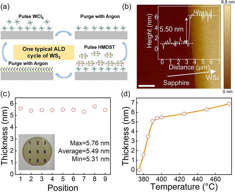 | ||
| Fig. 1 (a) Process diagram of ALD WS2 film. (b) The thickness of WS2 film was deposited with 400 cycles at 400 °C, scalebar: 2 μm. (c) The thickness of the film in different areas on a 2-inch wafer. (d) The thickness of WS2 film grown at different growth temperatures. | ||
3.2 The study of deposition temperature
After obtaining the deposition window, a detailed investigation was performed to clarify the influence of deposition temperature on the quality of WS2. Fig. 2a shows the AFM and XPS results of WS2 films deposited at 400 °C, which presenting excellent flatness with a roughness of only 0.43 nm. Moreover, the grain of WS2 can be observed, and the average grain size of WS2 is about 100 nm. The XPS results show that the films consist of a mixture ratio of 4.2 for W4+ and W6+, and the W4+ and W6+ correspond to WS2 and WS3, indicating the product of deposition is WSX, a mixture of WS2 and WS3. Existence of W6+ is mainly due to the lack of reducing environment during the ALD reaction.34 In Fig. 2b, when the deposition temperature is 425 °C, particles appear on the surface, with the roughness increasing to 0.56 nm. The XPS results show that the ratio of W4+ to W6+ increases slightly to 6.4, indicating that appropriate temperature benefits the reduction of W6+. As shown in Fig. 2c and d, with even higher deposition temperatures, the roughness of the films increases rapidly to 0.82 nm and 1.86 nm, respectively. Also in the conditions of 450 °C and 475 °C, many clumps have appeared in films. And according to the XPS analysis, the W4+/W6+ ratio decreases to 3.2 and 2.4, respectively. This indicates that above 425 °C, the precursor begins to decompose before sufficient reaction, generating large amounts of W6+ that cannot be reduced. Thus, 400–425 °C is the preferred window for film growth, and 400 °C was selected as the optimal growth temperature due to its smoother surface.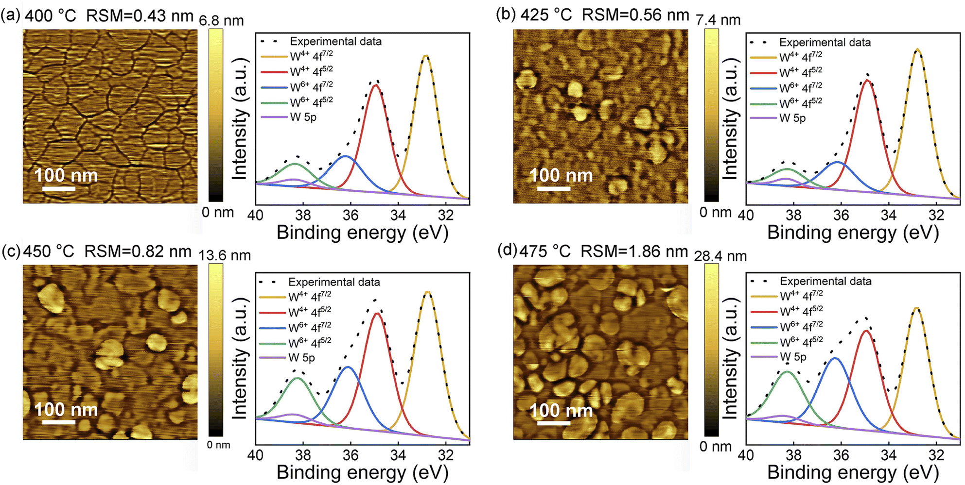 | ||
| Fig. 2 Morphologies characterizations and XPS analysis of WS2 films deposited at different deposition temperatures of (a) 400 °C, (b) 425 °C, (c) 450 °C, and (d) 475 °C, respectively. | ||
3.3 The morphologies and growth mechanism of WS2
In Fig. 3, AFM, high angle annular dark field-scanning transmission electron microscopy (HAADF-STEM) and SEM were applied to demonstrate the morphologies and growth process of WS2. Through AFM, three types of morphologies (non-connected films, flat film, and vertical structure) can be observed corresponding to films with 200, 400, and 600 ALD cycles, respectively. Fig. 3a shows the initial nucleation stage of WS2 films with 200 ALD cycles. At this stage, the size of WS2 varies from tens of nanometers to hundreds of nanometers, and the thickness is about 1.5 nm, corresponding to the thickness of bi-layer WS2 (as shown in Fig. S3†). As shown in Fig. 3b, WS2 with 400 ALD cycles result in the formation of flat films. At this stage, WS2 was in horizontal growth mode, and the non-connected films were connected to form flat films. Fig. 3c shows a HAADF-STEM image of plane-view WS2 film with 600 ALD cycles, a large number of WS2 with nanowire structure were found. At this stage, WS2 is dominated by the vertical growth mode. In Fig. 3d–i, SEM characterizations depict the growth mechanism in more detail. As shown in Fig. 3d and e, WS2 gradually extend from non-connected films (with 200 ALD cycles) to interlinked network (with 300 ALD cycles). This indicates that WS2 at 300 cycles was still insufficient to form a complete film. In Fig. 3f, for 400 cycles, WS2 has formed a uniform film, consistent with results in AFM. WS2 with 200 and 400 ALD cycles correspond to 2 and 5 layers, respectively. So in the initial growth stage, the horizontal growth rate was much higher than the vertical growth, and no warping microstructures was observed. This is because the edge of WS2 performs better precursor adsorption than the base surface, so WS2 is more likely to nucleate along the edge of the film rather than on the film's surface.35 Fig. 3g corresponds to WS2 film with 500 ALD cycles, with visible grains. In this period, an upward warping trend appears at the junction of WS2. This phenomenon can be attributed to the fact that after the island structure connect, the precursor is more likely to adsorb at the grain boundary between adjacent grains. In addition, the strain at grain boundaries will continuously accumulate, which changes the growth direction of WS2.28 As shown in Fig. 3h, for 550 cycles, these warped parts overgrow, and the junction of island nanosheets is covered with vertical WS2. At this stage, the reactive active site of the reaction is warped at the edge, so WS2 grows rapidly along the vertical direction. Fig. 3i shows WS2 films with 600 ALD cycles, where the surface of WS2 has already been covered with dense vertical WS2. It is worth noting that the morphology of WS2 will not change significantly if the ALD cycles continue to increase (as shown in Fig. S4†).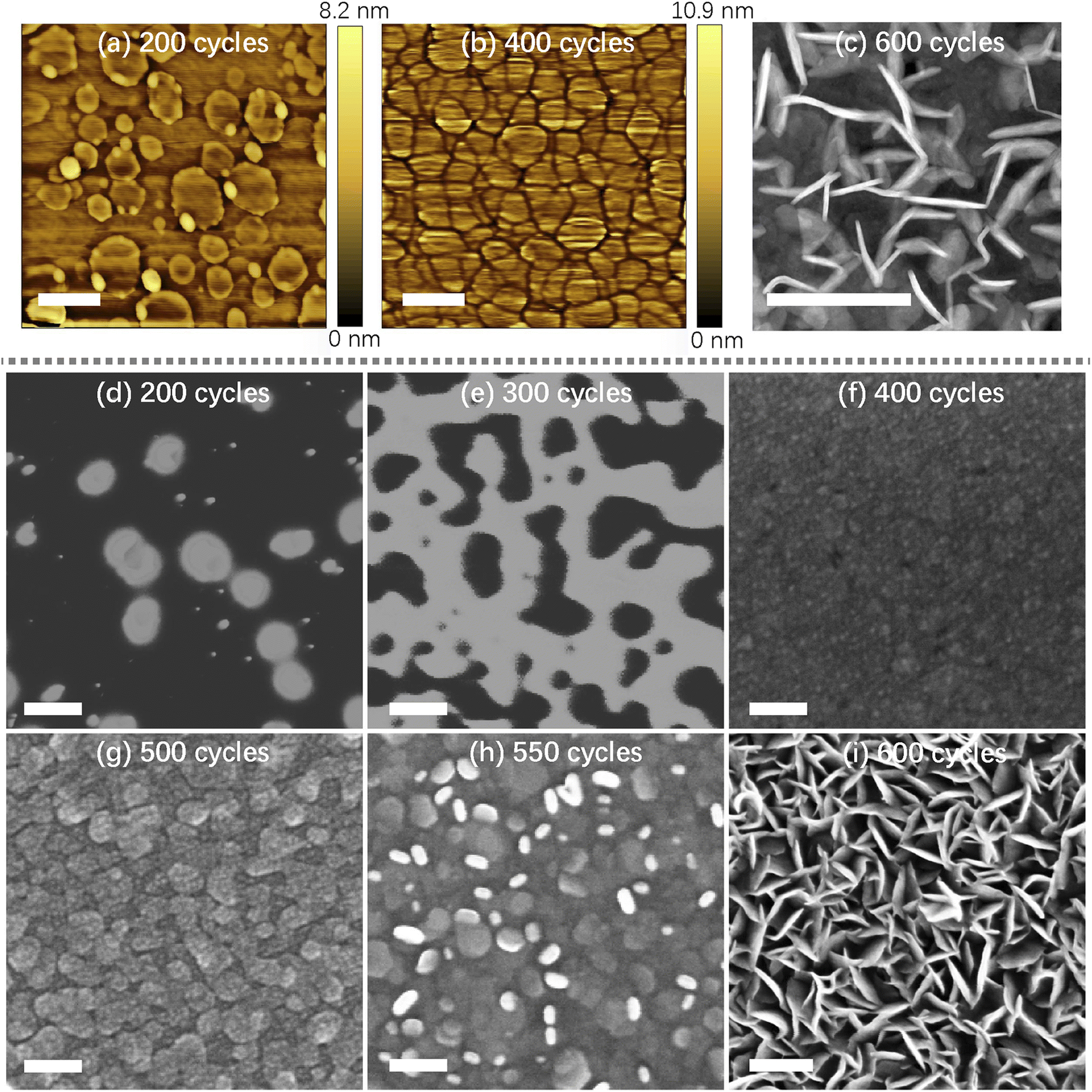 | ||
| Fig. 3 The morphology of WS2 films with different deposition cycles. AFM characterizations of films with (a) 200 and (b) 400 ALD cycles. (c) HAADF-STEM image of plane-view film 600 ALD cycles. (d)–(i) SEM results of samples with different ALD cycles. The scale bars in all figures are 200 nm. | ||
3.4 Annealing and doping process of WS2
Fig. 4 shows a post-annealing process to improve the quality of films in the S atmosphere. Fig. 4a shows the Raman spectra at different annealing temperatures. E12g and A1g represent the in-plane and out-of-plane vibration modes of WS2, respectively.36 With the increase of annealing temperature, the intensity of peak E12g increases significantly, which confirms the film crystallinity can be improved availably by annealing. In Fig. 4b, after 950 °C for 2 hours annealing, the fine spectra of W 4f exhibited only one pair of W 4f5/2 and W 4f7/2 peaks, indicating the W6+ have been reduced to W4+, along with a similar result for S 2p spectra, both without characteristic peaks indicative of W6+–S bonding. After annealing, the stoichiometric ratio of W/S was reduced to 1:2. Fig. 4c shows deposited and annealed TEM of WS2; the average thickness of WS2 film is about 4.7 nm, and the number of layers is 5. Compared to unannealed film, the annealed WS2 film has a more smooth and clear layered structure. It can be demonstrated that post-annealing is critical for WS2 film grown by ALD, which can significantly improve the crystallinity, optimize the proportion of elements and smooth the lamellar structure of the film.
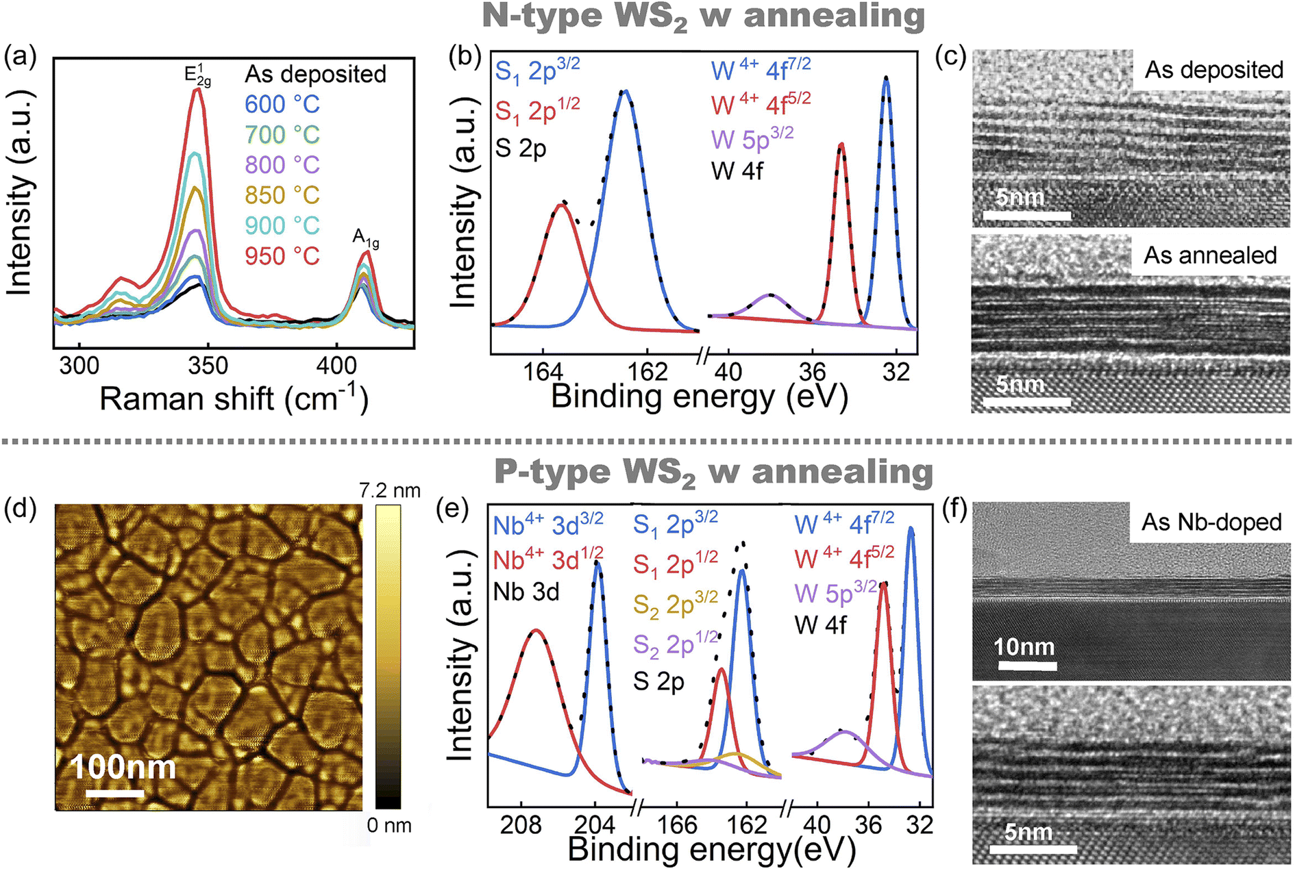 | ||
| Fig. 4 (a) Raman spectra of WS2 at different annealed temperatures. (b) XPS spectra of WS2 at 950 °C annealed temperature. (S1 stands for S2−–W4+ bonding) (c) the cross-sectional TEM results for deposited and annealed WS2 film. (d) AFM, (e) XPS (S2 stands for S2−–Nb4+ bonding), and (f) TEM of Nb-doped WS2 film. | ||
ALD can accurately dope WS2 films by introducing doping precursors.37 Nb-doped WS2 has been proved that the acceptor energy level appears at the top of the valence band of WS2, which can achieve P-type semiconductor characteristics.38 In addition, compared with other elements, Nb substituted W has lower formation energy and slight local distortion, and Nb can remain stable through covalent bonds within the lattice.39 WS2 is natively an N-type, which origin is existence of native sulfur vacancies provided omnipresent electron donating. When Nb with five valence electrons replaces W with six valence electrons, one electron is removed from the system to keep the total charge neutrality, causing the top valence band becomes electron deficient, and the system becomes hole-rich and P-doped.40 Therefore, Nb is a suitable doping element for preparing P-type WS2 films. Nb doping can be easily controlled by programming ALD deposition process. Next, NbCl5 is added to the WS2 process as a doping precursor for preparing P-type WS2 film (detailed doping process in Fig. S5†). The annealing process of P- type WS2 is the same as that of N-type WS2. Fig. 4d shows the AFM image of Nb-doped WS2, with a roughness of 0.48 nm, which is not distinguishable from the undoped WS2 film. This indicates that Nb doping will not break the surface smoothness of WS2 films. In Fig. 4e, XPS proves the existence of Nb in P-type WS2. A fine spectrum can prove that Nb is doped into WS2 as Nb4+. W 4f fine spectrum in P-type WS2 also only demonstrate a pair of characteristic peaks W4+ 4f7/2 and W4+ 4f5/2, which is consistent with N-type WS2. The difference is in the fine spectrum of S, in addition to the characteristic peaks of W–S, the characteristic peaks of Nb–S are also observed, indicating that both Nb4+ and W4+ are bonded to S2−. Fig. 4f shows the TEM of Nb-doped WS2 film, compared with undoped WS2 thin films, Nb doping does not significantly damage the original flat layered structure. The results indicate that Nb is a non-destructive effective doping for ALD-grown WS2.
3.5 Functionalized device applications
The in-plane conductivity of WS2 is 8–70 times that of the out-of-plane direction.41 So flat WS2 film can be used as a functional material for FETs, and vertical WS2 is more suitable for preparing gas sensors because the vertical structure can provide more abundant morphology and expose more adsorption sites.42 As shown in Fig. 5a, we selected flat film to prepare the FET array. Fig. 5b shows the transfer characteristic of the N- and P-type FET based on WS2 film at VDS = 0.5 V. The devices show typical N and P type transfer characteristic before and after Nb-doped, respectively. The red dash line shows the N-FETs transfer curve under 800 °C annealed. Compared with 950 °C annealed devices, although the devices exhibit N- type FET characteristics, the Ion is reduced by two orders of magnitude, with a Ion/Ioff ratio of only 102. The poor performance can be attributed to the low crystallinity of WS2 annealed at 800 °C, and there is still defects in WS2 film. For 950 °C annealed N-FET, the μFE is 7.25 cm2 V−1 s−1, and the Ion/Ioff is above 105. And for P-FET, the μFE is 0.23 cm2 V−1 s−1, and the Ion/Ioff is above 102. In Fig. 5c and d, without Nb-doped WS2 FETs show typical N-type output characteristic, and Nb-doped WS2 FETs show typical P-type output characteristic. The current tends to saturate at VDS = 5 V. This indicates that the carrier type of WS2 FETs can indeed be changed from electron to hole by Nb doping.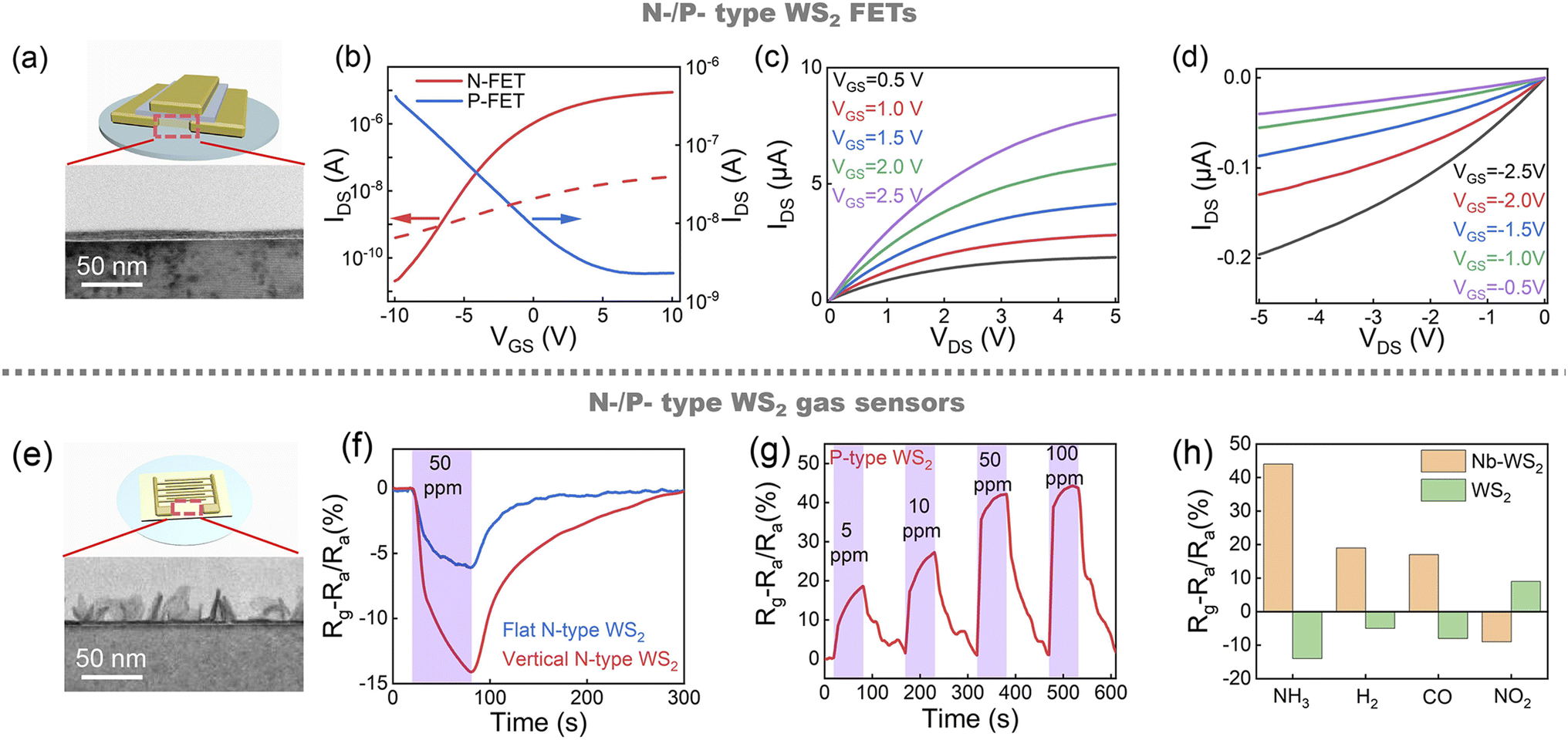 | ||
| Fig. 5 (a) Schematic illustration of top-gated WS2 FET on a sapphire substrate. (b) Transfer characteristics of N-type and P-type WS2 FETs at VDS = 0.5 V. Output characteristics of (c) N-type and (d) P-type WS2 FETs. (e) Schematic illustration of WS2 gas sensor. (f) Response to NH3 exposure of flat and vertical WS2 gas sensors. (g) Response to NH3 exposure of vertical P-type WS2 gas sensors. (h) Selectivity of vertical N- and P-type WS2 gas sensors upon exposure to various gases (50 ppm NH3, H2, CO, and NO2, respectively). | ||
Fig. 5e shows a schematic of a gas sensor. In Fig. 5f, the response of horizontal and vertical N-type WS2 and Nb-doped P-type WS2 to NH3 at room temperature was measured, respectively. The gas response was calculated according to the following relation: ΔR/Ra = (Rg − Ra)/Ra, where Ra and Rg are the resistances of the sensing devices to the air and analyte gases, respectively. The response of flat and vertical N-type WS2 is 6% and 14%, respectively. Nb-doped nanomaterials have been proven to be a promising method for improving gas sensing performance.43 In Fig. 5g, to further demonstrate highly enhanced gas response properties in Nb-doped WS2 film, resistance variations of P-type films to diluted NH3 (5–100 ppm) gas are measured. The P-type vertical WS2 gas sensor shows a significantly high response (42%) to 50 ppm NH3 exposure at room temperature. Fig. 5h shows the comparative response to various gases. For P-type WS2, a positive response was shown upon NH3, H2, or CO exposure, while a negative response occurred with exposure to NO2. The response of N-type WS2 is opposite to that of P-type WS2. This is related to the different adsorption energy and degree of charge transfer to various gases.44 It is also very evident that the NH3 response is much higher than other gases.
4. Conclusions
In this work, we demonstrate ALD-WS2 processes during which morphologies and doping type can be flexibly regulated based on different requirements for various device applications. First, by studying the deposition temperature, growth mechanism, and annealing conditions of WS2 deposited by ALD, high-quality wafer-scale N-type WS2 films were prepared. Then, ALD can excellently regulate the morphologies and Nb-doping to obtain ideal P-type WS2 films. Finally, we successfully prepared high-performance N-type and P-type FETs with flat WS2 film and prepared N-type and P-type gas sensors with vertical WS2. Nb doping can regulate carrier types and significantly improve the response of gas sensors. The results show that morphologies and doping type of WS2 films can be regulated simply by adjusting and programming the ALD processes, and can be well applied to FETs and gas sensors.Author contributions
The manuscript was written through contributions of all authors. All the authors have given approval to the final version of the manuscript.Conflicts of interest
There are no conflicts to declare.Acknowledgements
This work is partially supported by NSFC (62004044 and 62204048). L. J. acknowledges the support of the starting research fund from Fudan University and the support by State Key Laboratory of ASIC & System (2021MS004).Notes and references
- J. Shim, H. Y. Park, D. H. Kang, J. O. Kim, S. H. Jo, Y. Park and J. H. Park, Adv. Electron. Mater., 2017, 3, 1600364 CrossRef.
- X. Wang, J. Song and J. Qu, Angew. Chem., Int. Ed., 2019, 58, 1574 CrossRef CAS PubMed.
- C. Xie, C. Mak, X. Tao and F. Yan, Adv. Funct. Mater., 2017, 27, 1603886 CrossRef.
- S. Y. Kim, J. Kwak, C. V. Ciobanu and S. Y. Kwon, Adv. Mater., 2019, 31, 1804939 CrossRef PubMed.
- G. H. Park, K. Nielsch and A. Thomas, Adv. Mater. Interfaces, 2019, 6, 1800688 CrossRef.
- K. F. Mak and j. Shan, Nat. Photonics, 2016, 10, 216 CrossRef CAS.
- W. Choi, N. Choudhary, G. H. Han, J. Park, D. Akinwande and Y. H. Lee, Mater. Today, 2017, 20, 3 CrossRef.
- A. B. Kaul, J. Mater. Res., 2014, 29, 348 CrossRef CAS.
- C. Lan, C. Li, J. C. Ho and Y. Liu, Adv. Electron. Mater., 2021, 7, 2000688 CrossRef CAS.
- W. Zhang, Z. Huang, W. Zhang and Y. Li, Nano Res., 2014, 7, 1731 CrossRef CAS.
- Z. Ye, T. Cao, K. O’brien, H. Zhu, X. Yin, Y. Wang, S. G. Louie and X. Zhang, Nature, 2014, 513, 214 CrossRef CAS PubMed.
- Z. Y. Zhu, Y. C. Cheng and U. Schwingenschlögl, Phys. Rev. B: Condens. Matter Mater. Phys., 2011, 84, 153402 CrossRef.
- W. Zhao, Z. Ghorannevis, L. Chu, M. Toh, C. Kloc, P. H. Tan and G. Eda, ACS Nano, 2013, 7, 791 CrossRef CAS PubMed.
- Y. G. You, D. H. Shin, J. H. Ryu, E. E. B. Campbell, H. J. Chung and S. H. Jhang, Nanotechnology, 2021, 32, 505702 CrossRef CAS PubMed.
- A. Rawat, N. Jena and A. D. Sarkar, J. Mater. Chem. A, 2018, 6, 8693 RSC.
- M. W. Iqbal, K. Shahzad, G. Hussain, M. K. Arshad, R. Akbar, S. Azam, S. Aftab, T. Alharbi and A. Majid, Mater. Res. Express, 2019, 6, 115909 CrossRef CAS.
- S. Tongay, W. Fan, J. Kang, J. Park, U. Koldemir, J. Suh, D. S. Narang, K. Liu, J. Ji and J. Li, Nano Lett., 2014, 14, 3185 CrossRef CAS PubMed.
- P. Bhattacharyya and D. Acharyya, IEEE Sens. J., 2021, 21, 22414 CAS.
- A. Sebastian, R. Pendurthi, T. H. Choudhury, J. M. Redwing and S. Das, Nat. Commun., 2021, 12, 693 CrossRef CAS PubMed.
- Y. Wan, E. Li, Z. Yu, J. K. Huang, M. Y. Li, A. S. Chou, Y. T. Lee, C. J. Lee, H. C. Hsu, Q. Zhan, A. Aljarb, J. H. Fu, S. P. Chiu, X. Wang, J. J. Lin, Y. P. Chiu, W. H. Chang, H. Wang, Y. Shi, N. Lin, Y. Cheng, V. Tung and L. J. Li, Nat. Commun., 2022, 13, 4119 CrossRef PubMed.
- W. T. Koo, J. H. Cha, J. W. Jung, S. J. Choi, J. S. Jang, D. H. Kim and I. D. Kim, Adv. Funct. Mater., 2018, 28, 1802575 CrossRef.
- H. Tang, Y. Li, R. Sokolovskij, L. Sacco, H. Zheng, H. Ye, H. Yu, X. Fan, H. Tian, T. L. Ren and G. Zhang, ACS Appl. Mater. Interfaces, 2019, 11, 40850–40859 CrossRef CAS PubMed.
- W. Gao, S. Zhang, F. Zhang, P. Wen, L. Zhang, Y. Sun, H. Chen, Z. Zheng, M. Yang, D. Luo, N. Huo and J. Li, Adv. Electron. Mater., 2021, 7, 2000964 CrossRef CAS.
- J. Gu, B. Chakraborty, M. Khatoniar and V. M. Menon, Nat. Nanotechnol., 2019, 14, 1024 CrossRef CAS PubMed.
- T. Nam, S. Seo and H. Kim, J. Vac. Sci. Technol., 2020, 38, 030803 CrossRef CAS.
- S. W. Nam, M. J. Rooks, K. B. Kim and S. M. Rossnagel, Nano Lett., 2009, 9, 2044 CrossRef CAS PubMed.
- N. Wei, N. Gao, H. Xu, Z. Liu, L. Gao, H. Jiang, Y. Tian, Y. Chen, X. Du and L. M. Peng, Nano Res., 2022, 15, 9876 Search PubMed.
- H. Yang, Y. Wang, X. Zou, R. X. Bai, S. Han, Z. Wu, Q. Han, Y. Zhang, H. Zhu, L. Chen, X. Lu, Q. Sun, J. C. Lee, E. T. Yu, D. Akinwande and L. Ji, ACS Appl. Mater. Interfaces, 2021, 13, 43115 CrossRef CAS PubMed.
- H. Yang, Y. Wang, X. Zou, R. Bai, Z. Wu, S. Han, T. Chen, S. Hu, L. Chen, D. W. Zhang, J. C. Lee, X. Lu, P. Zhou, Q. Sun, E. T. Yu, D. Akinwande and L. Ji, Research, 2021, 9862483 CAS.
- B. Groven, A. N. Mehta, H. Bender, J. Meersschaut, T. Nuytten, P. Verdonck, T. Conard, Q. Smets, T. Schram, B. Schoenaers, A. Stesmans, V. Afanaśev, W. Vandervorst, M. Heyns, M. Caymax, I. Radu and A. Delabie, Chem. Mater., 2018, 30, 7648 CrossRef CAS.
- Y. Jang, S. Yeo, H. B. R. Lee, H. Kim and S. H. Kim, Appl. Surf. Sci., 2016, 365, 160 CrossRef CAS.
- Y. Huang, L. Liu, J. Sha and Y. Chen, Appl. Phys. Lett., 2017, 111, 063902 CrossRef.
- M. Chhowalla, H. S. Shin, G. Eda, L. J. Li, K. P. Loh and H. Zhang, Nat. Chem., 2013, 5, 263 CrossRef PubMed.
- Y. Wu, M. H. Raza, Y. C. Chen, P. Amsalem, S. Wahl, K. Skrodczky, X. Xu, K. S. Lokare, M. Zhukush, P. Gaval, N. Koch, E. A. Quadrell and N. Pinna, Chem. Mater., 2019, 31, 1881 CrossRef CAS.
- S. Balasubramanyam, M. Shirazi, M. A. Bloodgood, L. Wu, M. A. Verheijen, V. Vandalon, W. M. M. Kessels, J. P. Hofmann and A. A. Bol, Chem. Mater., 2019, 31, 5104 CrossRef CAS PubMed.
- X. Huang, Y. Gao, T. Yang, W. Ren, H. M. Cheng and T. Lai, Sci. Rep., 2016, 6, 1 CrossRef PubMed.
- V. Vandalon, M. Verheijen, W. Kessels and A. Bol, ACS Appl. Nano Mater., 2020, 3, 10200 CrossRef CAS PubMed.
- Y. Jin, Z. Zeng, Z. Xu, Y. C. Lin, K. Bi, G. Shao, T. S. Hu, S. Wang, S. Li, K. Suenaga, H. Duan and Y. Feng, Chem. Mater., 2019, 31, 3534 CrossRef CAS.
- N. Li, Z. Liu, S. Hu and H. Wang, Solid State Commun., 2018, 269, 58 CrossRef CAS.
- J. Gao, Y. D. Kim, L. B. Liang, J. C. Idrobo, P. Chow, J. Tan, B. Li, L. Li, B. G. Sumpter, T. M. Lu, V. Meunier, J. Hone and N. Koratkar, Adv. Mater., 2016, 28, 9735 CrossRef CAS PubMed.
- A. Pisoni, J. Jacimovic, R. Gaál, B. Náfrádi, H. Berger, Z. Révay and L. Forró, Scr. Mater., 2016, 114, 48 CrossRef CAS.
- S. Y. Cho, S. J. Kim, Y. Lee, J. S. Kim, W. B. Jung, H. W. Yoo, J. Kim and H. T. Jung, ACS Nano, 2015, 9, 9314 CrossRef PubMed.
- S. Y. Cho, Y. Kim, H. S. Chung, A. R. Kim, J. D. Kwon, J. Park, Y. L. Kim, S. H. Kwon, M. G. Hahm and B. Cho, ACS Appl. Mater. Interfaces, 2017, 9, 3817 CrossRef PubMed.
- B. Cho, M. G. Hahm, M. Choi, J. Yoon, A. R. Kim, Y.-J. Lee, S.-G. Park, J.-D. Kwon, C. S. Kim, M. Song, Y. Jeong, K.-S. Nam, S. Lee, T. J. Yoo, C. G. Kang, B. H. Lee, H. C. Ko, P. M. Ajayan and D.-H. Kim, Sci. Rep., 2015, 5, 8052 CrossRef CAS PubMed.
Footnote |
| † Electronic supplementary information (ESI) available. See DOI: https://doi.org/10.1039/d3ra00933e |
| This journal is © The Royal Society of Chemistry 2023 |