DOI:
10.1039/D2RA08278K
(Paper)
RSC Adv., 2023,
13, 5885-5892
Searching for d0 spintronic materials: bismuthene monolayer doped with IVA-group atoms†
Received
28th December 2022
, Accepted 11th February 2023
First published on 17th February 2023
Abstract
Doping with non-metal atoms may endow two-dimensional (2D) materials with feature-rich electronic and magnetic properties to be applied in spintronic devices. In this work, the effects of IVA-group (C, Si, and Ge) atom doping on the structural, electronic and magnetic properties of bismuthene monolayer are investigated by means of first-principles calculations. Pristine monolayer is a direct gap semiconductor with band gap of 0.56 eV, exhibiting Rashba splitting caused by spin–orbit coupling. Regardless doping level, C and Si incorporation leads to the emergence of significant magnetism, which is generated mainly by the dopants as demonstrated by the spin density illustration. Depending on the dopant nature and concentration, either half-metallic or magnetic semiconductor characters can be induced by doping, which are suitable to generate spin current in spintronic devices. Further study indicates an energetically favorable antiferromagnetic coupling in the C- and Si-doped systems, suggesting the predominant Pauli repulsion over Coulomb repulsion. Meanwhile, bismuthene monolayer is metallized by doping Ge atoms. Magnetization occurs with 12.5% and 5.56% of Ge atoms, meanwhile the non-magnetic nature is preserved under lower doping level of 3.125%. Results presented herein may introduce C and Si doping as efficient approach to functionalize non-magnetic bismuthene monolayer, enriching the family of 2D d0 magnetic materials for spintronic applications.
I. Introduction
Stimulated by the success of graphene and its derivatives,1–3 researchers have devoted great efforts in designing and developing new two-dimensional (2D) materials with novel properties.4–6 Between them, bismuthene – 2D structure of bismuth – has received particular attention, being synthesized successfully in experiments. For example, a combined theoretical and experimental investigation of bismuthene grown on SiC(0001) substrate has been carried out by Reis et al.,7 which demonstrates a quantum spin Hall wide energy gap scenario. Large-scale free-standing bismuthene has been prepared by Yang et al.8 As-synthesized material shows high catalytic performance for the electroreduction reaction of CO2. Similarly, bismuthene nanosheets prepared by Ma et al.9 exhibit a rapid kinetics for electrochemical reduction of CO2 to formate, where the catalysts preferentially promote fast reaction towards HCOO*. High-quality few-layer bismuthene (FLB) with ultra-large lateral dimensions, areas up to 30 μm2, and a few nanometers of thickness has been successfully prepared by Torres et al.10 in good yield. High conductivity and excellent electrical properties make FLB promising candidate for adenine dinucleotide (NADH) sensing.
On the other hands, several research groups have realized theoretical studies to get deep insights into fundamental properties of bismuthene monolayer. Kecik et al.11 have investigated the optoelectronic properties of antimonene, bismuthene monolayer and their compound. Results show the indirect gap semiconductor nature of bismuthene monolayer with an energy gap of 0.51 eV, consequently, it exhibits a strong optical absorption in infrared region. Strain-dependent electronic and thermoelectric properties of bismuthene monolayer has been studied by Radha et al.12 using density functional theory (DFT) calculations combined with semiclassical Boltzmann transport theory. It is observed a semiconductor-to-metallic behavior transition at tensile strain of 8% and compressive strain of −6%. Sun et al.13 have demonstrated that the optical properties of bismuthene monolayer and bilayer in mid-infrared regime may be significantly enhanced by properly applying biaxial and vertical strains, as well as creating vacancies. Because of its simplicity and effectiveness, doping has been investigated to induce novel features in bismuthene monolayer. Qi et al.14 have shown that 3d transition metal doping may magnetize bismuthene single layer, where different electronic behaviors as spin-polarized semiconductor (doped with Cr), magnetic metal (doped with V), and half-metallic (doped with Mn and Fe) are obtained. Bismuthene monolayers doped with 4d transition metals (Cr, Nb, Tc, and Ru) as promising candidates for spintronic applications have been introduced by Muhammad et al.15
Revising the literature, it has been found new approach to develop new 2D materials for possible spintronic applications by simply doping with non-metal atoms.16,17 In this work, the effects of doping with IVA-group atoms (C, Si, and Ge) on the bismuthene monolayer electronic and magnetic properties are systematically investigated. These strategies are expected to induce novel features in a non-magnetic bismuthene single layer. Effects are analyzed through changes and modifications of the local structure, band structure, projected density of states, spin density and Bader charge analysis. The effects of doping level are also examined by considering dopant concentration of 12.5%, 5.56%, and 3.125%. Results demonstrate high effectiveness of doping approach to functionalize bismuthene monolayer for spintronic applications. In addition, the C- and Si-co-doped induces the half-metallicity. Meanwhile [C and Ge] and [Si and Ge] codoping preserves the non-magnetic nature of bismuthene monolayer (see Fig. S1 and S2 of the ESI file†).
II. Computational details
Density functional theory (DFT) method18 – implemented in Vienna ab initio Simulation Package (VASP)19,20 – has been employed to examine the effects of IVA-group atoms (C, Si, and Ge) doping on bismuthene monolayer electronic and magnetic properties. Perdew–Burke–Ernzerhof generalized gradient approximation (GGA-PBE)21 is adopted to calculate the electron exchange–correlation energies, while the electron–ion interactions are described by projector-augmented wave (PAW) pseudopotentials. The expansion of electronic states is realized with an energy cutoff of 500 eV. First Brillouin zone is sampled with a Monkhorst–Pack mesh22 of 4 × 4 × 1. Energy and force convergences are set to 10−5 eV and 0.01 eV Å−1, respectively. A vacuum space as large as 14 Å guarantees the creation of monolayer without interactions between consecutive slabs.
III. Results and discussion
A. Pristine bismuthene monolayer
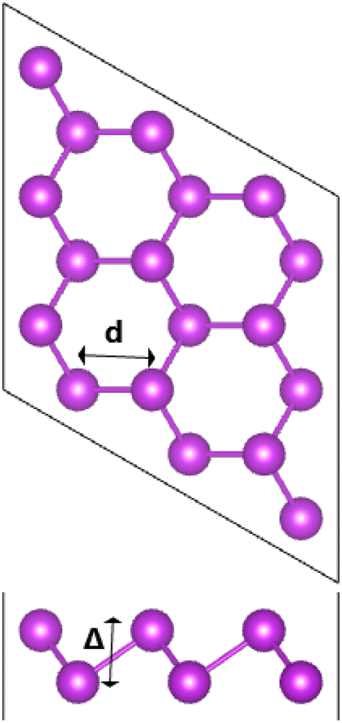
Fig. 1 shows a 3 × 3 × 1 supercell of bismuthene monolayer. The optimized structure can be fully described by following parameters: (1) lattice parameter a of 4.33 (Å); (2) buckling height ΔBi–Bi of 1.73 (Å); (3) interatomic angle ∠BiBiBi of 90.700; and (4) chemical bond length dBi–Bi of 3.05 (Å). Fig. 2a shows the band structure (BS) of bismuthene monolayer calculated along Γ − M − K − Γ high symmetry direction. BS profile indicates the direct gap semiconductor nature considering both valence band maximum and conduction band minimum at same Γ point. Our simulations yield a band gap of 0.56 eV. Since bismuth is a heavy atom, the spin–orbit coupling (SOC) may play important role in the bismuthene electronic properties. It can be noted the Rashba-type splitting, where the valence band maximum shifts from Γ point to ΓM and ΓK directions decreasing slightly the energy gap to 0.49 eV. Further insights into the BS formation are achieved through projected density of states (PDOS) (see Fig. 2b). Note that Bi-6p orbital (px, py, and pz states) is the main contributor in the considered energy range from −3 to 3 eV. All these results are in good agreement with previous calculations,23 suggesting the reliability of the employed computational parameters. It is worth mentioning that in a buckled structure, bismuthene may exhibit a mix of sp2 and sp3 hybridization, giving place to the formation of strong σ bonds and weak π bonds, respectively. Consequently, chemical bonds are predominantly covalent as a result of the strong electronic hybridization, which is a characteristic of elemental 2D materials.23,24
 |
| | Fig. 1 A 3 × 3 × 1 supercell of bismuthene monolayer. | |
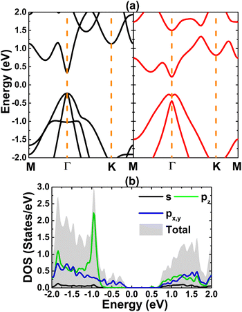 |
| | Fig. 2 (a) Electronic band structure (PBE: black curve; PBE + SOC: red curve) and (b) density of states of bismuthene monolayer. | |
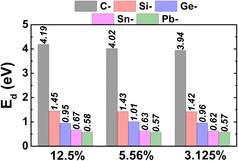
To study the doping effects, different doping levels of 12.5%, 5.55%, and 3.125% are considered, which are created by replacing one Bi atom by one IV-group atom in a 2 × 2 × 1 (Bi7C), 3 × 3 × 1 (Bi17C), and 4 × 4 × 1 (Bi31C) supercell, respectively. The generation of different supercell sizes conducts to a homogeneous distribution of impurities. The doping energy Ed is calculated as follows:
| | |
Ed = Edt − Emt + μB − μX
| (1) |
where
Edt and
Emt are total energy of the doped and pristine system, respectively;
μBi and
μX denote chemical potential of Bi and X (X = C, Si, Ge, Sn, and Pb) atom, respectively. Results are given in
Table 1 and illustrated in
Fig. 3. Note that this parameter decreases according to increase the atomic number of IVA-group atom, which may be derived from the atomic size. Larger atomic radius of dopant, smaller will be difference in atomic size (in comparison with host Bi atom).
Table 1 Bond length dX–Bi (Å) and buckling height ΔX–Bi (Å) between dopants and their first neighbor, doping energy Ed (eV), Charge transfer of dopant ΔQ (e; “+”: charge losing; “−”: charge gaining), and total magnetic moment μt (μB) of the C-, Si-, and Ge-doped bismuthene monolayer
| |
dX–Bi |
ΔX–Bi |
Ed |
ΔQ |
μt |
| C-Doped |
| 12.5% |
2.29 |
0.58 |
4.19 |
−0.92 |
0.23 |
| 5.56% |
2.28 |
0.55 |
4.02 |
−0.92 |
0.97 |
| 3.125% |
2.28 |
0.56 |
3.94 |
−0.92 |
1.00 |
![[thin space (1/6-em)]](https://www.rsc.org/images/entities/char_2009.gif) |
| Si-Doped |
| 12.5% |
2.74 |
1.06 |
1.45 |
−0.12 |
0.99 |
| 5.56% |
2.74 |
1.11 |
1.43 |
−0.12 |
1.00 |
| 3.125% |
2.73 |
1.11 |
1.42 |
−0.11 |
1.00 |
|
| Ge-Doped |
| 12.5% |
2.81 |
1.10 |
0.95 |
−0.10 |
0.60 |
| 5.56% |
2.87 |
1.59 |
1.01 |
−0.09 |
0.44 |
| 3.125% |
2.90 |
1.79 |
0.96 |
−0.10 |
0.00 |
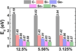 |
| | Fig. 3 Doping energy of the C-, Si-, Ge-, Sn-, and Pb-doped bismuthene monolayer with different doping levels. | |
As mentioned above, our main aim is to search for new 2D magnetic materials. It is anticipated that Sn and Pb doping induces non magnetism in the bismuthene monolayer (see Fig. S3 and S4 of the ESI file†). Therefore, further analysis of results is realized only for the cases of C, Si, and Ge doping.
B. C-Doped bismuthene monolayer
Herein, the C-doped bismuthene monolayer is considered. Firstly, the structure is relaxed to find out the equilibrium state. Due to the difference in atomic size, the substitutional incorporation of C atom causes a significant local distortion, which is characterized by the structural parameters listed in Table 1. Note that the interatomic distance between dopant and its neighbor decreases significantly (about 25% from original value of 3.05 Å), suggesting a local tension. Moreover, a significant reduction of the buckling height (about 66% to 68% from original value of 1.73 Å) indicates an inward movement of C dopant. Undoubted that these results are derived from a considerably smaller atomic size of C atom as compared to Bi atom.
Fig. 4 shows the spin-polarized band structures (BSs) of the C-doped systems. It can be noted the spin-asymmetry, mostly around the Fermi level. The degree of spin asymmetry increases according to decrease the doping level. BSs profile indicates the metallic character of Bi7C monolayer since its electronic states overlap with the Fermi level in both spin channels. Meanwhile, feature-rich electronic natures are obtained in the Bi17C and Bi31C monolayers, which are determined by new middle-gap states. Specifically, the former exhibits half-metallic character generated by a semiconductor spin-up state (with an indirect band gap of 0.40 eV) and a metallic spin-down state. Unlikely, the movement of spin-down new electronic state to conduction band leads to the emergence of the magnetic semiconductor in latter system. This is a result of the spin-up indirect band gap of 0.55 eV and spin-down direct band gap of 0.26 eV, respectively. Results may suggest the C doping as efficient approach to functionalize bismuthene monolayer for spintronic applications, considering that half-metallic and magnetic semiconductor characters are expected in spintronic materials to generate spin current.3,25,26 To further analyze the BS formation, the orbital-decomposed density of states (DOS) of C dopant and its first and second Bi neighbor are displayed in Fig. 5. It is worth mentioning that there is no significant changes of electronic interactions in regions far away from the doping site, therefore atomic DOS spectra are quite similar to those in pristine monolayer discussed above. From the figure, one can see that Bi atoms keep their dominant role in forming the lower part of valence band and upper part of conduction band. Meanwhile the middle-gap electronic states are built mainly by C-pz state in both spin configurations, which determines mainly the ground-state properties of the doped systems. The appearance of C-pz state to construct the upper part of valence band may suggest a charge gaining from host monolayer. This feature is demonstrated by the Bader charge analysis, which indicates the charge transfer process of 0.92 e. Therefore, C–Bi chemical bonds are predominantly ionic, in agreement with the insignificant electronic hybridization observed in Fig. 5.
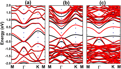 |
| | Fig. 4 Electronic band structure (spin-up: black curve; spin-down: red curve; the Fermi level is set to 0 eV) of the C-doped bismuthene monolayer with doping level of (a) 12.5%, (b) 5.56%, and (c) 3.125%. | |
 |
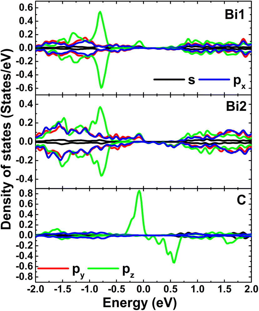
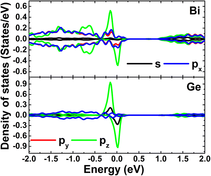
| | Fig. 5 Projected density of C dopant and its first (Bi1) and second (Bi2) Bi neighbor (the Fermi level is set to 0 eV) of the C-doped bismuthene monolayer with doping level of 5.56%. | |
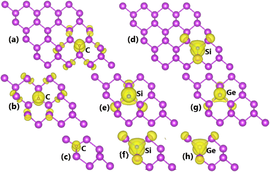
The spin-unbalanced band structures may give signal of important magnetization of bismuthene monolayer induced by C doping. According to our calculations, total magnetic moments of 0.23, 0.97, and 1.00 (μB) are obtained with dopant concentration of 12.5%, 5.56%, and 3.125%, respectively. The increase of this parameter indicates that the magnetization becomes stronger upon decreasing the doping level, consistent with the degree of spin polarization observed in the band structures. To get more insights, the spin density is illustrated in Fig. 6a–c. Note that C atom originates mainly the magnetic properties, where small contribution is also observed from its first Bi atom. Recalling the DOS spectra, one can attribute the emergence of magnetism to pz state.
 |
| | Fig. 6 Spin density (spin-up: yellow surface; iso-surface value: 0.001) of (a–c) C-, (d–f) Si-, and (g and h) Ge-doped bismuthene monolayer with doping level of 3.125% (first row), 5.56% (second row), and 12.5% (third row). | |
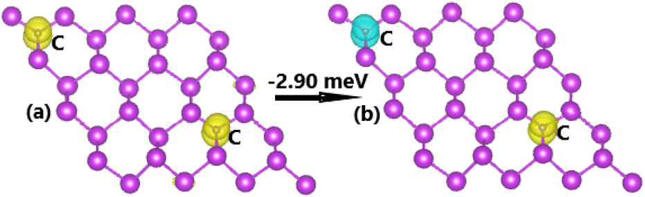
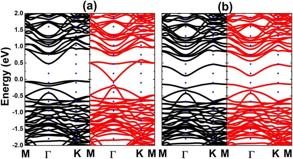
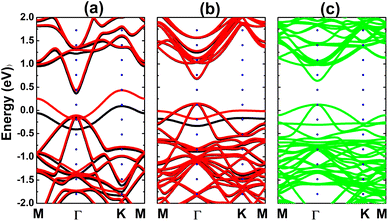
Now, the spin coupling is determined by considering either parallel (ferromagnetic – FM) ordering and antiparallel (antiferromagnetic – AFM) ordering, which are illustrated in Fig. 7 with the calculated energy of magnetic phase transition. Note that AFM state is energetically favorable with an energy of 2.90 meV smaller than FM state. The emergence of AFM state is a result of the Pauli repulsion felt by C-pz electrons, where two electrons can not occupy a same quantum state conducting to an antiparallel spin ordering. The calculated BS of each magnetic state are given in Fig. 8. The ferromagnetic half-metallicity and antiferromagnetic semiconducting are obtained. The first one is generated by semiconductor spin-up state (indirect gap of 0.52 eV) and metallic spin-down state. Meanwhile, a total magnetic moment of 0 μB is reflected in the spin-asymmetric BS of AFM state, where both spin configurations exhibit indirect band gap of 0.24 eV.
 |
| | Fig. 7 Spin ordering in the C-doped bismuthene monolayer (spin-up: yellow surface; spin-down: cyan surface; iso-surface value: 0.002). | |
 |
| | Fig. 8 Electronic band structure (spin-up: black curve; spin-down: red curve) of the C-doped bismuthene monolayer with (a) ferromagnetic and (b) antiferromagnetic ordering. | |
C. Si-doped bismuthene monolayer
Similarly, structural local distortion is also caused by Si incorporation in Bi site. This is reflected in the chemical bond length dSi–Bi and buckling height ΔSi–Bi as listed in Table 1, which exhibit reduction of the order of about 10% and 36 ÷ 38% from their corresponding original values, respectively. Note that the variations are smaller than previous cases of C doping, derived from a larger atomic size of Si atom in comparison with C atom (closer to that of Bi atom).
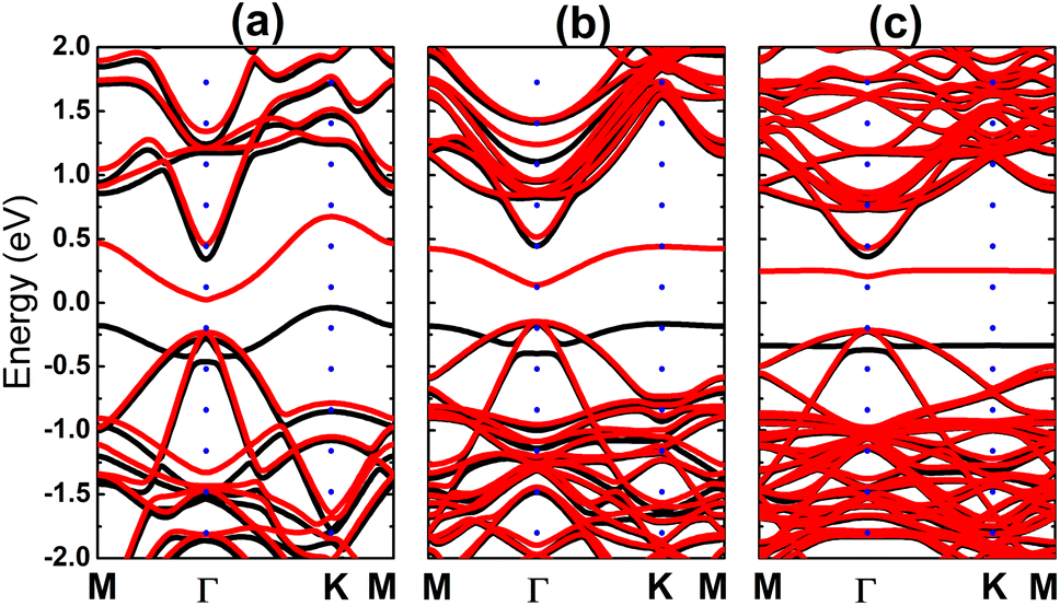
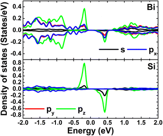
Fig. 9 shows the spin-polarized band structures of the Si-doped bismuthene in different supercell sizes. Independent of the doping level, new energy branches appear in the spin-up valence band and spin-down conduction band, giving place to the spin-asymmetry at the vicinity of the Fermi level. Note that these curves becomes flatter when increasing the supercell size, indicating significant short-term dopant interactions. According to our simulations, indirect band gap of 0.38, 0.61, and 0.60 eV are obtained in the spin-up configuration of Bi7C, Bi17C, and Bi31C monolayer, respectively. While the flat branches in the lower part of conduction band decrease the spin-down energy gap to 0.25, 0.29, and 0.42 eV, respectively. These results indicate the magnetic semiconductor character of bismuthene monolayer induced by Si doping, which may be utilized to generate spin current in spintronic devices by spin filtering.27 In Fig. 10, the orbital-decomposed DOS spectra of Si dopant and its first neighbor Bi atom are given. It is worth mentioning that DOS spectra of second neighbor are not considered herein due to their insignificant changes as compared to those in bare monolayer. The host Bi atoms plays a key role in the energy regions far away from the Fermi level, meanwhile the presence of Si dopant is observed mainly around the Fermi level. Specifically, the middle-gap flat energy branches are formed mainly by Si-pz state, which exhibits also the hybridization with the Bi-pz state. The hybridization leads to a smaller charge gaining. The Bader charge analysis indicates that a quantity of only 0.11 ÷ 0.12 e is transferred from the host monolayer to Si atom, which is quite smaller than those gained by C atom. This may be due to the smaller electronegativity of Si atom as compared to C atom (closer to that of Bi atom).
 |
| | Fig. 9 Electronic band structure (spin-up: black curve; spin-down: red curve; the Fermi level is set to 0 eV) of the Si-doped bismuthene monolayer with doping level of (a) 12.5%, (b) 5.56%, and (c) 3.125%. | |
 |
| | Fig. 10 Projected density of Si dopant and its first Bi neighbor (the Fermi level is set to 0 eV) of the Si-doped bismuthene monolayer with doping level of 5.56%. | |
The profile of BSs and DOS spectra may suggest significant magnetism, which is originated mainly by Si dopant and its neighbor. Fig. 6d–f illustrate the spin density to prove this expectation. It can be noted large spin-up charge accumulation at doping site, smaller quantity is also observed at first neighbor. The illustration indicates dominant role of Si dopant on generating magnetic properties, while the electronic hybridization also endows small contribution to first Bi atoms. In fact, total magnetic moments between 0.99 and 1.00 muB are obtained. Undoubtedly, the ground-state electronic and magnetic properties of Si-doped bismuthene monolayer are regulated mainly by Si-pz state and Bi-pz state, which exhibits a slight hybridization around the Fermi level.
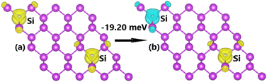
Fig. 11 illustrates the FM and AFM ordering in Si-doped bismuthene monolayer, where the latter is proven to be energetically more favorable exhibiting an energy of 19.20 meV smaller than the former. This result indicates that the Pauli repulsion between Si-pz electrons is even stronger in the C-doped system, which is predominant over Coulomb repulsion. The calculated BSs indicate the ferromagnetic and antiferromagnetic semiconductor natures considering the semiconductor character in both spin configurations (see Fig. 12). Specifically, band gap of 0.58 and 0.38 eV are obtained in the spin-up and spin-down channels for FM states, while both spin states possess energy gap of 0.50 eV for AFM state.
 |
| | Fig. 11 Spin ordering in the Si-doped bismuthene monolayer (spin-up: yellow surface; spin-down: cyan surface; iso-surface value: 0.002). | |
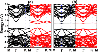 |
| | Fig. 12 Electronic band structure (spin-up: black curve; spin-down: red curve) of the Si-doped bismuthene monolayer with (a) ferromagnetic and (b) antiferromagnetic ordering. | |
D. Ge-doped bismuthene monolayer
As given in Table 1, the chemical bond length dGe–Bi is smaller than original dBi–Bi caused by a smaller atomic size of Ge atom as compared to Bi atom. Meanwhile, the structural wrinkle dGe–Bi exhibits a dependence on the supercell size. At high doping level, Ge dopant is relaxed moving inward, and the movement becomes quite smaller according to decrease the dopant concentration.
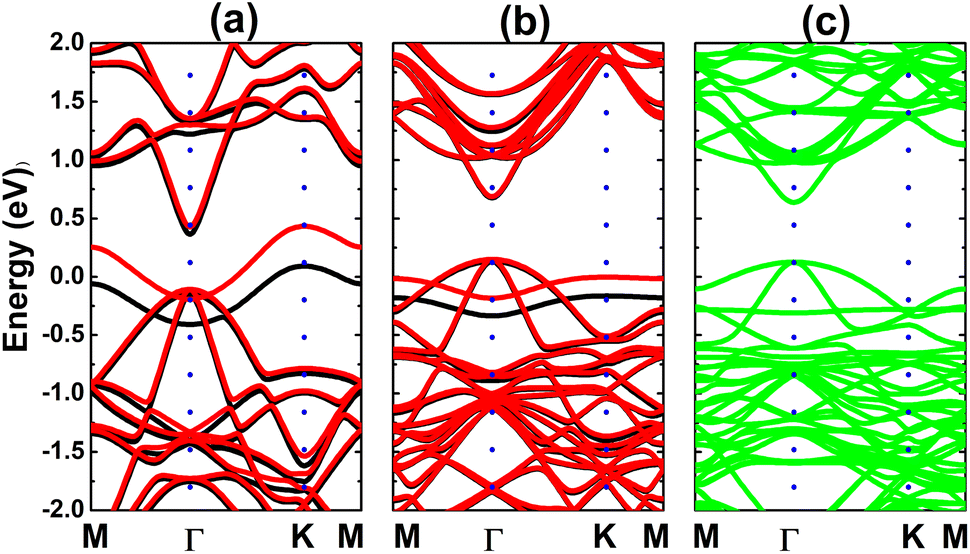
Calculated band structures of the Ge-doped bismuthene monolayer are displayed in Fig. 13. Our simulations assert the spin polarization at doping levels of 12.5% and 5.56%, meanwhile the spin channels are totally symmetric at lower dopant composition of 3.125%. In all cases, significant overlapping of energy branches and the Fermi level indicates metallic character of the doped systems. It can be noted doping-induced new energy flat curves, which are generated mainly by the Ge-pz state, which hybridizes significantly with Bi-pz state (see Fig. 14). As expected, Ge atom only exhibits important presence at the vicinity of the Fermi level, while Bi atoms are the main contributor to the valence band and conduction band. The Bader charge analysis indicates the charge transfer of −0.09 ÷ −0.10 e from host monolayer to the dopant. Therefore, one can conclude that Ge–Bi chemical bond is a mix of covalent character (generated by the electronic hybridization) and ionic character (generated by the charge transfer process).
 |
| | Fig. 13 Electronic band structure (spin-up: black curve; spin-down: red curve; non spin-polarized: green curve; the Fermi level is set to 0 eV) of the Ge-doped bismuthene monolayer with doping level of (a) 12.5%, (b) 5.56%, and (c) 3.125%. | |
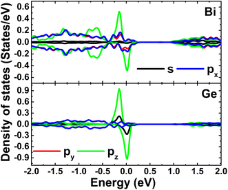 |
| | Fig. 14 Projected density of Ge dopant and its first Bi neighbor (the Fermi level is set to 0 eV) of the Ge-doped bismuthene monolayer with doping level of 5.56%. | |
It is found that bismuthene monolayer is magnetized by Ge doping at 12.5% and 5.56% with total magnetic moments of 0.60 and 0.44 μB, respectively. In these cases, the magnetism is generated mainly by Ge dopant and first Bi atoms from the doping site. This feature is also supported by the spin density illustrated in Fig. 6g and h. At lower doping level, magnetic properties disappear as a result of a stronger electronic hybridization between the magnetizing agent electronic states, that is Ge-pz and Bi-pz states.
IV. Conclusions
In summary, first-principles calculations have been performed to investigate systematically the effects of IVA-group atoms doping on the structural, electronic, and magnetic properties of bismuthene monolayer. Pristine monolayer is a direct gap semiconductor, whose band structure is build mainly by the sp3 hybridization. The incorporation of C, Si, and Ge incorporation causes structural local distortion due to the difference in atomic size of dopants and host Bi atoms. The effects decreases according to increasing the atomic number of IVA-group atoms. Consequently, doping process may require less energy as suggested by the decrease of doping energy in this direction. C–Bi chemical bond is predominantly ionic generated by the charge transfer from host monolayer to C atom, while Si–Bi and Ge–Bi bonds exhibit both covalent and ionic characters. Unless the case of doping with 3.125% of Ge atom, significant magnetization takes place, where magnetic properties are generated mainly by the outermost pz state of dopants and their Bi neighbor. Calculations indicate that AFM state is energetically more favorable, exhibiting energy of 2.90 and 19.20 meV lower than FM state in the C- and Si-doped monoalyers, respectively. The half-metallicity with semiconductor spin-up channel and metallic spin-down channel is obtained by doping with 12.5% of C atom, while a 3.125% composition leads to the formation of magnetic semiconductor 2D material similar to the Si-doped systems. In contrast, the metallization occurs in the remaining cases. This work may pave a solid way to functionalize bismuthene monolayer, recommending new 2D d0 materials with suitable properties for spintronic applications.
Conflicts of interest
The authors declare that they have no known competing financial interests or personal relationships that could have appeared to influence the work reported in this paper.
Acknowledgements
This research is funded by Thu Dau Mot University under grant number DT.22.1-018. Also, this research used resources of the high-performance computing cluster (HPCC) of Thu Dau Mot University (TDMU), Binh Duong Province, Vietnam.
References
- K. S. Novoselov, A. K. Geim, S. V. Morozov, D.-e. Jiang, Y. Zhang, S. V. Dubonos, I. V. Grigorieva and A. A. Firsov, Electric field effect in atomically thin carbon films, science, 2004, 306(5696), 666–669 CrossRef CAS PubMed.
- X. J. Lee, B. Y. Z. Hiew, K. C. Lai, L. Y. Lee, S. Gan, S. Thangalazhy-Gopakumar and S. Rigby, Review on graphene and its derivatives: Synthesis methods and potential industrial implementation, J. Taiwan Inst. Chem. Eng., 2019, 98, 163–180 CrossRef CAS.
- M. Tahriri, M. Del Monico, A. Moghanian, M. T. Yaraki, R. Torres, A. Yadegari and L. Tayebi, Graphene and its derivatives: Opportunities and challenges in dentistry, Mater. Sci. Eng., C, 2019, 102, 171–185 CrossRef CAS PubMed.
- S. Z. Butler, S. M. Hollen, L. Cao, Y. Cui, J. A. Gupta, H. R. Gutiérrez, T. F. Heinz, S. S. Hong, J. Huang and A. F. Ismach, et al., Progress, challenges, and opportunities in two-dimensional materials beyond graphene, ACS Nano, 2013, 7(4), 2898–2926 CrossRef CAS PubMed.
- G. R. Bhimanapati, Z. Lin, V. Meunier, Y. Jung, J. Cha, S. Das, D. Xiao, Y. Son, M. S. Strano and V. R. Cooper, et al., Recent advances in two-dimensional materials beyond graphene, ACS Nano, 2015, 9(12), 11509–11539 CrossRef CAS PubMed.
- J. S. Ponraj, Z.-Q. Xu, S. C. Dhanabalan, H. Mu, Y. Wang, J. Yuan, P. Li, S. Thakur, M. Ashrafi and K. Mccoubrey, et al., Photonics and optoelectronics of two-dimensional materials beyond graphene, Nanotechnology, 2016, 27(46), 462001 CrossRef PubMed.
- F. Reis, G. Li, L. Dudy, M. Bauernfeind, S. Glass, W. Hanke, R. Thomale, J. Schäfer and R. Claessen, Bismuthene on a sic substrate: A candidate for a high-temperature quantum spin hall material, Science, 2017, 357(6348), 287–290 CrossRef CAS PubMed.
- F. Yang, A. O. Elnabawy, R. Schimmenti, P. Song, J. Wang, Z. Peng, S. Yao, R. Deng, S. Song and Y. Lin, et al., Bismuthene for highly efficient carbon dioxide electroreduction reaction, Nat. Commun., 2020, 11(1), 1–8 CrossRef CAS PubMed.
- W. Ma, J. Bu, Z. Liu, C. Yan, Y. Yao, N. Chang, H. Zhang, T. Wang and J. Zhang, Monoclinic scheelite bismuth vanadate derived bismuthene nanosheets with rapid kinetics for electrochemically reducing carbon dioxide to formate, Adv. Funct. Mater., 2021, 31(4), 2006704 CrossRef CAS.
- I. Torres, A. M. Villa-Manso, M. Revenga-Parra, C. Gutiérrez-Sánchez, D. A. Aldave, E. Salagre, E. G. Michel, M. Varela, J. Gómez-Herrero and E. Lorenzo, et al., Preparation of high-quality few-layers bismuthene hexagons, Appl. Mater. Today, 2022, 26, 101360 CrossRef.
- D. Kecik, V. Özçelik, E. Durgun and S. Ciraci, Structure dependent optoelectronic properties of monolayer antimonene, bismuthene and their binary compound, Phys. Chem. Chem. Phys., 2019, 21(15), 7907–7917 RSC.
- R. N. Somaiya, Y. Sonvane and S. K. Gupta, Dependence of strain on the electronic and thermoelectric properties, Advances in Spectroscopy: Molecules to Materials, Proceedings of NCASMM, 2019, 236, 397 CAS.
- Z. Sun, H. Chu, S. Zhao, G. Li and D. Li, Optical properties enhancement of buckled bismuthene in mid-infrared region: a theoretical first-principle study, Mol. Simul., 2020, 46(13), 1004–1010 CrossRef CAS.
- M. Qi, S. Dai and P. Wu, Prediction of electronic and magnetic properties in 3d-transition-metal X-doped bismuthene (X = V, Cr, Mn and Fe), Appl. Surf. Sci., 2019, 486, 58–64 CrossRef CAS.
- I. khan Muhammad, K. Swera and M. Abdul, Computational study of 4d transition metals doped bismuthene for spintronics, Phys. E, 2021, 126, 114464 CrossRef.
- C. Xu, M. Zhu, H. Zheng, X. Du, W. Wang and Y. Yan, Stability, electronic structure and magnetic properties of vacancy and nonmetallic atom-doped buckled arsenene: first-principles study, RSC Adv., 2016, 6(49), 43794–43801 RSC.
- H. Zheng, J. Zhang, B. Yang, X. Du and Y. Yan, A first-principles study on the magnetic properties of nonmetal atom doped phosphorene monolayers, Phys. Chem. Chem. Phys., 2015, 17(25), 16341–16350 RSC.
- W. Kohn and L. J. Sham, Self-consistent equations including exchange and correlation effects, Phys. Rev., 1965, 140(4A), A1133 CrossRef.
- G. Kresse and J. Furthmüller, Efficiency of ab-initio total energy calculations for metals and semiconductors using a plane-wave basis set, Comput. Mater. Sci., 1996, 6(1), 15–50 CrossRef CAS.
- G. Kresse and J. Furthmüller, Efficient iterative schemes for ab initio total-energy calculations using a plane-wave basis set, Phys. Rev. B: Condens. Matter Mater. Phys., 1996, 54(16), 11169 CrossRef CAS PubMed.
- J. P. Perdew, K. Burke and M. Ernzerhof, Generalized gradient approximation made simple, Phys. Rev. Lett., 1996, 77(18), 3865 CrossRef CAS PubMed.
- H. J. Monkhorst and J. D. Pack, Special points for Brillouin-zone integrations, Phys. Rev. B: Condens. Matter Mater. Phys., 1976, 13(12), 5188 CrossRef.
- M.-Y. Liu, Y. Huang, Q.-Y. Chen, Z.-Y. Li, C. Cao and Y. He, Strain and electric field tunable electronic structure of buckled bismuthene, RSC Adv., 2017, 7(63), 39546–39555 RSC.
- M. Pumera and Z. Sofer, 2D monoelemental arsenene, antimonene, and bismuthene: beyond black phosphorus, Adv. Mater., 2017, 29(21), 1605299 CrossRef PubMed.
- V. Alijani, J. Winterlik, G. H. Fecher, S. S. Naghavi and C. Felser, Quaternary half-metallic Heusler ferromagnets for spintronics applications, Phys. Rev. B, 2011, 83(18), 184428 CrossRef.
- G. Bhattacharyya, P. Garg, P. Bhauriyal and B. Pathak, Density functional theory study of defect induced ferromagnetism and half-metallicity in CaI2 based monolayer for spintronics applications, ACS Appl. Nano Mater., 2019, 2(10), 6152–6161 CrossRef CAS.
- T. R. Paudel and E. Y. Tsymbal, Spin filtering in CrI3 tunnel junctions, ACS Appl. Mater. Interfaces, 2019, 11(17), 15781–15787 CrossRef CAS PubMed.
|
| This journal is © The Royal Society of Chemistry 2023 |
Click here to see how this site uses Cookies. View our privacy policy here. 
 Open Access Article
 This Open Access Article is licensed under a Creative Commons Attribution-Non Commercial 3.0 Unported Licence
 *cd
*cd