
 Open Access Article
 This Open Access Article is licensed under a
 Creative Commons Attribution 3.0 Unported Licence
Exciton–phonon coupling in two-dimensional layered (BA)2PbI4 perovskite microplates†
Yixiong Wangb,
Chenglin Hea,
Qin Tana,
Zilan Tanga,
Lanyu Huangb,
Liang Liua,
Jiaocheng Yina,
Ying Jiangb,
Xiaoxia Wang*a and
Anlian Pan *a
*a
aKey Laboratory for Micro-Nano Physics and Technology of Hunan Province, State Key Laboratory of Chemo/Biosensing and Chemometrics, College of Materials Science and Engineering, Hunan University, Changsha, Hunan 410082, China. E-mail: wangxiaoxia@hnu.edu.cn; anlian.pan@hnu.edu.cn
bSchool of Physics and Electronics, Hunan University, Changsha, Hunan 410082, China
First published on 17th February 2023
Abstract
Two-dimensional layered (BA)2PbI4 (BA = C4H9NH3) perovskites are emerging as a new class of layered materials and show great potential in optoelectronic applications. Elucidating how exciton–phonon interaction affects the excitonic emission is of great importance for a better knowledge of their optoelectronic properties. In this letter, we synthesized high-quality (BA)2PbI4 microplates via solution methods, and dual-excitonic emission peaks (surface-emission and interior-emission) were detected from the as-grown samples at low temperatures. Furthermore, we determine the energies for the longitudinal optical phonon modes to be ∼27 and ∼18 meV, and the exciton–phonon coupling strengths to be ∼177 and ∼21 meV for the surface-emission and interior-emission bands, respectively. Compared to the interior-emission band, the stronger exciton–phonon interaction results in a considerable degree of spectral broadening and red-shift for the surface-emission with increasing temperature. In contrast, the (OA)2PbI4 (OA = C8H17NH2) microplates with longer alkyl chains between Pb–I layers, exhibit only one excitonic emission peak, as well as a large exciton–phonon coupling strength. Our work clarifies the influence of exciton–phonon coupling on the excitonic emission of (BA)2PbI4 microplates, and also suggests the intrinsic relationship between the exciton–phonon coupling and the length of organic carbon chain ligands.
Introduction
Two-dimensional (2D) perovskite materials are layered analogs of three-dimensional organic and inorganic hybrid halide perovskites, formed by larger alkyl ammonium cations partially or completely replacing commonly used methylammonium (MA) cations.1–3 Benefiting from advantages such as a simple preparation method,4–6 quantum well structure,7,8 and high exciton binding energy,9–11 these layered perovskites have been extensively studied and applied in light-emitting diodes,12–14 photodetectors,15–17 and solar cells.18,19 Among them, (BA)2PbI4 perovskites with butylammonium (BA+) organic cations shows novel photoluminescence (PL) characteristics due to its dynamic disorder and phase change originating from a relatively soft lattice structure.20 Meanwhile, crystallization conditions and the introduction of intrinsic defects and impurities will directly affect the photoelectric properties. In addition, (BA)2PbI4 with n = 1 is a simple and stable phase with strong excitonic emission in the visible region, which enables (BA)2PbI4 single crystals as a promising candidate to study the photophysical properties of 2D perovskites.21Particularly, the dual-excitonic emission peak in (BA)2PbI4 crystalline has arisen in an intensive study. For instance, DeCrescent et al. demonstrate that the low-energy emission is due to magnetic dipole emission induced by p-like excitons, which self-trapped at a lower energy of 1s excitons than the primary electric dipole.22 Du et al. latest research suggest that this dual emission peak is induced by cation accumulation in (BA)2PbI4 bulk materials. Lattice residual strain originates from the decreased mobility of organic cations in the bulk or interior of the crystal.23 Recently, a demonstration of electronic interactions between the inorganic Pb–I layers was verified by intercalation of long-chain organic molecules in the layered perovskite single crystals at room temperature.24 These findings further validated prior's prediction that (BA)2PbI4 had a dual bandgap formed in the inside and the surface of the crystal. Generally, in the polar lattice of lead halide perovskites, it has become widely accepted that the Fröhlich interaction between exciton and optical phonons is crucial in describing its photonics properties. Subsequently, the dual emission peak of (BA)2PbI4 was also explained at a molecular level, revealing that a phonon replica of the excitonic state leads to the lower energy emission.25 It is not difficult to find that prior studies (BA)2PbI4 perovskites are most focused on the origin of the dual-emission peak, the specific influence of exciton–phonon interaction on the excitonic emission of (BA)2PbI4 perovskites remains elusive.
Here, single-crystal (BA)2PbI4 microplates were synthesized using a solution method. A typical excitonic recombination emission characteristic can be observed from the as-grown (BA)2PbI4 microplates at both the room temperature and low temperature. Furthermore, we examined the temperature dependence of the full width at half maximum (FWHM) and peak positions of the PL spectra. It is found that the exciton–phonon coupling of the surface emission is substantially stronger in comparison with that of the interior-emission, resulting in a considerable degree of the line width broadening for the surface-emission and a red-shift of bandgap with temperature increasing. In contrast, due to the longer alkyl chains between Pb–I layers in (OA)2PbI4 crystals, only one excitonic emission peak with strong exciton–phonon coupling is detected from (OA)2PbI4 microplates.
Results
The crystal structure of (BA)2PbI4 is shown in Fig. 1(a). The corner-shared [PbI6]4− octahedra constitutes a layered semiconducting phase in this structure, which is separated by an insulating organic spacer BA+, generating a repeating quantum well structure. Fig. 1(b) shows the schematic diagram for the growth of (BA)2PbI4 microplates by using a solution strategy. The obtained (BA)2PbI4 microplates have a uniform morphology with tens of micrometers in lateral dimension and hundreds of micrometers in length, as illustrated in Fig. 1(c and d). Fig. 1(f) shows the enlarged SEM image of the marked region with a red rectangle in Fig. 1(d). It is found that the sample exhibits an excellent surface smoothness and a neat edge with a thickness of ∼337 nm [Fig. 1(e)], which indicates a high quality of the as-grown (BA)2PbI4 microplates. Additionally, the thickness of (BA)2PbI4 microplates can be precisely controlled by changing the temperature of the precursor (Fig. S1†). Fig. 1(g) shows the XRD of the (BA)2PbI4 microplates alongside a reference generated from single-crystal data, which shows a typical (00l) plane pattern of layered perovskites. Note that the position of the dominant diffraction peaks is almost similar when compared our experimental results with the reference data. Generally, the overall peak intensity depends more on the crystallinity of the sample and the signal of the experimental instrument.26 Herein, by comparing the peak position of the experimental and the reference of the XRD pattern, it is concluded that the crystal structure of the perovskites in this manuscript is consistent with the crystal structure in the reference. The high agreement between the experimental and calculated diffraction patterns indicates that the material is phase pure.20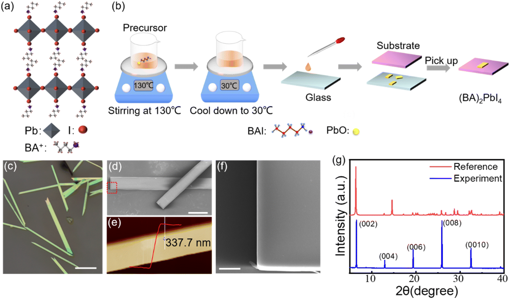 | ||
| Fig. 1 (a) Schematic diagram of the crystalline structure of (BA)2PbI4. (b) Schematic illustration of growth process of the (BA)2PbI4 microplates. (c) Optical image of the as-grown (BA)2PbI4 microplates. Scale bar is 200 μm. (d) SEM image of (BA)2PbI4. Scale bar is 40 μm. (e) AFM image of a representative (BA)2PbI4 microplate. (f) The enlarged SEM image of the marked region with a red rectangle in (d). Scale bar is 5 μm. (g) XRD spectra of the (BA)2PbI4 microplates along with the reference calculated from single crystal data. | ||
An initial characterization of these single (BA)2PbI4 microplates is conducted via photoluminescence (PL) measurements, as shown in Fig. 2(a). The line-scan PL of a single microplate at room temperature show a uniform emission intensity at 2.37 eV and similar spectra profile, which further revealed a uniform crystalline quality of the as-grown sample. The UV-vis absorption spectra of the (BA)2PbI4 microplate at room temperature shows a strong absorbance that is associated with PL emission peak (Fig. S2†), which indicates that the PL peaks are not generated by defect states.27 While, at 77 K, the (BA)2PbI4 microplate exhibits prominent dual emission peaks located at 2.54 eV (488 nm) and 2.40 eV (517 nm) with a line-width of 22.56 meV and 11.04 meV, much narrower than that at room temperature. Note that the sample exhibits a broad emission ranging from ∼1.6 eV to ∼2.3 eV at lower temperatures. Such broad emission has been previously reported as self-trapped emission.28–30 The linear fitting of the emission peak intensity with the excitation power yields a slope of ∼1 both at room temperature and low temperature (Fig. S3†), which is consistent with an excitonic recombination process due to the large exciton binding energy of this type of 2D perovskites.9,10,31 In general, two-photon excitation show a deeper penetration depth into the microplate than one-photon excitation (400 nm), resulting in a high contribution of PL emission from the interior part of the sample. Fig. S4† shows the intensity of the emission peak located at 2.40 eV excited by 800 nm is much stronger than that observed with a 400 nm light excitation. To exclude that the photon might be in resonances with an intersubband transition when excited with 800 nm, the two-photon excitation process with another wavelength at 900 nm were studied (Fig. S5†). By examining the PL spectrum of (BA)2PbI4 with various thicknesses (Fig. S6†), we find the intensity of the low-energy emission peak increased as the thickness grew, further indicating the low-energy peak is associated with interior part emission of the sample and in consistent with the demonstration by Nag et al.32 Furthermore, the PL spectra of (BA)2PbI4 microplate at different focal points at 77 K were measured. As shown in the Fig. S7,† with the focal point changed (excitation depth changed), the intensity of the 2.40 eV emission has changed, which further demonstrates that the 2.40 eV emission originates from the “interior” part of the sample. Such that, we define the high energy emission at 2.54 eV and the low energy emission at 2.40 eV by using surface-emission (SE) and interior-emission (IE), respectively.
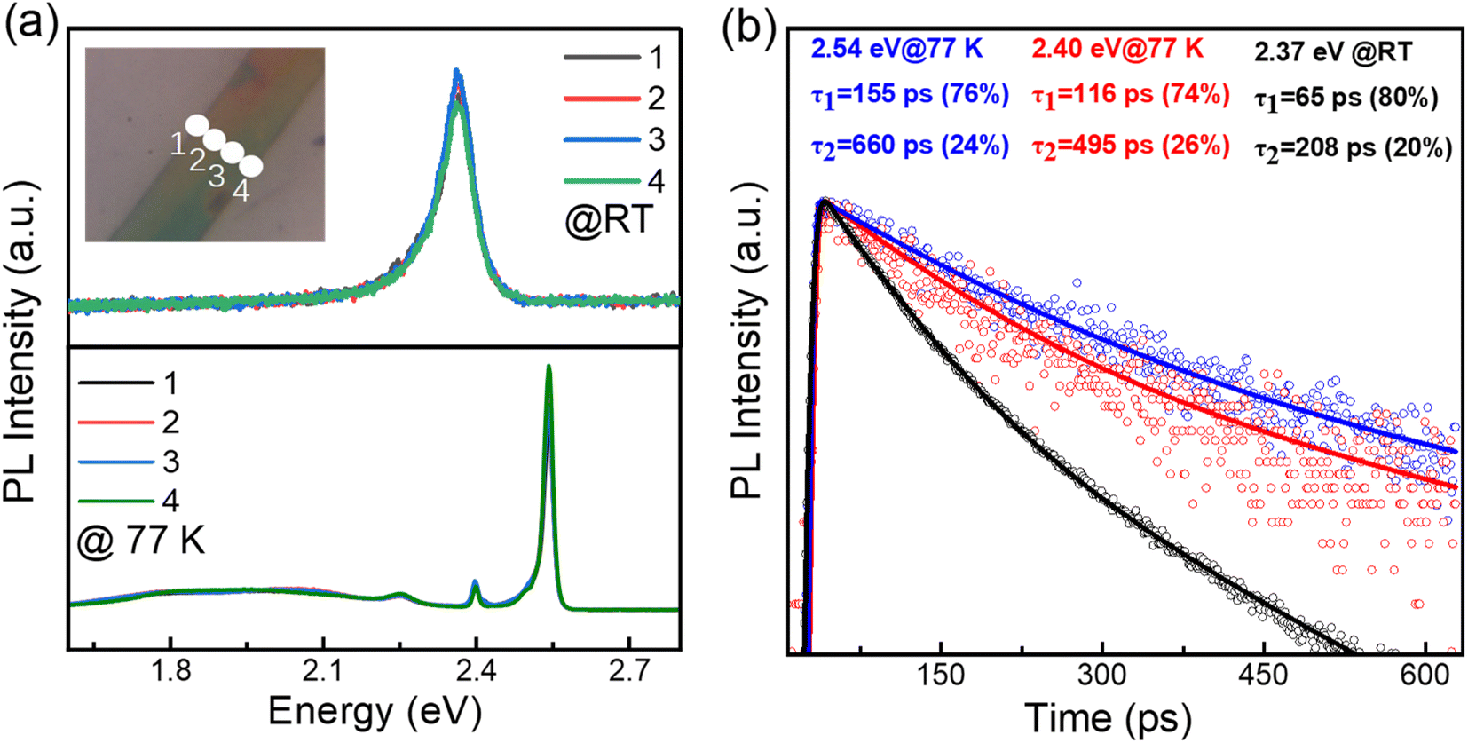 | ||
| Fig. 2 (a and b) Spatially-resolved PL emission spectra detected at room temperature (up panel) and at 77 K (bottom panel), locations are marked at inset of (a). (b) PL decay dynamics of the emission peaks of 2.54 eV and 2.40 eV at 77 K and 2.37 eV at room temperature, respectively. | ||
The time-resolved PL dynamics are further measured by streak camera and the results are shown in Fig. 2(b). At 77 K, the PL emissions show a biexponential decay feature with lifetimes of 155 ps (76%) and 662 ps (24%) for 2.54 eV emission, 116 ps (74%) and 495 ps (26%) for 2.40 eV emission, respectively. While, the room temperature PL lifetime of 65 ps (80%) and 208 ps (20%) is faster than that at low temperature, which could be ascribed to the inevitable increased nonradiative recombination channels at high temperature. These relatively short PL lifetimes further excluded the possibility of defect or trap-state emission, which usually have a lifetime as long as 100 ns.33
Temperature-dependent photoluminescence spectra have long been used to investigate exciton–phonon coupling mechanisms in a variety of semiconductor materials.34 Fig. 3(a) shows the 2D pseudo-color plot of temperature-dependent normalized photoluminescence spectra of the (BA)2PbI4 microplate. It is found that the IE band mainly emerged at low temperature range and vanished gradually when beyond ∼160 K, while the SE band keep existing with the temperature increasing and shift to ∼2.37 eV at 270 K is due to an phase transition,35 as also clearly shown in the temperature-dependent spectra [Fig. 3(b)]. The SE band is the low-temperature phase of (BA)2PbI4. It is noted that the SE band emission at ∼2.54 eV is the low-temperature phase of (BA)2PbI4. The phase transition occurs around ∼270 K and is related to the reconfiguration of BA molecule, which also affects the inorganic framework.36 During the phase transition process, the high-temperature domains within the crystal structure are created, which is frozen-out and manifested as an additional low-energy contribution around 2.4 eV,37,38 shown in Fig. 3(a). In addition, it is found that the 2.4 eV emission mainly emerged at low temperature range and vanished gradually when beyond ∼160 K [Fig. 3(b)], which is also consistent with the statement of the frozen-out of the high-temperature domains. There is no obvious defect-state associated broadband emission at the lower energy side throughout the temperature range, indicates a high crystalline quality of the (BA)2PbI4 microplate as compared to previously reported (BA)2PbI4 film or bulk crystals.27,32 In addition, the linewidth of both the SE and IE significantly narrower at low temperature, as to be expected due to a reduced contribution of exciton–phonon coupling stemming from diminishing phonon populations.39 Remarkably, the degree of this narrowing is different (∼10 meV for the IE and 43 meV for the SE) after we extracted the temperature dependence of the FWHM of the two emission peaks, as shown in Fig. 3(c).
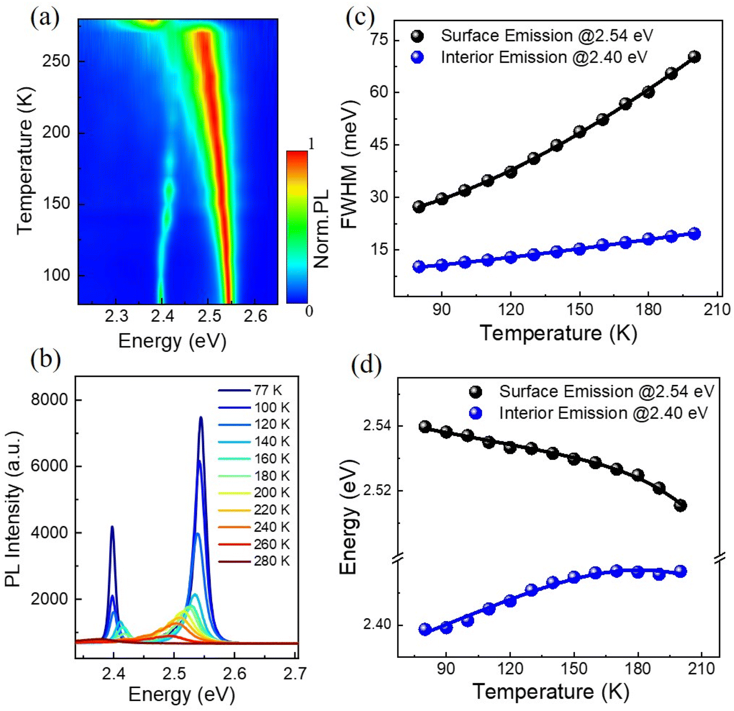 | ||
| Fig. 3 (a) The PL spectra of a 2D pseudo-color plot of the (BA)2PbI4 microplate at temperatures from 77 to 280 K. (b) Temperature-dependent PL spectrum of (BA)2PbI4 microplate. (c) The FWHM of the PL peak as a function of temperature extracted out from (b); dots: experimental data and line: the fitting curve. (d) The emission peak energy as a function of temperature extracted out from (b); dots: experimental data and line: the fitting curve. | ||
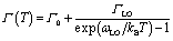
In general, the primary contribution to the temperature-dependent linewidth broadening is determined to be the Fröhlich interaction of excitons with longitudinal-optical phonons (LO), while acoustic phonons or impurity scattering usually playing a diminished role. To further quantify the Fröhlich coupling strength of this dual-excitonic emission, we employ the following model to fitting their temperature dependence line width broadening:34
 | (1) |
The temperature dependence of the peak position is analyzed as a further step in getting more knowledge about the exciton–phonon interaction of the dual-emission band. It is noted that the surface emission redshifts as the temperature rises, but the interior emission follows an opposite trend [Fig. 3(b)], which differs from previously reported dual-peak emission of bulk (BA)2PbI4 perovskites.32 For perovskite materials systems, when the temperature rises, thermal-induced lattice expansion reduces the valence bandwidth and thus increases the bandgap (Eg).43 Simultaneously, the electron–phonon interaction will be enhanced since the phonon density growing with temperature, enabling a red-shift of emission energy. As a result, the variation of Eg with temperature should be a competitive effect between lattice thermal expansion (TE) and exciton–phonon (EP) coupling. By assuming a linear relationship between lattice constant and temperature bandgap, the temperature-dependence bandgap variation of the dual-excitonic emission can be fitted by the following expression:44
 | (2) |
As prior report demonstrate that lower-energy emission is induced by the organic cation stacking effect in the interior part.24 Such that the above results and discussions might suggests that longer alkyl chains of surface regime induce a larger local lattice distortion in the Pb–I layers compared to the shorter chains of the interior part, resulting a stronger exciton–phonon interaction in the surface emission (BA)2PbI4 perovskites. Additionally, as the temperature increase, lattice expansion will counteract this stacking effect, thus the interior emission band disappeared.
In order to probe the correlation between the exciton–phonon coupling and the alkyl chains length of the organic cations, we further fabricate (OA)2PbI4 microplates and studied the temperature dependent PL. The XRD patterns in Fig. 4(a) show the peaks are shifted toward the lower 2θ values from (BA)2PbI4 to (OA)2PbI4. In order to accurately analyze the Pb–I inorganic layer spacing of (BA)2PbI4 and (OA)2PbI4, the small angle XRD patterns were further obtained (Fig. S8†). According to their small angle XRD data, the Pb–I inorganic layer spacing is calculated to be 13.59 Å for (BA)2PbI4 and 18.41 Å for (OA)2PbI4 by Bragg's law, respectively.45 As the lattice structure depicted in Fig. 4(b), the difference between (OA)2PbI4 and (BA)2PbI4 mainly lies in alkyl chain length. While BA+ and OA+ are both linear alkyl chains within the same group, which has little effect on their emission wavelength with the main peak located at 2.54 eV at 77 K, as can be seen in Fig. 4(c). However, unlike the dual-excitonic peak detected from (BA)2PbI4, (OA)2PbI4 only show one emission peak within the temperature window we examined and just as the spectra profile of surface emission for (BA)2PbI4. In addition, by fitting the temperature-dependence FWHM of the PL spectra, we obtained the LO phonon energy and the exciton–phonon coupling strength of ωLO ∼ 34 meV and ΓLO ∼ 122 meV, respectively [Fig. 4(d)]. The obtained LO phonon energy is a little bit large than the surface emission of (BA)2PbI4, which further indicates longer alkyl chains is responsible for a large local lattice distortion and higher phonon energy. In addition, the strong exciton–phonon interaction similar as detected from the surface emission of (BA)2PbI4. These observations demonstrate the intrinsic correlation between the exciton–phonon coupling and the length of alkyl chain of two-dimensional layered hybrid perovskites, as well as the origin of lower energy emission.
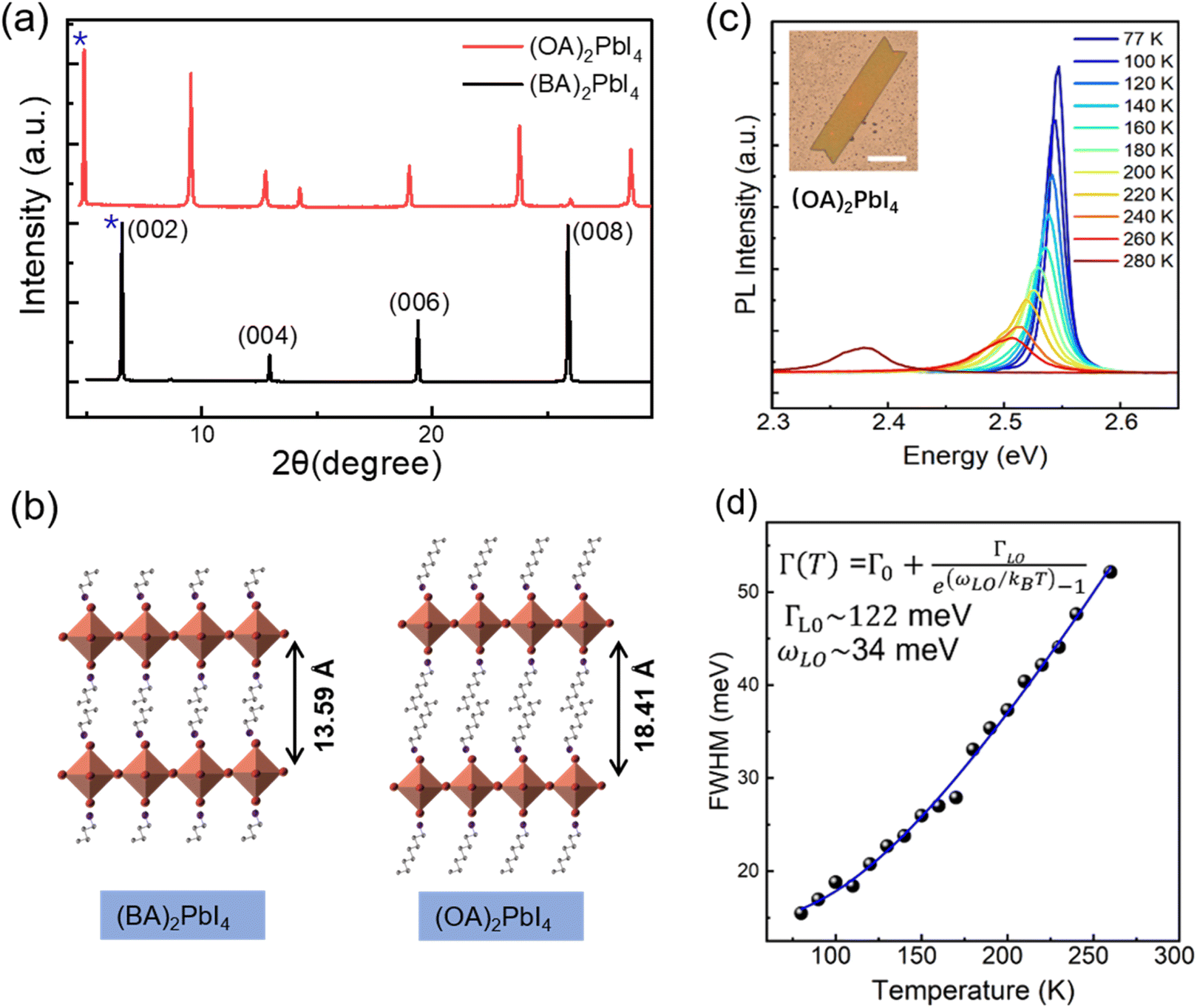 | ||
| Fig. 4 (a) XRD spectra of the (BA)2PbI4 and (OA)2PbI4 microplates. (b) Schematic of crystal structures of (BA)2PbI4 and (OA)2PbI4 showing interlayer distance obtained from XRD patterns shown in (a). (c) Temperature-dependent PL spectra of (OA)2PbI4 microplate, inset is the optical image of single (OA)2PbI4 microplate, the scale bar is 50 μm. (d) The FWHM of the PL peak as a function of temperature extracted out from (c); dots: experimental data and line: the fitting curve. | ||
Conclusions
In conclusion, we have experimentally studied the influence of exciton–phonon coupling on the excitonic emission in (BA)2PbI4. The excitation power-dependent PL both in room temperature and 77 K indicate a typical excitonic recombination characteristic of the as-grown (BA)2PbI4 microplates. According to the temperature dependent PL, the exciton–phonon interaction strength of the surface-emission is much stronger than that of the interior-emission, resulting a redshift of the emission spectrum and larger bandwidth broadening. In contrast, only single emission peak was detected from (OA)2PbI4 microplates and distance between Pb–I inorganic layers of (OA)2PbI4 is larger than that of (BA)2PbI4, indicating the length of alkyl chains affects the lattice distortions of Pb–I layers and the exciton–phonon coupling in 2D layered perovskites. Our findings will be beneficial for the optimization of light sources based on 2D layered halide perovskites.Conflicts of interest
There are no conflicts to declare.Acknowledgements
This work was financially supported by the National Natural Science Foundation of China (52221001, U19A2090, 62090035, and 62175061), the Key Program of the Hunan Provincial Science and Technology Department (No. 2019XK2001, 2020XK2001), the International Science and Technology Innovation Cooperation Base of Hunan Province (No. 2018WK4004), and the Natural Science Foundation of Hunan Province (2022JJ30167).References
- E. Shi, B. Yuan, S. B. Shiring, Y. Gao, Akriti, Y. Guo, C. Su, M. Lai, P. Yang, J. Kong, B. M. Savoie, Y. Yu and L. Dou, Nature, 2020, 580, 614–620 CrossRef CAS PubMed
.
- C. Liang, H. Gu, Y. Xia, Z. Wang, X. Liu, J. Xia, S. Zuo, Y. Hu, X. Gao, W. Hui, L. Chao, T. Niu, M. Fang, H. Lu, H. Dong, H. Yu, S. Chen, X. Ran, L. Song, B. Li, J. Zhang, Y. Peng, G. Shao, J. Wang, Y. Chen, G. Xing and W. Huang, Nat. Energy, 2020, 6, 38–45 CrossRef
- J. A. Sichert, A. Hemmerling, C. Cardenas-Daw, A. S. Urban and J. Feldmann, APL Mater., 2019, 7, 041116 CrossRef
- Y. Liu, Y. Zhang, Z. Yang, H. Ye, J. Feng, Z. Xu, X. Zhang, R. Munir, J. Liu, P. Zuo, Q. Li, M. Hu, L. Meng, K. Wang, D. M. Smilgies, G. Zhao, H. Xu, Z. Yang, A. Amassian, J. Li, K. Zhao and S. F. Liu, Nat. Commun., 2018, 9, 5302 CrossRef CAS PubMed
- I. W. H. Oswald, A. A. Koegel and J. R. Neilson, Chem. Mater., 2018, 30, 8606–8614 CrossRef CAS
- L. Zhu, H. Zhang, Q. Lu, Y. Wang, Z. Deng, Y. Hu, Z. Lou, Q. Cui, Y. Hou and F. Teng, J. Mater. Chem. C, 2018, 6, 3945–3950 RSC
- X. Hong, T. Ishihara and A. V. Nurmikko, Phys. Rev. B: Condens. Matter Mater. Phys., 1992, 45, 6961–6964 CrossRef CAS PubMed
- G. Walters, M. Wei, O. Voznyy, R. Quintero-Bermudez, A. Kiani, D. M. Smilgies, R. Munir, A. Amassian, S. Hoogland and E. Sargent, Nat. Commun., 2018, 9, 4214 CrossRef CAS PubMed
- K. Tanaka, T. Takahashi, T. Kondo, T. Umebayashi, K. Asai and K. Ema, Phys. Rev. B: Condens. Matter Mater. Phys., 2005, 71, 045312 CrossRef
- M. C. Gelvez-Rueda, E. M. Hutter, D. H. Cao, N. Renaud, C. C. Stoumpos, J. T. Hupp, T. J. Savenije, M. G. Kanatzidis and F. C. Grozema, J. Phys. Chem. C, 2017, 121, 26566–26574 CrossRef CAS PubMed
- W. Li, J. Ma, H. Wang, C. Fang, H. Luo and D. Li, Nanophotonics, 2020, 9, 2001–2006 CrossRef CAS
- H. Chen, J. Lin, J. Kang, Q. Kong, D. Lu, J. Kang, M. Lai, L. N. Quan, Z. Lin, J. Jin, L. W. Wang, M. F. Toney and P. Yang, Sci. Adv., 2020, 6, eaay4045 CrossRef CAS PubMed
- P. Vashishtha, M. Ng, S. B. Shivarudraiah and J. E. Halpert, Chem. Mater., 2018, 31, 83–89 CrossRef
- J. Byun, H. Cho, C. Wolf, M. Jang, A. Sadhanala, R. H. Friend, H. Yang and T. W. Lee, Adv. Mater., 2016, 28, 7515–7520 CrossRef CAS PubMed
- J. Zhou and J. Huang, Adv. Sci., 2018, 5, 1700256 CrossRef PubMed
- S. Yakunin, M. Sytnyk, D. Kriegner, S. Shrestha, M. Richter, G. J. Matt, H. Azimi, C. J. Brabec, J. Stangl, M. V. Kovalenko and W. Heiss, Nat. Photonics, 2015, 9, 444 CrossRef CAS PubMed
- Y. Fu, H. Zhu, A. W. Schrader, D. Liang, Q. Ding, P. Joshi, L. Hwang, X. Zhu and S. Jin, Nano Lett., 2016, 16, 1000 CrossRef CAS PubMed
- Q. Chen, H. P. Zhou, Z. R. Hong, S. Luo, H. S. Duan, H. H. Wang, Y. S. Liu, G. Li and Y. Yang, J. Am. Chem. Soc., 2014, 136, 622–625 CrossRef CAS PubMed
- H. Zhou, Q. Chen, G. Li, S. Luo, T. B. Song, H. S. Duan, Z. Hong, J. You, Y. Liu and Y. Yang, Science, 2014, 345, 542–546 CrossRef CAS PubMed
- D. G. Billing and A. Lemmerer, Acta Crystallogr., Sect. B: Struct. Sci., 2007, 63, 735–747 CrossRef CAS PubMed
- M. C. Gélvez-Rueda, S. Peeters, P. C. Wang, K. M. Felter and F. C. Grozema, Helv. Chim. Acta, 2020, 103, e2000121 CrossRef
- R. A. DeCrescent, X. Du, R. M. Kennard, N. R. Venkatesan, C. J. Dahlman, M. L. Chabinyc and J. A. Schuller, ACS Nano, 2020, 14, 8958–8968 CrossRef CAS PubMed
- Q. Du, C. Zhu, Z. Yin, G. Na, C. Cheng, Y. Han, N. Liu, X. Niu, H. Zhou, H. Chen, L. Zhang, S. Jin and Q. Chen, ACS Nano, 2020, 14, 5806–5817 CrossRef CAS PubMed
- T. Sheikh, V. Nawale, N. Pathoor, C. Phadnis, A. Chowdhury and A. Nag, Angew. Chem., Int. Ed., 2020, 59, 11653–11659 CrossRef CAS PubMed
- R. F. Moral, J. C. Germino, L. G. Bonato, D. B. Almeida, E. M. Therézio, T. D. Z. Atvars, S. D. Stranks, R. A. Nome and A. F. Nogueira, Adv. Opt. Mater., 2020, 8, 2001431 CrossRef CAS
- A. Goyal, I. Khatri, A. K. Singh, R. Sharma and M. Mohan, Radiat. Phys. Chem., 2017, 138, 16–21 CrossRef CAS
- J. Li, H. Wang and D. Li, Front. Optoelectron., 2020, 13, 225–234 CrossRef PubMed
- M. D. Smith and H. I. Karunadasa, Acc. Chem. Res., 2018, 51, 619–627 CrossRef CAS PubMed
- J. Xu, S. Li, C. Qin, Z. Feng and Y. Du, J. Phys. Chem. C, 2020, 124, 11625–11630 CrossRef CAS
- S. Li, J. Xu, Z. Li, Z. Zeng, W. Li, M. Cui, C. Qin and Y. Du, Chem. Mater., 2020, 32, 6525–6531 CrossRef CAS
- T. Schmidt, K. Lischka and W. Zulehner, Phys. Rev. B: Condens. Matter Mater. Phys., 1992, 45, 8989–8994 CrossRef PubMed
- T. Sheikh, A. Shinde, S. Mahamuni and A. Nag, ACS Energy Lett., 2018, 3, 2940–2946 CrossRef CAS
- M. J. Rao, T. Shibata, S. Chattopadhyay and A. Nag, J. Phys. Chem. Lett., 2013, 5, 167–173 CrossRef PubMed
- A. D. Wright, C. Verdi, R. L. Milot, G. E. Eperon, M. A. Perez-Osorio, H. J. Snaith, F. Giustino, M. B. Johnston and L. M. Herz, Nat. Commun., 2016, 7, 11755 CrossRef PubMed
- J. Wang, H. Shen, J. Li, W. Li, C. Fang, J. Ma, X. Cheng and D. Li, Appl. Phys. Lett., 2020, 116, 051103–511035 CrossRef PubMed
- O. Yaffey, A. Chernikovy, Z. M. Norman, Y. Zhong, A. Velauthapillai, A. v. d. Zande, J. S. Owen and T. F. Heinz, Phys. Rev. B: Condens. Matter Mater. Phys., 2015, 92, 045414 CrossRef
- M. Baranowski, S. J. Zelewski, M. Kepenekian, B. Traoré, J. M. Urban, A. Surrente, K. Galkowski, D. K. Maude, A. Kuc, E. P. Booker, R. Kudrawiec, S. D. Stranks and P. Plochocka, ACS Energy Lett., 2019, 4, 2386–2392 CrossRef CAS
- K. Galkowski, A. A. Mitioglu, A. Surrente, Z. Yang, D. K. Maude, P. Kossacki, G. E. Eperon, J. T. Wang, H. J. Snaith, P. Plochocka and R. J. Nicholas, Nanoscale, 2017, 9, 3222–3230 RSC
- O. H. Cheng, T. Qiao, M. Sheldon and D. H. Son, Nanoscale, 2020, 12, 13113–13118 RSC
- H. H. Fang, F. Wang, S. Adjokatse, N. Zhao, J. Even and M. Antonietta Loi, Light: Sci. Appl., 2016, 5, e16056 CrossRef CAS PubMed
- M. Gramlich, C. Lampe, J. Drewniok and A. S. Urban, J. Phys. Chem. Lett., 2021, 12, 11371–11377 CrossRef CAS PubMed
- L. Ni, U. Huynh, A. Cheminal, T. H. Thomas, R. Shivanna, T. F. Hinrichsen, S. Ahmad, A. Sadhanala and A. Rao, ACS Nano, 2017, 11, 10834–10843 CrossRef CAS PubMed
- S. Wang, J. Ma, W. Li, J. Wang, H. Wang, H. Shen, J. Li, J. Wang, H. Luo and D. Li, J. Phys. Chem. Lett., 2019, 10, 2546–2553 CrossRef CAS PubMed
- L. Yang, K. Wei, Z. Xu, F. Li, R. Chen, X. Zheng, X. Cheng and T. Jiang, Opt. Lett., 2018, 43, 122–125 CrossRef CAS PubMed
- H. Zhang, Z. Zeng, X. Shi and Y. Du, Nanoscale, 2021, 13, 13976–13994 RSC
Footnote |
| † Electronic supplementary information (ESI) available. See DOI: https://doi.org/10.1039/d2ra06401d |
| This journal is © The Royal Society of Chemistry 2023 |