
 Open Access Article
 This Open Access Article is licensed under a Creative Commons Attribution-Non Commercial 3.0 Unported Licence
Simultaneous passivation on both A and X sites of halogen perovskite with magnesium benzoate†
Chenxin Xua,
Lujie Liua,
Yurong Huangb,
Fei Zhangb and
Hui Cao *a
*a
aSchool of Chemistry and Materials Science, Nanjing University of Information Science and Technology, Nanjing 210044, People's Republic of China. E-mail: yccaoh@hotmail.com
bSchool of Environmental Science and Engineering, Nanjing University of Information Science and Technology, Nanjing 210044, People's Republic of China
First published on 16th January 2023
Abstract
Surface modification engineering is a well-known effective passivation method for making efficient and stable perovskite solar cells (PSCs). However, to our knowledge, little attention has been paid to simultaneously passivating the A and X sites of halogen perovskites. Herein, we introduced an organometallic salt (C6H5COO)2Mg (MgBEN) as a passivator, and as a result, the C6H5COOMg+ passivates the A site and C6H5COO− the X site on the perovskite layer, significantly reducing the trap-state density and nonradiative recombination. Moreover, the modification induces the perovskite film quality to improve, which may decrease the charge accumulation and facilitate carrier transport. By optimizing the concentration of the MgBEN, the perovskite film showed an increased grain size (from 1.18 μm to 1.61 μm), and the best device exhibited an enhanced power conversion efficiency (PCE) of 22.24%. Meanwhile, the device after modification performed with good long-term stability.
Introduction
Within the past decade, hybrid organic–inorganic metal halide perovskite materials have demonstrated various applications in optoelectronic devices, including photovoltaic,1,2 photodetectors,3,4 and light-emitting diodes.5 Among these, perovskite solar cells show great potential for next-generation photovoltaic technology due to their high light absorption coefficient,6 excellent carrier diffusion length,7 tuneable direct bandgap,8 and cost-efficient fabrication process.9 Recently, the state-of-the-art conventional n-i-p PSCs have realized 25.7%10 PCE compared with the original 3.8%.2 However, there is still considerable room to further boost the PCE of PSCs to reach the Shockley–Queisser limit,11 and the long-term stability of PSCs under actual operational conditions is still the major obstacle for their commercialization.12 Therefore, targeted strategies are urgently needed to fabricate efficient and stable solar cells based on hybrid halide perovskite.Previous studies have shown that metal halide perovskite is extremely sensitive to the surrounding environment, principally including damp,13 heat,14 and light,15 resulting in defects generation and accumulation at the interfaces and the bulk of perovskite. Ultimately, these defects cause non-radiative recombination and instability. For purpose of eliminating these undesirable defects, myriads of approaches have been adopted to tailor the quality of perovskite films, such as additive engineering,16 solvent engineering,17 and interface engineering.18–20 Among these approaches, modifying interfaces of PSCs has become more pivotal to enhancing device performance.21
Numerous passivating methods such as small molecules,22 alkylammonium halogen salts,16 and multifunctional molecular modulators,23 have been developed to fabricate highly efficient and stable PSCs. Wang et al.24 used eco-friendly strontium chloride (SrCl2) as surface passivation on A site of perovskite films to suppress ion migration. Recently, Li et al.25 utilized an organometallic compound, ferrocenyl-bis-thiophene-2-carboxylate (FcTc2), to modify the B sites at the interface of inverted PSCs. Zou et al.26 reported one pyridine derivative Py-HN2 to passivate the perovskite film, it can effectively hinder the formation of X site vacancies. However, current surface modification strategies27,28 focus more on passivating one of these three kinds of defects. It was also reported that synergistic passivation on two sites could achieve better photo-electric conversion of PSCs. Natural small organic dye, indigo,29 which contains desired carbonyl and amino functional groups, can provide bifunctional chemical passivation on both B and X sites. However, surface modification strategy which could simultaneously passivate A and X sites was seldom reported.
Inspired by previous work about alkaline earth metal,30 in this work, we introduce an organic metal salt, magnesium benzoate, as a surface passivator. On the one hand, C6H5COO− could fill X site (VI), leading to a much stronger interaction with Pb. Meanwhile, the benzene ring exhibits great hydrophobicity by preventing the permeation of moisture.31 On the other hand, C6H5COOMg+ could fill A site (VFA). Because Mg2+ (72 pm) has a smaller ionic radius than FA+ (256 pm), the Mg–I band is more likely to be covalent corresponding to Fajan's rule.32 As a result, the more covalent character of (Mg–I) could effectively donate electrons to Pb, then increase the electron density of Pb.33 Moreover, we speculate that the π–π stack effect between the modification layer and hole transport layer (HTL) may benefit the hole transport and decrease the charge accumulation34 and non-recombination at the interface. Synergistic passivation of the A site as well as the X site can both improve the efficiency and stability of the device. At last, the champion PCE of MgBEN passivated PSCs is enhanced from 19.94% to 22.24% with simultaneously improved FF, VOC, and JSC to 79.33, 1.074 V, and 26.09 mA cm−2, respectively. Moreover, the device retained 90% of the original PCE after 30 days of storage in dry air (RH: 20–30%).
Results and discussion
FAPbI3 perovskite films were prepared by a one-step method, as displayed in Fig. 1. The devices in this study were fabricated with a mesoporous n-i-p type architecture of fluorine-doped tin oxide (FTO)/compact TiO2 (c-TiO2)/mesoporous TiO2 (m-TiO2)/FAPbI3 perovskite/(C6H5COO)2Mg-modification/spiro-OMeTAD/Au. To systematically investigate the effects of different concentrations of MgBEN, we set three different concentrations of 0.1, 1, and 5 mM. And the perovskite film with 0 mM MgBEN modification was denoted as the control film. In the experimental section, a detailed description of the fabrication processing was presented.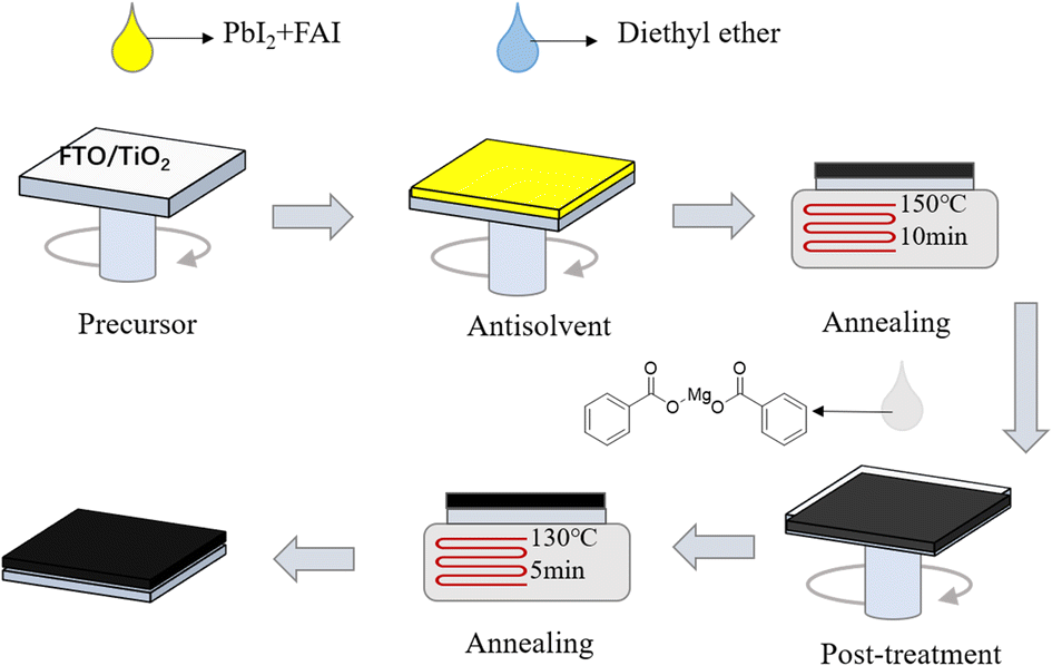 | ||
| Fig. 1 Schematic diagram of perovskite solar cell preparation process. | ||
To explore the influence of various concentrations of MgBEN on the lattice quality of the perovskite film, we utilized X-ray diffraction (XRD) to characterize. Fig. 2a displays the XRD patterns of the perovskite films, we could see two dominant peaks, corresponding to (100) and (200) diffraction indexes, respectively, and no peak was found at about 11.6°, which represents δ-phase.35 Compared to the control film, all concentrations showed an enhanced diffraction intensity at two dominant peaks (no distinct peaks shifted and no additional peaks generated), suggesting the better crystallinity of the perovskite film.36 The full width at half-maximum (FWHM) of the (100) peak drops from 0.104 to 0.099 after MgBEN modification, as depicted in Fig. S1,† also demonstrating that the modification validly improves the crystallinity of perovskite.31 The better the crystallinity of the film, the fewer nonradiative charge recombination centers, this is conducive to boosting VOC.37 Lattice strain was strictly correlated with the augmented non-radiative recombination and defect concentration, which contributes detrimentally to device performance.38–40 Using Williamson–Hall (WH) plots (individual plots for different concentrations are shown in Fig. S2†), it was found that the lattice strain of the perovskite films decreased with the 1 mM MGBEN modification, which is accountable for the reduced nonradiative recombination and enhanced carrier lifetime.35
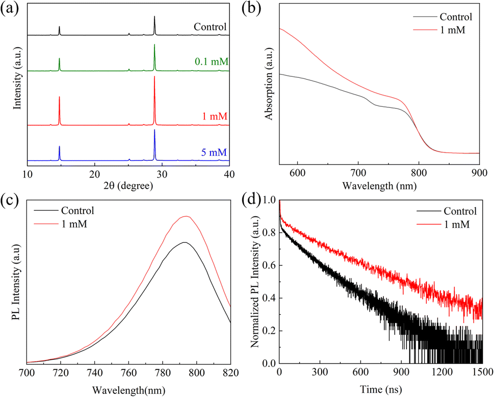 | ||
| Fig. 2 (a) The XRD patterns, (b) UV-vis absorption spectra, (c) the steady PL spectra, and (d) the TRPL spectra of the control and 1 mM MgBEN-modified perovskite films. | ||
In Fig. 2b, the Ultraviolet-visible (UV-vis) absorption spectra of the 1 mM MgBEN-modified and control perovskite films were used to further analyse the difference of light absorption properties (absorption spectra of other concentrations treated perovskite films as depicted in Fig. S3†). Obviously, after modification, the film showed the higher absorption over the entire wavelength compared to the control film with similar absorption edges. The enhanced absorbance after modification is mainly due to the formation of better perovskite film.41,42 Furthermore, as shown in Fig. S4,† we used Tauc plot to calculate the optical bandgap of control and MgBEN-modified perovskite films. We found that the bandgap was increased from 1.514 eV to 1.519 eV. However, the JSC did not become smaller, but larger. Thus, the increase in JSC may be due to a reduction in charge accumulation, which promotes carrier transport and then reduces the non-radiative recombination.
To investigate the influence of MgBEN modification on the charge carrier dynamics and recombination, we measured the steady-state photoluminescence (PL) and time-resolved photoluminescence (TRPL). Fig. 2c shows that the PL intensity of the MgBEN-modified film is stronger than the control film, which signifies the decrease of trapping centers and the suppression of nonradiative recombination43 after the modification. As shown in Fig. 2d, the corresponding TRPL spectra of control and MgBEN-modified perovskite films were fitted with a bi-exponential equation44
 | (1) |
 | (2) |
The fitted parameters are presented in Table 1. Compared with the control perovskite film (τave = 157.43 ns), the MgBEN-modified perovskite film displays a longer average carrier lifetime of 288.94 ns. Meanwhile, the τave of films treated by the other concentrations also increases (see Table S1†). The elongated lifetime demonstrates that the modification of MgBEN can significantly inhibit nonradiative recombination, consistent with the above WH plots analysis.
| A1 (%) | τ1 (ns) | A2 (%) | τ2 (ns) | τave (ns) | |
|---|---|---|---|---|---|
| Control | 71.09 | 1.62 | 28.91 | 161.28 | 157.43 |
| 1 mM | 56.72 | 3.40 | 43.28 | 293.28 | 288.94 |
We measured scanning electron microscopy (SEM) images of perovskite films to investigate the MgBEN-modified perovskite films' surface morphology. Fig. 3a and b display top-view SEM images of the control FAPbI3 films and with 1 mM MgBEN modification films. Compared to the control perovskite film, the modified film displays a better morphology with clearly increase in grain size. To quantitatively analyse the change in the grain size, the average size was calculated based on the SEM images. The distribution visually illustrates that the average grain size increased from 1.18 μm to 1.61 μm, and the maximum grain size of MgBEN-modified film was up to 2.3 μm, as shown in the Fig. 3c and d. The above results prove that the modification of MgBEN can effectively improve the quality of perovskite film, this is favourable for the photovoltaic performances and stability of the solar cells.37 Images and size distribution modified by other concentrations are shown in Fig. S6.† When the observed scale is 1 μm, we found that the grains of the 1 mM MgBEN-modified film were more closely connected, which may suppress the non-radiative recombination at the grain boundaries and facilitate the carrier transport. Corresponding SEM images are shown in Fig. S7.† As depicted in Fig. S8,† we tested the EDS of the MgBEN-modified films and found a small amount of Mg, indicating that MgBEN was effectively attached to the perovskite films. To verify whether the MgBEN surface modification affects the thickness of the perovskite layer, we made a perovskite cross-section based on the TiO2 layer and found that the thickness of the perovskite layer did not change significantly. As shown in Fig. S9.†
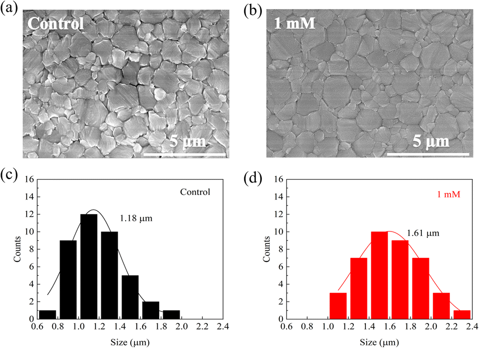 | ||
| Fig. 3 Top-view SEM images of (a) the control and (b) 1 mM MgBEN-modified perovskite films, and histograms of grain size distributions of (c) the control and (d) 1 mM MgBEN-modified perovskite films, respectively. | ||
To understand the effect of the MgBEN modification on photovoltaic performance, we fabricated devices with the abovementioned structure in the air with 30–45% humidity, as shown in Fig. 4a. Fig. 4b displays the typical current–voltage (J–V) curves of the devices treated with different concentrations of MgBEN, and the respective photovoltaic parameters are summarized in Table 2. Obviously, the photovoltaic performances increased after being modified by MgBEN. Notably, the champion device obtained a maximum PCE of 22.24% under 1 mM MgBEN concentration, with a FF of 79.33%, a VOC of 1.07 V, and a JSC of 26.09 mA cm−2. The control device exhibited a PCE of 19.94%, a FF of 79.25%, a VOC of 1.01 V, and a JSC of 24.80 mA cm−2. We found that, apart from enhanced VOC, the increased PCE of devices was mainly attributed to better JSC, probably due to the modified perovskite film becoming more conductive to charge carriers.46
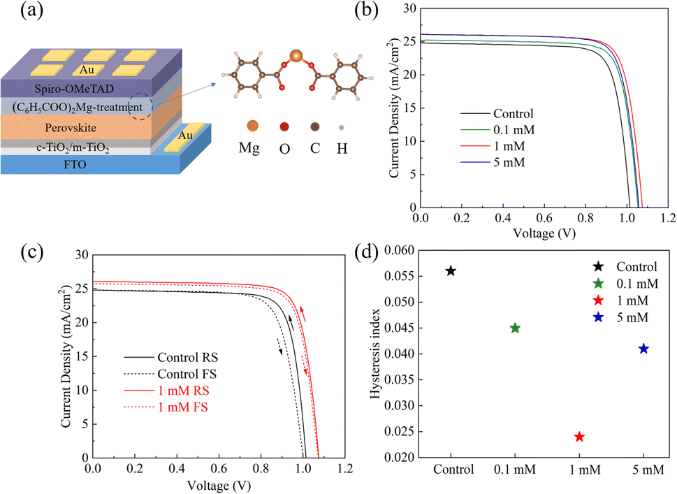 | ||
| Fig. 4 (a) Device structure with MgBEN modification, (b) J–V curves of the devices based on control and different concentrations of MgBEN modification, (c) J–V curves of the champion cells (control and 1 mM MgBEN modification), and (d) hysteresis index of different concentrations of MgBEN modification. | ||
| Samples | Scan direction | VOC (V) | JSC (mA cm−2) | FF (%) | PCE (%) | HI |
|---|---|---|---|---|---|---|
| Control | Forward | 1.00 | 24.81 | 75.93 | 18.83 | 0.056 |
| Reverse | 1.01 | 24.80 | 79.25 | 19.94 | ||
| 0.1 mM | Forward | 1.02 | 25.23 | 78.23 | 20.18 | 0.045 |
| Reverse | 1.05 | 25.24 | 79.46 | 21.13 | ||
| 1 mM | Forward | 1.07 | 25.75 | 78.65 | 21.71 | 0.024 |
| Reverse | 1.07 | 26.09 | 79.33 | 22.24 | ||
| 5 mM | Forward | 1.05 | 25.13 | 79.38 | 20.94 | 0.041 |
| Reverse | 1.06 | 26.10 | 79.11 | 21.84 |
Meanwhile, the hysteresis was an important issue in the PSCs, it was related to the ion migration and trap states, and the hysteresis index (HI) of the device was calculated according to the following equation47
 | (3) |
Here, the hysteresis characteristics were obtained by using different scan directions (reverse scanning (RS), forward scanning (FS)), and the results were depicted in Fig. 4c. Table 2 and Fig. 4d demonstrate that HI values depend on the scan direction. We found that the HI values of MgBEN-modified devices significantly reduced from 0.056 (for the control device) to 0.024, suggesting better carrier transport and collection which accounted for the synergistic effect of defect passivation and grain size increase.48
In order to avoid experimental contingency, we tested 20 sets of data for each simple. Fig. 5 displays the statistical JSC, VOC, FF, and PCE for the control and different concentrations of MgBEN. We found that the modification of 1 mM MgBEN substantially improves VOC and JSC, leading to a better PCE. Compared to the control and other concentrations, the data of 1 mM MgBEN modification has smaller dispersion of photovoltaic parameters of VOC and FF, and relatively smaller JSC. Although PCE has the largest dispersion, its minimum is the highest, which also indicates that 1 mM MgBEN has a better modification effect than control and other concentrations.
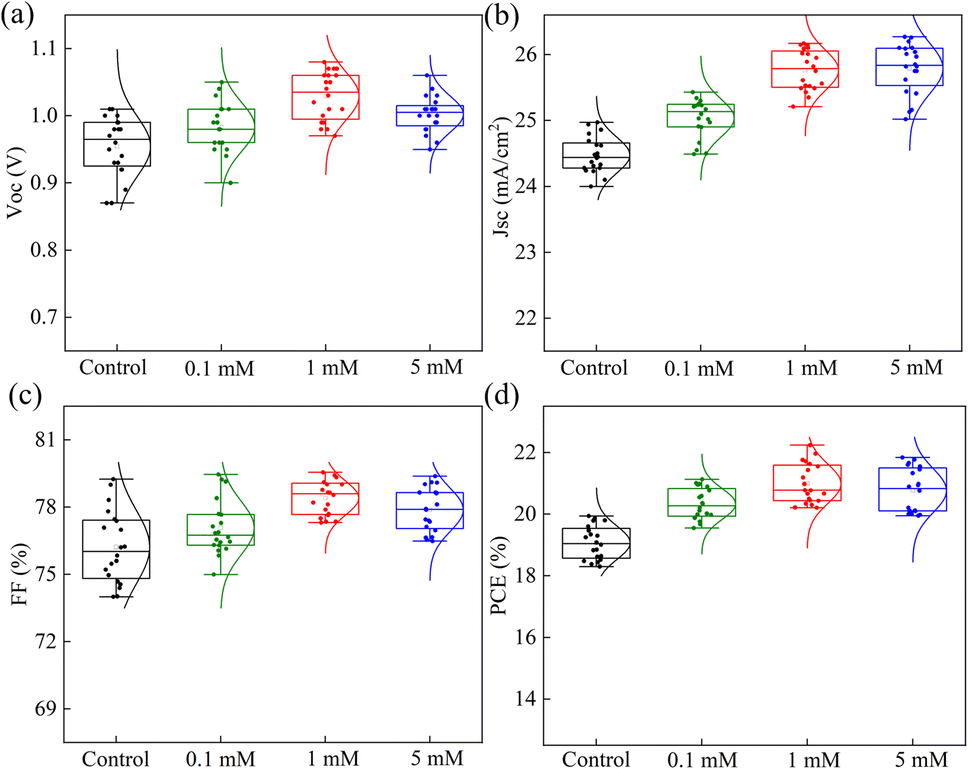 | ||
| Fig. 5 Statistical photovoltaic parameters of (a) VOC, (b) JSC, (c) FF, and (d) PCE. | ||
We suggested a probable mechanism for the passivation of FAPbI3 surface defects by MgBEN in Fig. 6 and explained as follows: C6H5COOMg+ could fill A site (VFA), meanwhile, it can form a more likely covalent with I−, which can effectively prevent the migration of cations at the A site. Based on previous studies,49 compared to Cl−, Br−, I− and BF4−, HCOO− has the highest binding energy to I− vacant sites. C6H5COO−, the homologue of HCOO− was introduced here, allowing for the similar passivation of the X sites.
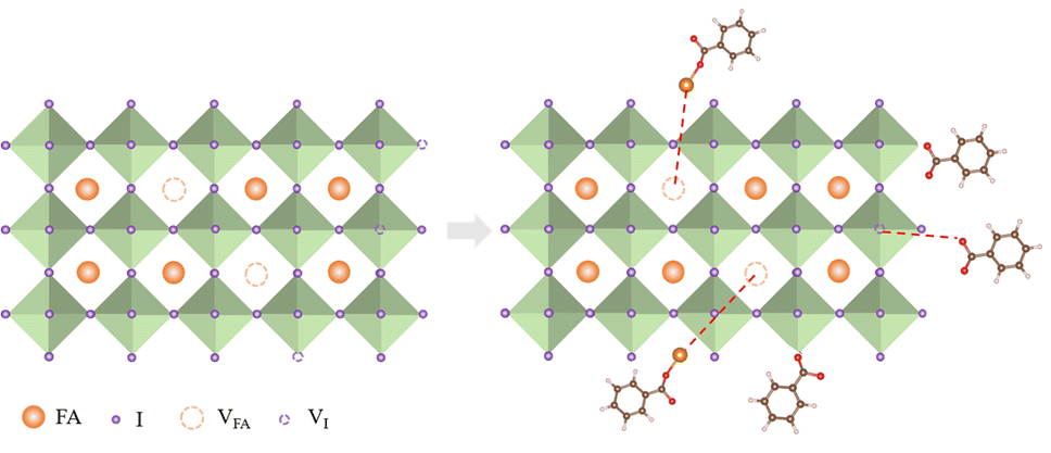 | ||
| Fig. 6 Mechanism diagram of synergistic passivation of A and X sites by MgBEN on the surface of perovskite films. | ||
At present, stability is still a major challenge for the commercialization of PSCs.50 To confirm the influence of the MgBEN modification on the stability of perovskite, we tracked the long-term stability of devices stored in dry air (RH: 20–30%). As shown in Fig. 7a, compared to the control, in the 30 days test, the modified MgBEN still exceeded 90% of the original PCE. In addition to this, steady-state PL spectra were measured every ten minutes to investigate the stability of perovskite films. As depicted in Fig. 7c, the PL intensity of MgBEN-modified perovskite film remained virtually unchanged, and only decayed slightly during the first 10 minutes. In contrast, the PL intensity of the control perovskite film, as shown in Fig. 7b, experienced a significant decay within 50 minutes. This indicates that nonradiative recombination is significantly suppressed, suggesting a remarkably reduced trap state in the MgBEN-modified perovskite film.
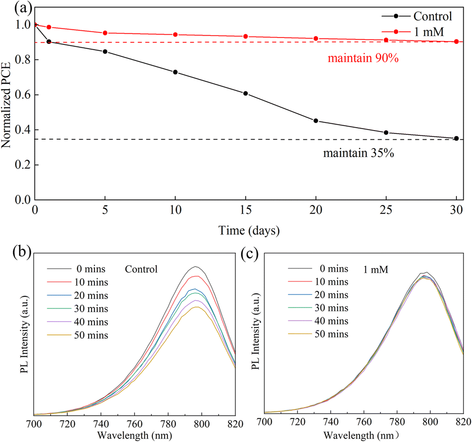 | ||
| Fig. 7 Device stability measured at room temperature in dry air with 30–40% humidity within 30 days (a). And variations in photoluminescence were tested every ten mins within 50 min of the control perovskite film (b) and that of 1 mM MgBEN-modified perovskite film (c). | ||
Conclusions
In short, we have demonstrated a simple defect passivation method by passivating MgBEN on perovskite film. We found that the MgBEN treatment increased grain size, improved the film quality and decreased lattice strain, contributing to the enhanced carrier transport and reduction of non-radiative recombination. The champion device prepared with MgBEN passivation obtained a PCE of 22.24% with negligible hysteresis due to the synergistic passivation of the A and X sites. More importantly, the MgBEN modification remarkably increased the perovskite film stability. The corresponding PSCs preserved nearly 90% of the original PCE, while the PCE of the untreated devices kept only 35% of the initial within 30 days (RH: 20–30%). Our study offers a new strategy to fabricate highly efficient and stable PSCs.Experimental
Materials
Titanium(diisopropoxide) bis(2,4-pentanedionate) (75%, Macklin), n-Butanol (99.8%, Aladdin). Methylammonium chloride (MACl, 99.5%), formamidinium iodide (FAI), lead iodide (PbI2), spiro-OMeTAD, Li-TFSI, FK209 were purchased from Xi'an p-OLED. chlorobenzene (CB), 4-tert-butyl pyridine (tBP). Magnesium benzoate ((C6H5COO)2Mg) were purchased from Sigma-Aldrich. Dimethyl sulfoxide (DMSO) (99.9% Macklin) and dimethylformamide (DMF) (99.9%, Macklin).Device fabrication
FTO substrates were treated by deionized water, decon90, isopropanol, ethyl alcohol, and deionized water three times for 20 min sequentially. Then, they were be dried in an oven at 100 °C and treated with 30 min ultraviolet ozone. The compact titanium dioxide layer (c-TiO2), was spin-coated using diisopropoxy bis(acetylacetonate) titanium solution into n-butanol (1![[thin space (1/6-em)]](https://www.rsc.org/images/entities/char_2009.gif) :16, V/V) at 2000 rpm for 45 s and annealed in an oven at 120 °C for 15 min. After cooled down, the mesoscopic TiO2 layer (m-TiO2) was spin-coated at 5000 rpm for 10 s and calcined at 500 °C for 60 min. The mesoscopic TiO2 solution needs to prepare 24 hours in advance, diluted TiO2 paste with ethanol, mass ratio of 1:8.
:16, V/V) at 2000 rpm for 45 s and annealed in an oven at 120 °C for 15 min. After cooled down, the mesoscopic TiO2 layer (m-TiO2) was spin-coated at 5000 rpm for 10 s and calcined at 500 °C for 60 min. The mesoscopic TiO2 solution needs to prepare 24 hours in advance, diluted TiO2 paste with ethanol, mass ratio of 1:8.
In an N2 glove box, perovskite precursor solution was obtained with PbI2 and FAI and MACl in a mixture of DMSO and DMF solvents (molar ratio of DMF/DMSO = 4:1). Then, the FAPbI3 solution was coated on the m-TiO2 substrate and spined at 1000 rpm for 18 s and 4000 rpm for 28 s. In the second stage of the spin-coating (high speed) process, the antisolvent (1 ml of diethyl ether) was dumped on the substrate after the first 8 s, then after 20 seconds of vacuum treatment in a chamber with a pressure of less than 0.1 Pa, the substrate was transferred to a hot plate at 150 °C for 10 min with 35–45% humidity ambient conditions. Mg(C6H5COO)2 was dissolved in ethyl alcohol, then 100 μL solution spin-coated on the substrate at 3000 rpm for 10 s, subsequently annealed at 130 °C for 5 min. After the films cooling down to room temperature, 40 μL Spiro-OMeTAD solution was spin-coated on the substrate at 3000 rpm for 30 s. Finally, 80 nm gold electrode was deposited on the substrate by thermal vacuum evaporation.
Characterization
The PL and TRPL spectra (PicoQuanT GmbH, FluoTime 300) were obtained by time-single setting under an excitation source at 650 nm. XRD spectra were recorded with a scan range of 10–50° for 5° per minute. The UV-Vis absorption spectra (UV-3600) were measured from 300 to 900 nm. The perovskite film surface was examined by SEM (HITACHI, S-4800) to investigate grain size, then analyzed surface elemental content by EDS. The grain size contribution of perovskite was analyzed by Nano measurer 1.2 software. A solar simulator (Sol3A Newport) was used to capture the J–V curves of the PSCs. The source was equipped with a xenon lamp (450 W) that simulated AM 1.5 G of sunlight with an optical density of 100 mW cm−1−2, calibrated by using a standard silicon cell.Conflicts of interest
There are no conflicts to declare.Acknowledgements
This work was supported by Nanxin Pharm Co., Ltd, Nanjing.Notes and references
- H. S. Kim, C. R. Lee, J. H. Im, K. B. Lee, T. Moehl, A. Marchioro, S. J. Moon, R. Humphry-Baker, J. H. Yum, J. E. Moser, M. Grätzel and N. G. Park, Sci. Rep., 2012, 2, 591 CrossRef PubMed
.
- A. Kojima, K. Teshima, Y. Shirai and T. Miyasaka, J. Am. Chem. Soc., 2009, 131, 6050–6051 CrossRef CAS PubMed
- Y. Wang, D. Yang, X. Zhou, S. M. Alshehri, T. Ahamad, A. Vadim and D. Ma, J. Mater. Chem. C, 2016, 4, 7415–7419 RSC
- H. Zhang, Y. Xiao, F. Qi, P. Liu, Y. Wang, F. Li, C. Wang, G. Fang and X. Zhao, ACS Sustainable Chem. Eng., 2019, 7, 8236–8244 CrossRef CAS
- Z. Shi, Y. Li, S. Li, X. Li, D. Wu, T. Xu, Y. Tian, Y. Chen, Y. Zhang, B. Zhang, C. Shan and G. Du, Adv. Funct.Mater., 2018, 28, 1707031 CrossRef
- J. Huang, Y. Yuan, Y. Shao and Y. Yan, Nat. Rev. Mater., 2017, 2, 17042 CrossRef CAS
- H. D. Pham, L. Xianqiang, W. Li, S. Manzhos, A. K. K. Kyaw and P. Sonar, Energy Environ. Sci., 2019, 12, 1177–1209 RSC
- D. B. Khadka, Y. Shirai, M. Yanagida, T. Noda and K. Miyano, ACS Appl. Mater. Interfaces, 2018, 10, 22074–22082 CrossRef CAS PubMed
- E. J. Juarez-Perez and M. Haro, Science, 2020, 368, 1309 CrossRef CAS PubMed
- https://www.nrel.gov/pv/cell-efficiency.html, accessed on October 20, 2022.
- J. Chen and N.-G. Park, Adv. Mater., 2019, 31, 1803019 CrossRef CAS PubMed
- N. Li, X. Niu, Q. Chen and H. Zhou, Chem. Soc. Rev., 2020, 49, 8235–8286 RSC
- S.-W. Kim, G. Kim, C. S. Moon, T.-Y. Yang and J. Seo, Small Methods, 2021, 5, 2001248 CrossRef CAS PubMed
- B. Li, V. Ferguson, S. R. P. Silva and W. Zhang, Adv. Mater. Interfaces, 2018, 5, 1800326 CrossRef
- H. Xu, Y. Miao, N. Wei, H. Chen, Z. Qin, X. Liu, X. Wang, Y. Qi, T. Zhang and Y. Zhao, Adv. Energy Mater., 2021, 12, 2103151 CrossRef
- J. Jeong, M. Kim, J. Seo, H. Lu, P. Ahlawat, A. Mishra, Y. Yang, M. A. Hope, F. T. Eickemeyer, M. Kim, Y. J. Yoon, I. W. Choi, B. P. Darwich, S. J. Choi, Y. Jo, J. H. Lee, B. Walker, S. M. Zakeeruddin, L. Emsley, U. Rothlisberger, A. Hagfeldt, D. S. Kim, M. Gratzel and J. Y. Kim, Nature, 2021, 592, 381–385 CrossRef CAS PubMed
- W. Hui, L. Chao, H. Lu, F. Xia, Q. Wei, Z. Su, T. Niu, L. Tao, B. Du, D. Li, Y. Wang, H. Dong, S. Zuo, B. Li, W. Shi, X. Ran, P. Li, H. Zhang, Z. Wu, C. Ran, L. Song, G. Xing, X. Gao, J. Zhang, Y. Xia, Y. Chen and W. Huang, Science, 2021, 371, 1359–1364 CrossRef CAS PubMed
- Q. Jiang, Y. Zhao, X. Zhang, X. Yang, Y. Chen, Z. Chu, Q. Ye, X. Li, Z. Yin and J. You, Nat. Photonics, 2019, 13, 460–466 CrossRef CAS
- Z. Xiong, X. Chen, B. Zhang, G. O. Odunmbaku, Z. Ou, B. Guo, K. Yang, Z. Kan, S. Lu, S. Chen, N. A. N. Ouedraogo, Y. Cho, C. Yang, J. Chen and K. Sun, Adv. Mater., 2022, 34, e2106118 CrossRef PubMed
- Q. Zhuang, C. Zhang, C. Gong, H. Li, H. Li, Z. Zhang, H. Yang, J. Chen and Z. Zang, Nano Energy, 2022, 102, 107747 CrossRef CAS
- X. Wu, B. Li, Z. Zhu, C. C. Chueh and A. K. Jen, Chem. Soc. Rev., 2021, 50, 13090–13128 RSC
- Z. Cheng, C. Gao, J. Song, D. Ding, Y. Chen, J. Wang, D. Zhang, L. Chen, X. Wang, Z. Yang, F. Liu, H. Liu and W. Shen, ACS Appl. Mater. Interfaces, 2021, 13, 40778–40787 CrossRef PubMed
- Z. Liu, F. Cao, M. Wang, M. Wang and L. Li, Angew. Chem., Int. Ed., 2020, 59, 4161–4167 CrossRef CAS PubMed
- S. Wang, H. Cao, X. Liu, Y. Liu, T. Tao, J. Sun and M. Zhang, ACS Appl. Mater. Interfaces, 2020, 12, 3661–3669 CrossRef CAS PubMed
- Z. Li, B. Li, X. Wu, S. A. Sheppard, S. Zhang, D. Gao, N. J. Long and Z. Zhu, Science, 2022, 376, 416–420 CrossRef CAS PubMed
- K. Zou, Q. Li, J. Fan, H. Tang, L. Chen, S. Tao, T. Xu and W. Huang, ACS Mater. Lett., 2022, 4, 1101–1111 CrossRef CAS
- W. Zhang, L. He, Y. Meng, H. Kanda, D. Tang, B. Ding, Y. Ding, M. K. Nazeeruddin and X. Li, Adv. Energy Mater., 2022, 12, 2202189 CrossRef CAS
- N. Ma, J. Jiang, G. Wang, D. Wang, Y. Zhang, Y. Wang, Y. Wang, Y. Ji, W. Wei and L. Shen, ACS Appl. Mater. Interfaces, 2021, 13, 44401–44408 CrossRef CAS PubMed
- J. Guo, J. Sun, L. Hu, S. Fang, X. Ling, X. Zhang, Y. Wang, H. Huang, C. Han, C. Cazorla, Y. Yang, D. Chu, T. Wu, J. Yuan and W. Ma, Adv. Energy Mater., 2022, 12, 2200537 CrossRef CAS
- Y. Liu, H. Cao, X. Liu, R. Zhu, T. Tao and J. J. N. Sun, Nanotechnology, 2021, 32, 355201 CrossRef CAS PubMed
- Z. Liu, F. Cao, M. Wang, M. Wang and L. Li, Angew. Chem., Int. Ed., 2020, 59, 4161–4167 CrossRef CAS PubMed
- K. Fajans, Struktur und Deformation der Elektronenhullen in ihrer Bedeutung fur die chemischen und optischen Eigenschaften anorganischer Verbindungen, Naturwissenschaften, 1923, 11, 165–172 CrossRef CAS
- M. Lyu, D.-K. Lee and N.-G. J. N. H. Park, Nanoscale Horiz., 2020, 5, 1332–1343 RSC
- A. R. b. Mohd Yusoff, M. Vasilopoulou, D. G. Georgiadou, L. C. Palilis, A. Abate and M. K. Nazeeruddin, Energy Environ. Sci., 2021, 14, 2906–2953 RSC
- G. Kim, H. Min, K. S. Lee, D. Y. Lee, S. M. Yoon and S. I. Seok, Science, 2020, 370, 108–112 CrossRef CAS PubMed
- H. Zheng, G. Liu, W. Wu, H. Xu and X. Pan, ChemSusChem, 2021, 14, 3147–3154 CrossRef CAS PubMed
- R. Zhao, T. Wu, R. Zhuang, Y. Hua and Y. Wang, Energy Environ. Mater., 2022, e12417 Search PubMed
- T. W. Jones, A. Osherov, M. Alsari, M. Sponseller, B. C. Duck, Y.-K. Jung, C. Settens, F. Niroui, R. Brenes, C. V. Stan, Y. Li, M. Abdi-Jalebi, N. Tamura, J. E. Macdonald, M. Burghammer, R. H. Friend, V. Bulović, A. Walsh, G. J. Wilson, S. Lilliu and S. D. Stranks, Energy Environ. Sci., 2019, 12, 596–606 RSC
- D.-J. Xue, Y. Hou, S.-C. Liu, M. Wei, B. Chen, Z. Huang, Z. Li, B. Sun, A. H. Proppe, Y. Dong, M. I. Saidaminov, S. O. Kelley, J.-S. Hu and E. H. Sargent, Nat. Commun., 2020, 11, 1514 CrossRef CAS PubMed
- C. Zhu, X. Niu, Y. Fu, N. Li, C. Hu, Y. Chen, X. He, G. Na, P. Liu, H. Zai, Y. Ge, Y. Lu, X. Ke, Y. Bai, S. Yang, P. Chen, Y. Li, M. Sui, L. Zhang, H. Zhou and Q. Chen, Nat. Commun., 2019, 10, 1–11 CrossRef PubMed
- C. Liu, S. Liu, Y. Wang, Y. Chu, K. Yang, X. Wang, C. Gao, Q. Wang, J. Du, S. Li, Y. Hu, Y. Rong, L. Guo, A. Mei and H. Han, Adv. Funct.Mater., 2021, 31, 2010603 CrossRef CAS
- G. Liu, H. Zheng, J. Ye, S. Xu, L. Zhang, H. Xu, Z. Liang, X. Chen and X. Pan, ACS Energy Lett., 2021, 6, 4395–4404 CrossRef CAS
- Q. Zhou, Y. Gao, C. Cai, Z. Zhang, J. Xu, Z. Yuan and P. Gao, Angew. Chem., Int. Ed., 2021, 60, 8303 CrossRef CAS PubMed
- J. Chen, X. Zhao, S.-G. Kim and N.-G. Park, Adv. Mater., 2019, 31, 1902902 CrossRef PubMed
- J. Chen, S.-G. Kim and N.-G. Park, Adv. Mater., 2018, 30, 1801948 CrossRef PubMed
- W. Sun, M. Zhang, S. Wang, F. Cao, J. Zou, Y. Du, Z. Lan and J. Wu, J. Mater. Chem. C, 2021, 9, 7726–7733 RSC
- W. Li, M. U. Rothmann, Y. Zhu, W. Chen, C. Yang, Y. Yuan, Y. Y. Choo, X. Wen, Y.-B. Cheng, U. Bach and J. Etheridge, Nat. Energy, 2021, 6, 624–632 CrossRef CAS
- G. Xia, B. Huang, Y. Zhang, X. Zhao, C. Wang, C. Jia, J. Zhao, W. Chen and J. Li, Adv. Mater., 2019, 31, 1902870 CrossRef PubMed
- J. Jeong, M. Kim, J. Seo, H. Lu, P. Ahlawat, A. Mishra, Y. Yang, M. A. Hope, F. T. Eickemeyer, M. Kim, Y. J. Yoon, I. W. Choi, B. P. Darwich, S. J. Choi, Y. Jo, J. H. Lee, B. Walker, S. M. Zakeeruddin, L. Emsley, U. Rothlisberger, A. Hagfeldt, D. S. Kim, M. Grätzel and J. Y. Kim, Nature, 2021, 592, 381–385 CrossRef CAS PubMed
- G. Nazir, S.-Y. Lee, J.-H. Lee, A. Rehman, J.-K. Lee, S. I. Seok and S.-J. Park, Adv. Mater., 2022, 34, 2204380 CrossRef CAS PubMed
Footnote |
| † Electronic supplementary information (ESI) available. See DOI: https://doi.org/10.1039/d2ra06761g |
| This journal is © The Royal Society of Chemistry 2023 |