
 Open Access Article
 This Open Access Article is licensed under a Creative Commons Attribution-Non Commercial 3.0 Unported Licence
Half-metallic antiferromagnets induced by non-magnetic adatoms on bilayer silicene
Xiao-Fang Ouyang *a,
Yu-Zhong Zhang*b,
Lu Wanga and
De-Sheng Liuc
*a,
Yu-Zhong Zhang*b,
Lu Wanga and
De-Sheng Liuc
aSchool of Physics and Electrical Information, Shangqiu Normal University, Henan 476000, P. R. China. E-mail: oyxf328@126.com
bShanghai Key Laboratory of Special Artificial Microstructure Materials and Technology, School of Physics Science and Engineering, Tongji University, Shanghai 200092, P. R. China. E-mail: yzzhang@tongji.edu.cn
cSchool of Energy and Machinery Engineering, Jiangxi University of Science and Technology, Nanchang 330013, P. R. China
First published on 16th January 2023
Abstract
Transition metal-free magnetism and two-dimensional p-state half-metals have been a fascinating subject of research due to their potential applications in nanoelectronics and spintronics. By applying density functional theory calculations, we predict that bilayer silicene can be an interlayer antiferromagnetic ground state. Interestingly, the half-metallicity is realized by adsorbing non-magnetic atoms on the antiferromagnetic bilayer silicene in the absence of transition magnetic atoms, nanoribbons, ferromagnetic substrates and magnetic field. Then, on the basis of first principles calculations and theoretical analysis, we show that the realization of half-metallicity is induced by the split of antiferromagnetic degeneracy due to the localization of transfer charge from the adatom to silicene. Our findings may open a new avenue to silicene-based electronic and spintronic devices.
I. Introduction
Spintronics aims to utilize the spin degree of freedom, in addition to the electrical charge, and perform memory and logic operations in electronic devices.1 Due to the extraordinary physical properties,2,3 emerging two-dimensional (2D) materials have become important candidates for the next-generation low-power spintronic devices and nano devices. However, spintronic applications of 2D materials are impeded due to their intrinsic non-magnetism.4 Hence, ferromagnetism of 2D materials has been an enduring topic in the field. Generally, the traditional approach of achieving ferromagnetic order and half-metallicity in graphene is to introduce defects,5 impurities,6–8 hybrid structure,9 nanoribbons10,11 and surface functionalization.12 However, the distributions of dopants or defects cannot be easily controlled experimentally,13,14 and so may not be practical. In order to overcome this problem, much effort has been made to investigate intrinsic two-dimensional ferromagnets and half-metals.15–20 Nevertheless, transition-metal-containing systems may not be compatible with many current mature technologies, which mainly rely on a main group semiconductor. Moreover, the strong spin coupling of d electrons results in a short spin relaxation time and lower carrier mobility compared with p-state semiconductors. Besides, the microscopic-ferromagnetism arising from magnetic atoms is not immune to external magnetic fields, which is unfavorable for application in nano devices. These above problems may be resolved by p-state two-dimensional half-metals (PTDHMS), in which the 100% spin polarization and zero macromagnetism can coexist.21 In fact, theoretically reported PTDHMS, such as g-C4N3,22 YN2,23 g-C14N12,24 and C6N7,25 have a much smaller Fermi velocity compared with graphene and silicene. Moreover, these reported PTDHMS are theoretically incompatible with current silicon (Si)-based electronic technology. Hence, developing PTDHMS based on Si materials is significant for practical application in nanoelectric devices.Si-based half-metals have attracted great attention due to the Dirac cone,26 long spin-diffusion time and spin coherence length,27,28 and low-power consumption as well as integrating with current Si-based semiconductor technology. To date, some Si-based half-metals have been theoretically proposed. For example, the half-metallicity could be realized in zigzag silicene nanoribbons by substituting Si with the N atom,29 edge hydrogenation30 or by Al/P co-doping.31,32 Nevertheless, it remains unpractical experimentally due to complex technology such as the strong in-plane electric field30,33,34 or fine modification in the nanoribbons.35,36 Furthermore, the superior physical properties will no longer exist in edge modified systems. Hence, instead of silicene nanoribbons, silicene nanosheets with half-metallic nature are more attractive. Theoretically, it has been proven that the half-metallicity is achieved in silicene nanosheets by adsorption of transition metal atoms such as Cr or Mn;37 unfortunately, the half-metallic gap is almost negligible. Moreover, magnetic doping tends to form clusters, resulting in enhanced scattering, which impedes such applications. On the other hand, the stray field arising from ferromagnets may be harmful in highly integrated circuits.38 Therefore, the Si-based half-metals without macroscopic ferromagnetism attract extensive attention. Although half-metallicity can be achieved by full nitrogenation on one Si sublattice, it is difficult to operate experimentally.39 The half-metallic antiferromagnets as a subclass of half-metals have the advantage of fully spin-polarized current while exhibiting zero macroscopic magnetization.40 Hence, the search for half-metal antiferromagnets based on silicene is of great importance for both fundamental interest and devices.
In this paper, we systematically explore the electronic structures and magnetic properties of bilayer silicene with non-magnetic adatoms by first-principles calculations. The antiferromagnetic ground state with interlayer antiferromagnetism and intralayer ferromagnetism is confirmed by the electronic structures and phonon calculations.41 With the action of adatoms, the half-metallicity without ferromagnetic substrate/magnetic field/magnetic ions, cutting silicene into nanoribbons, or selective modification like semihydrogenation/nitrogenation and spin–orbital coupling, is realized. We reveal that localization of electrons introduced by adatoms splits the antiferromagnetic degeneracy of the sublattice, resulting in the half-metallicity, which may be obtained by deposing non-magnetic atoms on antiferromagnetic materials. Our results derived from antiferromagnetic silicene highlight a new promising avenue toward realistic transition metal-free spintronics applications.
Our paper is organized as follows: Section II describes the details of the methods we used. Section III presents our main results and discussion, including the electronic structures of the different adsorption systems, density of states (DOS), results of molecular dynamics calculations, contour maps of charge density difference (CDD) and spin density difference (SDD). Section IV concludes with a summary.
II. Methods
The structural optimization and electronic structure are all performed based on the projector augmented wave method,42 as implemented in the Vienna Ab initio Simulation Package (VASP).43,44 We chose the generalized gradient approximation (GGA) of Perdew–Burke–Ernzerhof45 for the exchange–correlation potentials. A plane-wave energy cutoff of 500 eV is employed. To check the reliability of the functional, HSE06 (ref. 46) was also applied to calculate the band structure of bilayer silicene. In the self-consistent potential, we employed a 4 × 4 × 1 unit cell with a set of 8 × 8 × 1 Monkhorst–Pack k-points grid for Brillouin-zone integration. When the density of states (DOS) is calculated, a 16 × 16 × 1 k-point sampling is used. A vacuum region of 20 Å along the c direction perpendicular to the surface is employed to avoid any artificial interactions between repeated slabs. A single adatom was added in the 4 × 4 × 1 supercell including 64 Si atoms, which yielded an adatom concentration of ∼4.19 × 1013 cm−2. All atomic positions and constants of the supercell were optimized until the atomic forces were less than 0.01 eV Å−1. For the optimized system, we define the adsorption energy as Eads = Esystem − (Esilicene + Eadatom), where Esystem, Esilicene and Eadatom are the total energies of the 4 × 4 × 1 silicene + adatom system, supercell of silicene and isolated single adatom, respectively. To verify the stability of the structure and magnetism of silicene, we performed spin-polarized molecular dynamics simulations of a 6 × 6 × 1 system including 144 atoms with a Nosé–Hoover thermostat at either 100 K or 300 K for 10![[thin space (1/6-em)]](https://www.rsc.org/images/entities/char_2009.gif) 000 fs with a time step of 2 fs.
000 fs with a time step of 2 fs.
III. Results and discussion
The bilayer silicene discussed in the present work is shown in Fig. 1(b). For the convenience of later analysis, from top to bottom, these layers are denoted as I, II, III and IV, respectively. The antiferromagnetic ground state with interlayer antiferromagnetism and intralayer ferromagnetism is verified theoretically, and calculated magnetic moments mainly exist in the atoms of the I and IV layers with −0.094 μB and 0.094 μB,41 respectively. While atoms of the II and III layers show spin up and spin down with negligible magnetic moment. This long-range antiferromagnetism between two layers has also been theoretically confirmed in other works.47,48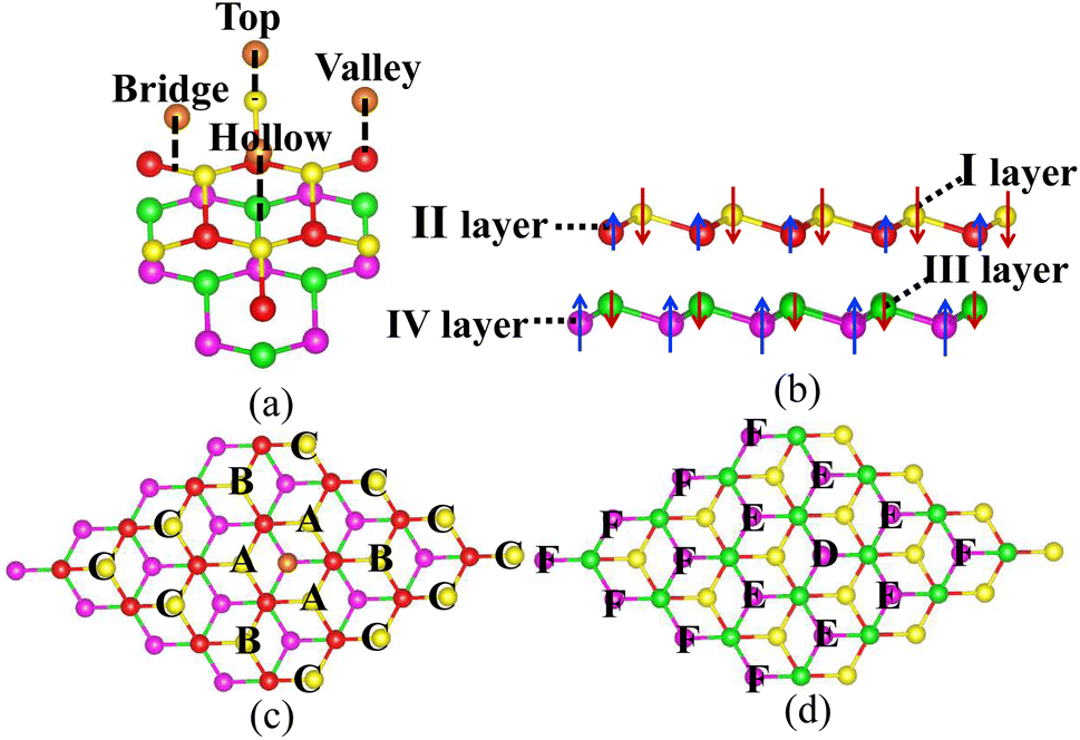 | ||
| Fig. 1 (a) Four different adsorption positions. (b) Side view of antiferromagnetic bilayer silicene; arrow represents the spin direction. (c) Front view of adsorption system. (d) Bottom view of adsorption system. | ||
To show the effect of non-magnetic adatoms on the electronic structure of bilayer silicene. The alkali metal, alkaline-earth metal, B and Al adatoms are considered. As illustrated in Fig. 1(a), four different adsorption positions such as center of hexagonal Si atoms (hollow site), on top of the upper Si atom (top site), on top of the lower Si atom (valley site), on top of the Si–Si bond (bridge site) are included. By calculating the adsorption energy, we found that all the adatoms prefer the hollow site. For the adatom, the nearest, next-nearest and outlying Si atoms of the I layer are labeled with A, B and C, respectively, as presented in Fig. 1(c). In Fig. 1(d), D, E and F indicate the nearest, next-nearest and outlying Si atoms in the IV layer, respectively. The geometric structures and electronic properties for the hollow site are summarized in Table 1. The height, defined as the average distance of the z-component between the adatom and Si atoms of the I layer, increases monotonously with increase in adatom size. Here, the z-component denotes the direction perpendicular to the silicene plane. Although there is no obvious trend in the adsorption energies, which are all greater than those in graphene49 and monolayer silicene,37 showing the stability of the adsorption system. Furthermore, the relaxed lattice constants of the adsorption systems are similar to that of pristine silicene, which confirms the operability in the experiment. The total magnetic moments (μtot shown in Table 1) show that all adsorption systems are ferromagnetic state.
| a (Å) | h (Å) | ρad (e) | Eads (eV) | μA (μB) | μB (μB) | μC (μB) | μtot (μB) | Eg (eV) | |
|---|---|---|---|---|---|---|---|---|---|
| Li | 15.469 | 1.459 | 0.87 | −2.75 | −0.014 | −0.074 | −0.074 | 0.280 | Metal |
| Na | 15.473 | 2.014 | 0.84 | −2.20 | −0.015 | −0.072 | −0.073 | 0.256 | Metal |
| K | 15.469 | 2.535 | 0.83 | −2.40 | −0.019 | −0.069 | −0.073 | 0.259 | Metal |
| Be | 15.443 | 0.909 | 1.35 | −2.80 | 0.009 | −0.066 | −0.074 | 0.668 | H-metal |
| Mg | 15.468 | 1.483 | 1.32 | −1.82 | 0.008 | −0.068 | −0.079 | 0.664 | H-metal |
| MgCa | 15.468 | 1.483 | 1.30 | −3.18 | 0.020 | −0.082 | −0.085 | 0.689 | Metal |
| Ca | 15.471 | 1.737 | 1.36 | −3.36 | 0.020 | −0.080 | −0.086 | 0.691 | S-con |
| CaMg | 15.471 | 1.737 | 1.17 | −1.81 | 0.001 | −0.072 | −0.083 | 0.648 | H-metal |
| B | 15.399 | 0.825 | −0.67 | −4.16 | 0.025 | −0.078 | −0.087 | 1.009 | Metal |
| Al | 15.455 | 1.353 | 1.22 | −3.64 | 0.025 | −0.085 | −0.089 | 0.952 | H-metal |
| Silicene | 15.44 | −0.094 | −0.094 | −0.094 | 0 | S-con | |||
| SiliceneMg | 15.468 | −0.093 | −0.098 | −0.110 | −0.004 | S-con |
For the charge transfer analysis, the effective charge on the atoms is obtained by the Bader method. In Table 1, the net charges transferred from alkali metal atoms to silicene have almost equal values of 0.8e, inducing similar μtot and band structures, as shown in Table 1 as well as Fig. 2(a)–(c). Compared with alkali metal atoms, the charge transfer from alkaline-earth metals to silicene increases due to more valence charge, while the height decreases with the decrease in atomic size. Owing to the strong electronegativity of the B atom, the charge transfers from silicene to B atom, with a value of −0.67e, as shown in Table 1.
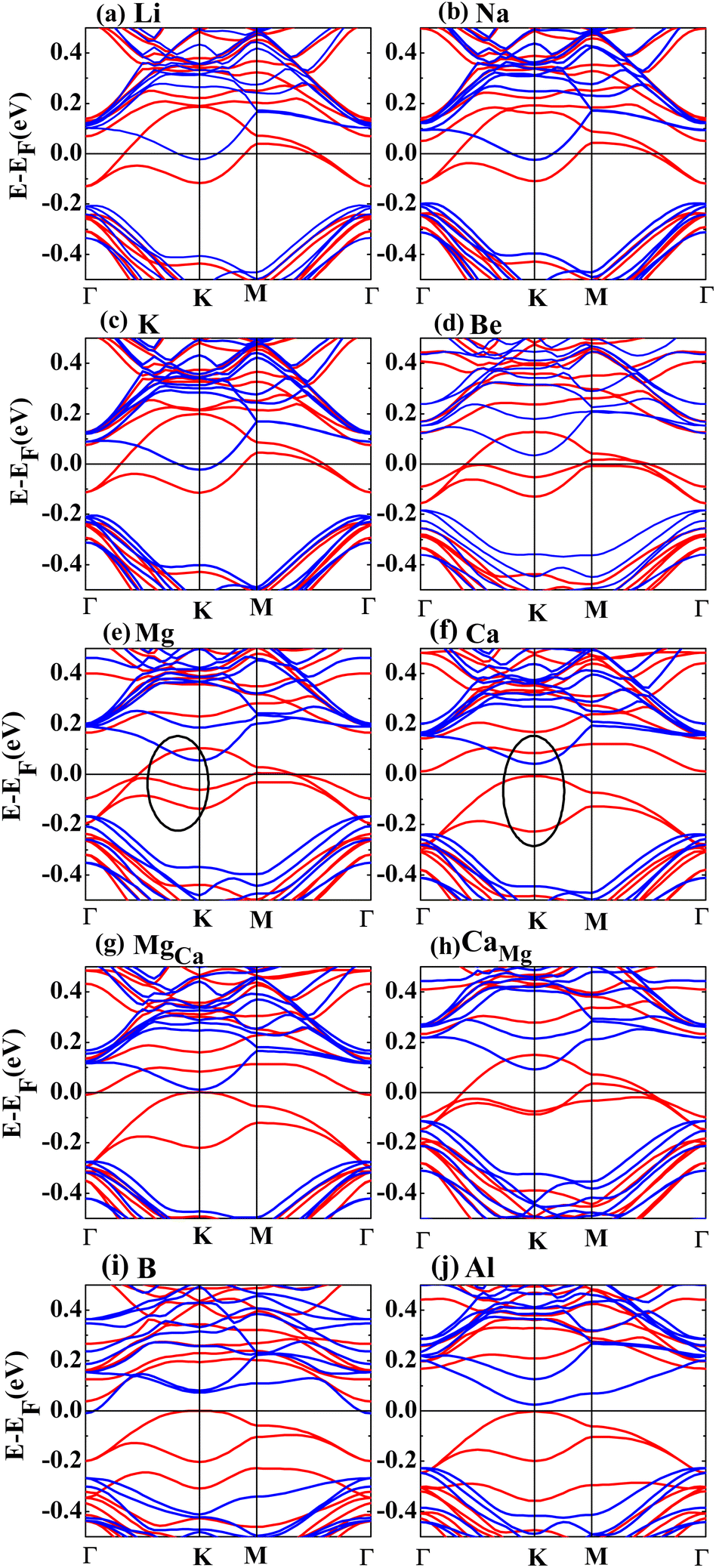 | ||
| Fig. 2 The band structures for Li (a), Na (b), K (c), Be (d), Mg (e), Ca (f), MgCa (g), CaMg (h), B (i) and Al (j) adsorbates, Fermi level is set to zero. The red and blue lines represent spin up and spin down, respectively. | ||
Fig. 2 shows the band structures of the adsorbed systems. It is found that the adsorption systems have a spin-polarized state around the Fermi level, while still remaining antiferromagnetic far away from the Fermi level. The adsorption systems with Li, Na, K and B are metal, as shown in Fig. 2(a), (b), (c) and (i), respectively. More interesting, the silicene with Be, Mg and Al prefers half-metal, as illustrated in Fig. 2(d), (e) and (j), respectively, while the Ca-adsorbed system shows semiconductor properties. In order to analyze the effect of different layers on realization of half-metal, the projected DOS are calculated, as shown in Fig. 3. For comparison, the corresponding results for pristine silicene are also calculated. Fig. 3 shows that the pristine silicene is a semiconductor, while the Fermi level moves to a higher level with the increase in electrons from the adsorbate, inducing the spin polarization. Moreover, the spin polarization around the Fermi level is mainly contributed by the atoms on the I and IV layers because of the greater magnetic moment of Si, as shown by the olive ovals in Fig. 3(a) and (d). From Fig. 3(b) and (c), we know that the contribution of Si on the II and III layers to the spin polarization couldn't be ignored, while it is much smaller. To further analyze the atomic contribution to the half-metal, the atomic DOS of the I and IV layers are also calculated. As we can see from Fig. 4(a) and (b), the spin polarization around the Fermi level is mainly contributed by the nearest and next-nearest Si in the I layer. Meanwhile, the contributions of the nearest and next-nearest Si of the IV layer displayed in Fig. 4(d) and (e) couldn't be ignored. In contrast, Fig. 4(c) and (f) show that the outlying Si of the I and IV layers contribute little to the spin polarization.
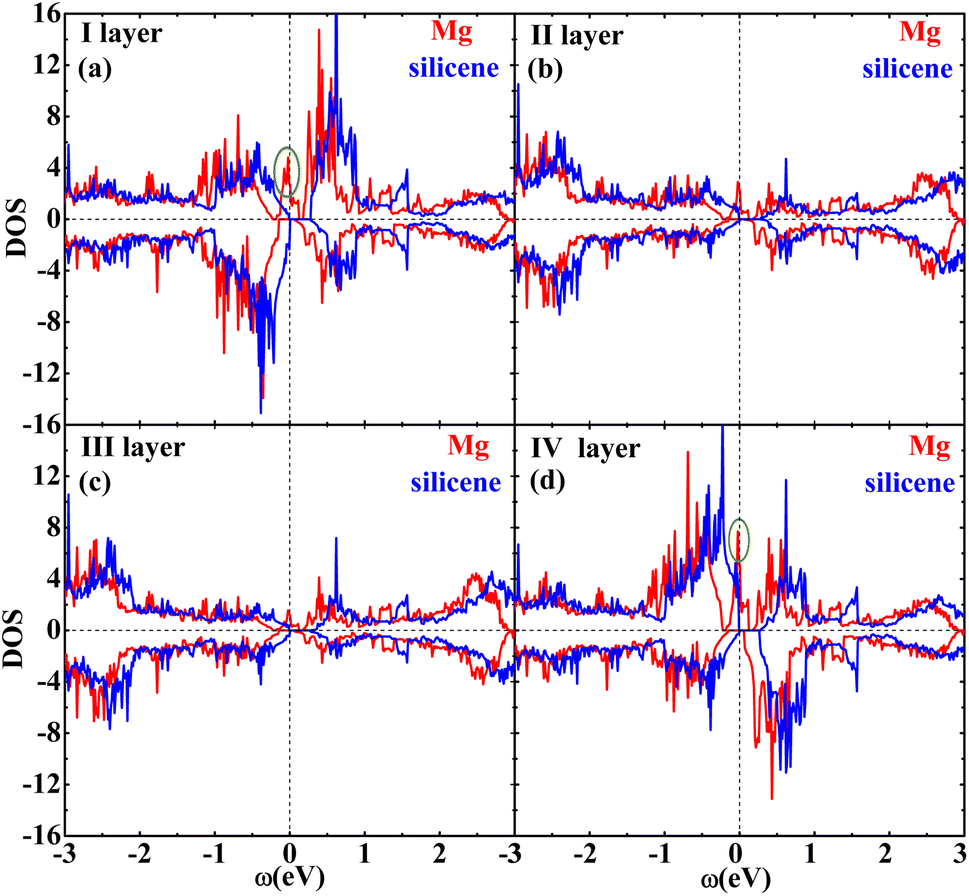 | ||
| Fig. 3 The DOS of the I layer (a), II layer (b), III layer (c) and IV layer (d) of the Mg adsorption system (red) as well as silicene (blue). | ||
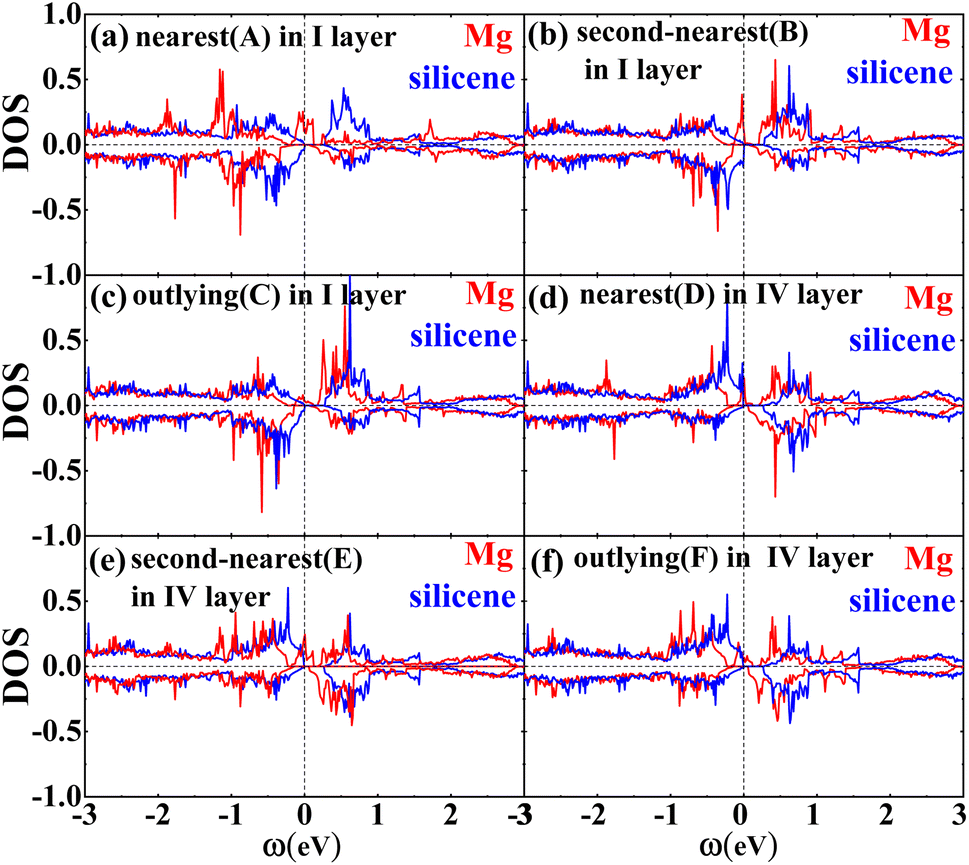 | ||
| Fig. 4 (a), (b) and (c) show the average DOS of the nearest Si (marked with A), next-nearest Si (marked with B) and outlying Si (marked with C) in the I layer, respectively. (d), (e) and (f) show the average DOS of the nearest Si (marked with D), next-nearest Si (marked with E) and outlying Si (marked with F), respectively. The silicene and Mg-adsorbed systems are represented by blue and red, respectively. | ||
To understand the reason why the half-metallicity is induced by non-magnetic atoms, we calculated the magnetic moment of the Si atoms of adsorbed systems as well as pristine silicene. Table 1 shows that the magnetic moment of Si in the I layer for pristine silicene has a value of −0.094 μB. After adsorbing non-magnetic atoms, the magnetic moment of the nearest Si (μA (μB)) decreases or even flips, inducing net spin up magnetic moment, as shown in Table 1. Especially for the alkaline-earth atoms, B and Al, this trend is more obvious due to more transferred charge. Meanwhile, the magnetic moment of the next-nearest Si in the I layer (μB (μB)) also decreases slightly. But, the change in magnetic moment of other Si atoms is almost negligible. Considering the atomic DOS and magnetic moment of Si atoms, we obtain that the effects of adsorbed atoms on Si atoms are different rather than equivalent.
To investigate the role of charge density on distribution of spin density, we compare the CDD and SDD between the Mg-adsorbed system and silicene, as shown in Fig. 5. Fig. 5(a) and (c) show that the charge transferred from Mg to silicene mainly locates in the nearest and next-nearest Si. As shown in Fig. 5(b) and (d), spin densities of the nearest and next-nearest Si in the I layer change obviously, while has a negligible effect on the outlying Si, which induces different magnetic moments in the Si atoms (μA (μB), μB (μB) and μC (μB)). Therefore, the inhomogeneity of the transferred charge arising from adatoms introduces the required electric field perpendicular to the surface, leading to the split of antiferromagnetic degeneracy and realization of half-metal.
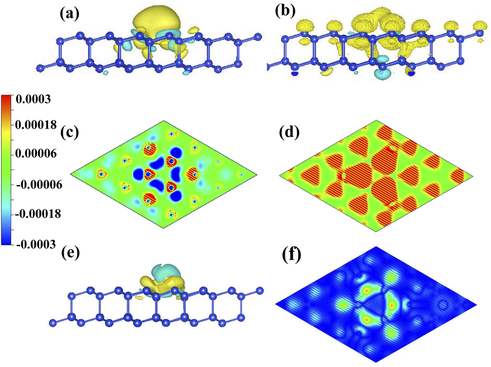 | ||
| Fig. 5 (a) and (b) show the 3D isosurface plots of CDD and SDD (systemMg − silicene). (c) and (d) show projection views of CDD and SDD in the I layer (systemMg − silicene). The 3D isosurface plot of CDD (e) and the projection view of SDD (f) between the Ca-adsorbed and Mg-adsorbed systems (systemCa − systemMg) (the unit is e per Bohr3). | ||
To compare the role of lattice structure and adatoms on the realization of half-metal, the magnetic properties and electronic structures of MgCa and CaMg are calculated in detail. Here, MgCa represents the system in which the Mg atom of the Mg-adsorbed system is replaced with a Ca atom, while CaMg represents the system in which Mg replaces the Ca atom of the Ca-adsorbed system. For the MgCa, the influence of the Ca atom on the nearest Si atom increases, while the effect on the next-nearest Si atom decreases, as shown in row 6 in Table 1. Furthermore, CaMg becomes a half-metal after Mg replaces Ca, as shown in row 8 in Table 1. By comparing Fig. 2(e) and (g), we show that the replacement of the adatom, on the basis of the same structure, changes the band structure significantly, which is also confirmed by comparing Fig. 2(f) and (h). Fig. 2(g) shows a similar band structure as that of Fig. 2(f), although the two systems have different structures. Meanwhile, the electronic structure of siliceneMg is similar to that of pristine silicene, as presented in rows 11 and 12 in Table 1. Here, siliceneMg describes the system in which the Mg atom is directly taken away from the Mg-adsorbed structure. Summarizing the above results, we come to the conclusion that the adatoms play a major role in the realization of the half-metal, while the effect of the lattice structure is almost negligible.
Due to less valence charge than Mg, the silicene absorbed with alkali metal is partially spin-polarized, as shown in Fig. 2(a), (b) and (c). However, the Ca-adsorbed system is a semiconductor in spite of having the same valence charge as that of the Mg atom. To analyze the difference, the CDD and SDD between the Mg-adsorbed and Ca-adsorbed systems are calculated. Fig. 5(e) shows that the influence of charge transfer from the Ca atom on the nearest Si is greater than that of the Mg atom, due to the weaker electronegativity and larger atomic radius of the Ca atom. Therefore, compared with the Mg-adsorbed system, the magnetic moment of the nearest Si in the Ca-adsorbed system changes obviously, as shown in Fig. 5(f). Hence, the distributions of the three bands around the Fermi level (red line surrounded by olive oval, as shown in Fig. 2(e) and (f)) are significantly different.
In order to confirm the generality of the realization of half-metallicity, the electronic structures of Mg-adsorbed systems with various adatomic heights are calculated systematically. The calculated parameters including adatomic height, transferred charge, adsorption energy and magnetic moments are shown in Table 2. It shows that the charge transferred from the adatom to silicene decreases monotonously with the increase in adatomic height, resulting in a weaker effect on the magnetic moment of the nearest Si and next-nearest Si. From Table 2, we also found that the electronic structure is closely dependent on the total magnetic moment and half-metallicity is achieved when the total magnetic moment is greater than 0.6 μB, showing that there is a relatively large range of adsorption concentration to realize half-metallicity. Furthermore, the adsorption energies of the various heights are all negative, confirming that it is feasible to obtain adsorption systems through deposition of non-magnetic atoms experimentally.
| h (Å) | ρad (e) | Eads (eV) | μA (μB) | μB (μB) | μtot (μB) | Eg (eV) |
|---|---|---|---|---|---|---|
| 1.4 | 1.360 | −1.500 | 0.003 | −0.028 | 0.531 | Metal |
| 1.6 | 1.212 | −1.526 | −0.002 | −0.037 | 0.613 | H-metal |
| 1.8 | 1.105 | −1.462 | −0.008 | −0.045 | 0.619 | H-metal |
| 2.0 | 0.983 | −1.318 | −0.008 | −0.048 | 0.601 | H-metal |
To check the stability of the antiferromagnetic bilayer silicene, we performed spin polarized ab initio molecular dynamics (MD) simulations on a 6 × 6 supercell containing 144 Si atoms with a Nosé–Hoover thermostat50 method. Our results clearly indicate that the structure remains unchanged at 100 K, as shown in Fig. 7(a) and (b), in addition to small fluctuations of the temperature and magnetic moment, as displayed in Fig. 6(a) and (b). Based on Fig. 6(c), we could know that the average should be around the desired room temperature, while the antiferromagnetic ground state is not well maintained, as shown in Fig. 6(d). In addition, after 10 ps, we find some structure destruction of the bilayer silicene, as shown in Fig. 7(c) and (d). The transition between 100 K and 300 K indicates the existence of a structural transformation at finite temperature between 100 and 300 K. It indicates that there is a stable structure above liquid nitrogen temperature. Furthermore, we may be able to design antiferromagnetic layered materials stable at room temperature by changing the composition and structure. Therefore, the realization of half-metallicity on the basis of antiferromagnetic two-dimensional materials have wide applications in electronic devices.
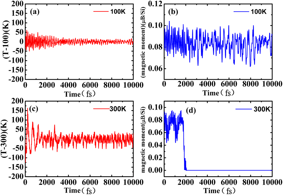 | ||
| Fig. 6 (a) and (b) show the fluctuations of temperature and magnetic moment as a function of time at 100 K. (c) and (d) show the fluctuations of temperature and magnetic moment as a function of time at 300 K for antiferromagnetic bilayer silicene. | ||
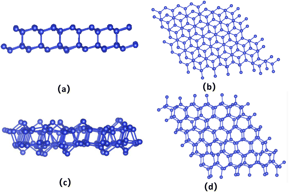 | ||
| Fig. 7 The side view (a) and front view (b) of bilayer silicene after 10 ps of molecular dynamics at 100 K. The side view (c) and front view (d) of bilayer silicene after 10 ps of molecular dynamics at 300 K. | ||
It is well known that the general gradient approximation (Perdew–Burke–Ernzerhof exchange–correlation functional) will significantly underestimate the size of the band gap. A hybrid functional such as HSE06 is expected to perform very well in predicting the accurate band gap and magnetic moment. Fig. 8(b) presents the calculated band structures of PBE and HSE06. It clearly shows that both functionals predicted similar dispersion curves for the valence and conduction bands around the Fermi level, but the position of the conduction bands is significantly up-shifted, resulting in an increase in the band gap of about 1 eV. The band-gap calculated with HSE06 is confirmed to increase by 1 eV in carbon-based materials.51 Remarkably, we found that the ground state still remains antiferromagnetic for HSE06. On the other hand, the van der Waals correction with the D2 functional was not only used to correct the DOS but also to relax the pristine silicene. The results show that the van der Waals correction with the D2 functional hardly changes the band structures, as shown in Fig. 8(a). Hence, the predicted antiferromagnetism and half-metallicity do not depend on the exchange–correlation functional.
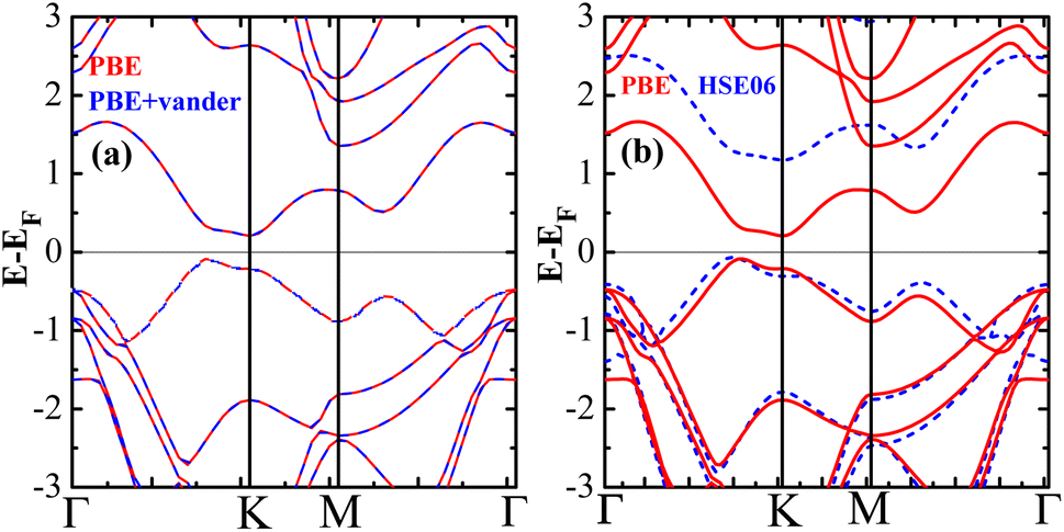 | ||
| Fig. 8 (a) Band structures of PBE with van der Waals correction, (b) band structures calculated by HSE06 and PBE, respectively, for antiferromagnetic bilayer silicene. | ||
In this paper, half-metallicity is realized on bilayer silicene by adsorbing non-magnetic atoms due to the inhomogeneity of the transferred charge. The realization of half-metallicity has also been proved theoretically by inhomogeneous strain through the out-of-plane bending on bilayer silicene.47 Although the above methods of obtaining half-metals are different, both are based on bilayer antiferromagnetic materials. So, the half-metal may be obtained by deposition of non-magnetic atoms as long as the material is a van der Waals layered two-dimensional material with an interlayer antiferromagnetic state. Compared with other complicated requirements such as nanoribbon defects, transition-metal magnetic atoms, magnetic field, semihydrogenation and nitrogenation, this method is more advantageous in practical operation and zero-macroscopic ferromagnetism. Moreover, several studies have confirmed that the slightly bulked bilayer silicene has an antiferromagnetic ground state due to the breaking of the original π-bonding attributed to strong covalent interlayer bonding,48,52 which indicates that other bilayer materials with slightly bulked structures may have an interlayer antiferromagnetic ground state. Therefore, deposition of non-magnetic atoms to realize half-metallicity may not only be suitable for bilayer silicene, but also suitable for other bilayer materials. Our work may provide a feasible route to overcome the major challenge of spintronics.
IV. Conclusions
In conclusion, we predict a bilayer silicene with an interlayer antiferromagnetic ground state, which will become an ideal half-metal by adsorbing non-magnetic atoms. The localization of charge transfer from the adatoms to silicene results in the split of antiferromagnetic degeneracy and realization of half-metal. Therefore, we propose a new mechanism to realize half-metals by depositing non-magnetic atoms in two-dimensional layered materials with interlayer antiferromagnetic states in the absence of a ferromagnetic substrate/magnetic ions/magnetic field, strong in-plane electric field or nanoribbons. Our findings may provide a more feasible way for the development of spintronic devices.Conflicts of interest
There are no conflicts to declare.Acknowledgements
This work is supported by the National Natural Science Foundation of China (No. 11774258, 11174219) and Key Scientific Research Projects of Colleges and Universities in Henan Province (Grant No. 21A140022).References
- S. A. Wolf, D. D. Awschalom, R. A. Buhrman, J. M. Daughton, S. V. Molnar, M. L. Roukes, A. Y. Chtchelkanova and D. M. Treger, Science, 2001, 294, 1488–1495 CrossRef CAS PubMed
.
- M. Xu, T. Liang, M. Shi and H. Chen, Chem. Rev., 2013, 113, 3766–3798 CrossRef CAS PubMed
- Q. H. Wang, K. K. Zadeh, A. Kis, J. N. Coleman and M. S. Strano, Nat. Nanotechnol., 2012, 7, 699–712 CrossRef CAS PubMed
- A. H. Castro Neto, F. Guinea, N. M. R. Peres, K. S. Novoselov and A. K. Geim, Rev. Mod. Phys., 2009, 81, 109–162 CrossRef CAS
- M. A. H. Vozmediano, M. P. Lopez-Sancho, T. Stauber and F. Guinea, Phys. Rev. B, 2005, 72, 155121–155125 CrossRef
- H. X. Luan, C. W. Zhang, S. S. Li, R. W. Zhang and P. J. Wang, RSC Adv., 2013, 3, 26261–26266 RSC
- Z. Li, W. Xie, X. Liu and Y. Wu, J. Appl. Phys., 2015, 117, 084311–084316 CrossRef
- P. Blonski, J. Tucek, Z. Sofer, V. Mazánek, M. Petr, M. Pumera, M. Otyepka and R. Zboril, J. Am. Chem. Soc., 2017, 139, 3171–3180 CrossRef CAS PubMed
- X. Zhang, Z. Bao, X. Ye, W. Xu, Q. Wang and Y. Liu, Nanoscale, 2017, 9, 11231–11238 RSC
- D. J. Adams, O. Gröning, C. A. Pignedoli, P. Ruffieux, R. Fasel and D. Passerone, Phys. Rev. B: Condens. Matter Mater. Phys., 2012, 85, 245405–245409 CrossRef
- Y. Yao, E. Ashalley, X. Niu, L. Dai, P. Yu, W. Chen, Z. Qin, L. Zhang and Z. Wang, Appl. Phys. Lett., 2019, 114, 073101–073104 CrossRef
- E. Şaşıoğlu, H. Hadipour, C. Friedrich, S. Blügel and I. Mertig, Phys. Rev. B, 2017, 95, 060408–060412 CrossRef
- E. Torun, H. Sahin, S. K. Singh and F. M. Peeters, Appl. Phys. Lett., 2015, 106, 192404–192407 CrossRef
- C. Si, J. Zhou and Z. Sun, ACS Appl. Mater. Interfaces, 2015, 7, 17510–17515 CrossRef CAS PubMed
- J. Hea and S. Li, Comput. Mater. Sci., 2018, 152, 151–157 CrossRef
- C. Gong, L. Li, Z. Li, H. Ji, A. Stern, Y. Xia, T. Cao, W. Bao, C. Wang, Y. Wang, Z. Q. Qiu, R. J. Cava, S. G. Louie, J. Xia and X. Zhang, Nature, 2017, 546, 265–281 CrossRef CAS PubMed
- Z. Fei, B. Huang, P. Malinowski, W. Wang, T. Song, J. Sanchez, W. Yao, D. Xiao, X. Zhu, A. F. May, W. Wu, D. H. Cobden, J. Chu and X. Xu, Nat. Mater., 2018, 17, 778–783 CrossRef CAS PubMed
- B. Huang, G. Clark, E. N. Moratalla, D. R. Klein, R. Cheng, K. L. Seyler, D. Zhong, E. Schmidgall, M. A. McGuire, D. H. Cobden, W. Yao, D. Xiao, P. J. Herrero and X. Xu, Nature, 2017, 546, 270–284 CrossRef CAS PubMed
- B. Zhang, G. Song, J. Sun, J. Leng, C. Zhang and J. Wang, Nanoscale, 2020, 12, 12490–12496 RSC
- D. Zhang, A. Rahman, W. Qin, X. Li, P. Cui and Z. Zhang, Phys. Rev. B, 2020, 101, 205119–205125 CrossRef CAS
- H. Ishizuka and Y. Motome, Phys. Rev. Lett., 2012, 109, 237207–237211 CrossRef PubMed
- A. Du, S. Sanvito and S. C. Smith, Phys. Rev. B: Condens. Matter Mater. Phys., 2012, 108, 197207–197211 Search PubMed
- Z. Liu, J. Liu and J. Zhao, Nano Res., 2017, 10, 1972–1979 CrossRef CAS
- X. Zhang, A. Wang and M. Zhao, Carbon, 2015, 84, 1–8 CrossRef CAS
- A. Bafekry, M. Faraji, N. N. Hieu, Y. S. Ang, S. Karbasizadeh, I. A. Sarsari and M. Ghergherehchi, Nanotechnology, 2022, 33, 075707–075714 CrossRef CAS PubMed
- J. J. Zhao, H. S. Liu, Z. M. Yu, R. Quhe, S. Zhou, X. Y. Wang, C. C. Liu, H. X. Zhong, N. N. Han, J. Lu, Y. G. Yao and K. Wu, Prog. Mater. Sci., 2016, 83, 24–151 CrossRef CAS
- B. Huang, D. Monsma and I. Appelbaum, Phys. Rev. Lett., 2007, 99, 177209–177212 CrossRef PubMed
- I. Appelbaum, B. Huang and D. Monsma, Nature, 2007, 447, 295–298 CrossRef CAS PubMed
- F. Zheng, C. Zhang, P. Wang and S. Li, J. Appl. Phys., 2013, 113, 154302–154306 CrossRef
- D. Q. Fang, S. Zhang and H. Xu, RSC Adv., 2013, 3, 24075–24080 RSC
- K. Zberecki, R. Swirkowicz and J. Barná, Phys. Rev. B: Condens. Matter Mater. Phys., 2014, 89, 165419–165431 CrossRef
- Z. Wang, J. Jin, M. Sun and X. Dai, J. Supercond. Novel Magn., 2017, 30, 3225–3229 CrossRef CAS
- D. Zhang, M. Long, F. Xie, J. Ouyang, H. Xu and Y. Gao, Sci. Rep., 2016, 6, 23677–23683 CrossRef CAS PubMed
- Y. Wang, J. Zheng, Z. Ni, R. Fei, Q. Liu, R. Quhe, C. Xu, J. Zhou, Z. Gao and J. Lu, Nano, 2012, 7, 1250037–1250045 CrossRef
- F. Pan, R. Quhe, Q. Ge, J. Zheng, Z. Ni, Y. Wang, Z. Gao, L. Wang and J. Lu, Phys. E, 2014, 56, 43–47 CrossRef CAS
- X. F. Yang, Y. S. Liu, J. F. Feng, X. F. Wang, C. W. Zhang and F. Chi, J. Appl. Phys., 2014, 116, 124312–124320 CrossRef
- H. Sahin and F. M. Peeters, Phys. Rev. B: Condens. Matter Mater. Phys., 2013, 87, 085423–085431 CrossRef
- Y. Nie and X. Hu, Phys. Rev. Lett., 2008, 100, 117203–117206 CrossRef PubMed
- Y. Qian, H. Wu, E. Kan, R. Lu and K. Deng, J. Appl. Phys., 2016, 120, 234303–234310 CrossRef
- X. Hu, Adv. Mater., 2012, 24, 294–298 CrossRef CAS PubMed
- X. F. Ouyang, Z. Y. Song and Y. Z. Zhang, Phys. Rev. B, 2018, 98, 075435–075440 CrossRef
- P. E. Blöchl, Phys. Rev. B: Condens. Matter Mater. Phys., 1994, 50, 17953–17978 CrossRef PubMed
- G. Kresse and J. Furthmüller, Phys. Rev. B: Condens. Matter Mater. Phys., 1996, 54, 11169–11186 CrossRef CAS PubMed
- G. Kresse and J. Furthmüller, Comput. Mater. Sci., 1996, 6, 15–50 CrossRef CAS
- J. P. Perdew, K. Burke and M. Ernzerhof, Phys. Rev. Lett., 1996, 77, 3865–3868 CrossRef CAS PubMed
- T. H. Gao, Acta Phys. Sin., 2015, 64, 076801–076808 CrossRef
- J. L. Shi, Y. H. Wang, X. J. Zhao, Y. Z. Zhang, S. J. Yuan, S. H. Wei and D. B. Zhang, Phys. Chem. Chem. Phys., 2020, 22, 11567–11571 RSC
- X. Wang and Z. Wu, Phys. Chem. Chem. Phys., 2017, 19, 2148–2154 RSC
- K. T. Chan, J. B. Neaton and M. L. Cohen, Phys. Rev. B: Condens. Matter Mater. Phys., 2008, 77, 235430–235441 CrossRef
- D. J. Evans and B. L. Holian, J. Chem. Phys., 1985, 83, 4069–4075 CrossRef CAS
- A. J. Du, Z. H. Zhu and S. C. Smith, J. Am. Chem. Soc., 2010, 132, 2876–2877 CrossRef CAS PubMed
- F. Liu, C. Liu, K. Wu, F. Yang and Y. Yao, Phys. Rev. Lett., 2013, 111, 066804–066808 CrossRef PubMed
| This journal is © The Royal Society of Chemistry 2023 |