
 Open Access Article
 This Open Access Article is licensed under a Creative Commons Attribution-Non Commercial 3.0 Unported Licence
High-performance diodes based on black phosphorus/carbon nanomaterial heterostructures
Xiaowo
Ye†
 ,
Yanming
Zhang†
,
Shengguang
Gao
,
Xiuzhi
Zhao
,
Ke
Xu
,
Long
Wang
,
Shenghao
Jiang
,
Fangyuan
Shi
,
Jingyun
Yang
,
Zhe
Cao
and
Changxin
Chen
*
,
Yanming
Zhang†
,
Shengguang
Gao
,
Xiuzhi
Zhao
,
Ke
Xu
,
Long
Wang
,
Shenghao
Jiang
,
Fangyuan
Shi
,
Jingyun
Yang
,
Zhe
Cao
and
Changxin
Chen
*
National Key Laboratory of Science and Technology on Micro/Nano Fabrication, Key Laboratory for Thin Film and Microfabrication of Ministry of Education, Department of Micro/Nano Electronics, School of Electronic Information and Electrical Engineering, Shanghai Jiao Tong University, Shanghai 200240, China. E-mail: chen.c.x@sjtu.edu.cn
First published on 13th March 2023
Abstract
The performance of diodes, which are the basic building blocks in integrated circuits, highly depends on the materials used. Black phosphorus (BP) and carbon nanomaterials with unique structures and excellent properties can form heterostructures with favorable band matching to fully utilize their respective advantages and thus achieve high diode performance. Here, high-performance Schottky junction diodes based on a two-dimensional (2D) BP/single-walled carbon nanotube (SWCNT) film heterostructure and a BP nanoribbon (PNR) film/graphene heterostructure were investigated for the first time. The fabricated Schottky diode based on the heterostructure with the 10 nm-thick 2D BP stacked on the SWCNT film had a rectification ratio of 2978 and a low ideal factor of 1.5. The Schottky diode based on the heterostructure with the PNR film stacked on the graphene exhibited a high rectification ratio of 4455 and an ideal factor of 1.9. The high rectification ratios for both devices were attributed to the large Schottky barriers formed between the BP and carbon materials, thus leading to a small reverse current. We found that the thickness of the 2D BP in the 2D BP/SWCNT film Schottky diode and the stacking order of the heterostructure in the PNR film/graphene Schottky diode had a significant effect on the rectification ratio. Furthermore, the rectification ratio and breakdown voltage of the resulting PNR film/graphene Schottky diode were larger than those of the 2D BP/SWCNT film Schottky diode, which was attributed to the larger bandgap of the PNRs compared to the 2D BP. This study demonstrates that high-performance diodes can be achieved via the collaborative application of BP and carbon nanomaterials.
1. Introduction
Diodes are the basic building blocks in integrated circuits,1–3 and their performance strongly depends on the materials used. Black phosphorus (BP) and carbon nanomaterials are ideal candidate materials to construct diodes because of their unique structures and excellent properties. BP has a high theoretical hole mobility of 20![[thin space (1/6-em)]](https://www.rsc.org/images/entities/char_2009.gif) 000 cm2 V−1 s−1, an adjustable direct bandgap, and excellent mechanical properties.1,4–8 Besides the layer number, the width of the BP can also provide an additional dimension to tune the bandgap. The narrow one-dimensional (1D) BP nanoribbons (PNRs) can present a larger bandgap than the two-dimensional (2D) BP with similar thickness due to strong quantum confinement effects in width as well as marked edge effects.9,10 These features overcome the challenge of thin large-area 2D BP. In addition, single-walled carbon nanotubes (SWCNT) and graphene have high carrier mobility (>100000 cm−2 V−1 s−1) and conductivity (106 S m−1). They also have fully saturated surface bonds and no interface states.11–18 If these materials can be used to collaboratively construct diodes, then their respective advantages can be fully utilized to achieve high device performance.
000 cm2 V−1 s−1, an adjustable direct bandgap, and excellent mechanical properties.1,4–8 Besides the layer number, the width of the BP can also provide an additional dimension to tune the bandgap. The narrow one-dimensional (1D) BP nanoribbons (PNRs) can present a larger bandgap than the two-dimensional (2D) BP with similar thickness due to strong quantum confinement effects in width as well as marked edge effects.9,10 These features overcome the challenge of thin large-area 2D BP. In addition, single-walled carbon nanotubes (SWCNT) and graphene have high carrier mobility (>100000 cm−2 V−1 s−1) and conductivity (106 S m−1). They also have fully saturated surface bonds and no interface states.11–18 If these materials can be used to collaboratively construct diodes, then their respective advantages can be fully utilized to achieve high device performance.
Diversified junctions have been used to form built-in electric fields for fabricating diodes based on the BP or carbon materials including p–n junction, heterojunction, and Schottky junction.5,8,13,17–21 We previously investigated a p–i–n junction diode based on locally-doped individual SWCNTs or an SWCNT network. This led to a rectification ratio of 104 and an ideal factor of 1.3.13,17,18 A diode based on the gate-controlled BP/WSe2 vertical heterojunction showed an ideal factor of 1.47. However, this diode had a low rectification ratio of 500 and a high series resistance of 5 MΩ.19 An Au/BP/Al Schottky junction diode with asymmetric metal contacts has also been reported and showed a maximum rectification ratio of 1500 under a specific gate-tuning voltage.5 A theoretical study has shown that the BP/CNT heterostructure can form favorable band matching and interface coupling as well as bandgap size. The contact type of this heterostructure can also be tuned via the sizes of the BP or CNT.22 Thus, we expect that using BP and carbon nanomaterials can lead to heterostructures with favorable band matching and a strong built-in electric field for high diode performance.
Here, high-performance Schottky junction diodes based on the 2D BP/SWCNT film heterostructure and the PNR film/graphene. The 2D heterostructure were investigated for the first time. BP was prepared via mechanical exfoliation, and the PNRs with widths ranging from several nanometers to hundreds of nanometers were prepared via liquid phase exfoliation. The resulting 2D BP/SWCNT film Schottky diode had a rectification ratio of 2978 and a low ideal factor of 1.5. The PNR film/graphene Schottky diode exhibited a high rectification ratio of 4455 and an ideal factor of 1.9. The research showed that the thickness of the 2D BP in the 2D BP/SWCNT film Schottky diode and the stacking order of the heterostructure in the PNR film/graphene diode each had a significant effect on the rectification ratio.
2. Results and discussion
In the experiment, the bulk BP crystals were prepared via a short transport reaction. The red phosphorus, Sn, and SnI4 were sealed in a quartz ampoule under a vacuum. Sn and SnI4 were used as the mineralizers, and red phosphorus was the phosphorus source. The ampoules were placed horizontally in a muffle furnace to keep a temperature difference between the two ends of the ampoule. Then, the furnace was heated to 650 °C and held there for 30 min. The furnace was then rapidly cooled over 10 °C within several minutes and kept at 640 °C for 30 min. A similar method was used to cool the furnace at a step length of 10 °C until the temperature reached 450 °C. Finally, the furnace was naturally cooled to room temperature. More details are seen in the Experimental methods.The BP crystal prepared via this method had a metallic luster, smooth surface, and bunch-like shape. The BP bunches were composed of BP crystal branches (Fig. 1a). These branches were 50 μm to 9 mm in width, 3 mm to 18 mm in length, and several micrometers to tens of micrometers thick (Fig. 1b). The BP crystal branches grew from a crystal nucleus and had smooth and tidy edges. The X-ray diffraction (XRD) spectrum of the BP crystal shows three distinct characteristic peaks corresponding to the (020), (040), and (060) planes parallel to the BP layer in the BP single crystal (Fig. 1c).23–25 Except for the typical characteristic peaks of the BP crystal, no other impurity peaks are found in the XRD spectrum, which indicates that the prepared BP has high purity. The BP crystal was also characterized via a transmission electron microscope (TEM). The TEM results showed that the BP crystals have a layered structure without obvious defects (Fig. 1d). Using the tape-assisted mechanical exfoliation method,5 the bulk BP could be exfoliated into 2D BP flakes with a thickness of hundreds of nanometers to several micrometers (Fig. 1e). This in turn could be pressed onto the PDMS or SiO2/Si substrate for later usage.
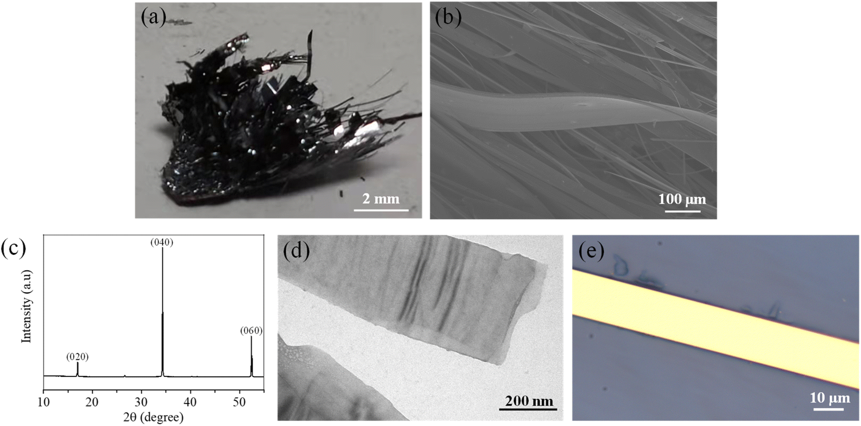 | ||
| Fig. 1 Images and XRD spectrum of the bulk BP crystals. (a) and (b) Optical image (a) and SEM image (b) of the bulk BP bunch. (c) XRD spectrum of a BP crystal branch showing three distinct characteristic peaks corresponding to the (020), (040), and (060) planes parallel to the BP layer in the BP single crystal. (d) TEM image of a BP crystal obtained by the mechanical exfoliation. (e) Optical photograph of a 2D BP flake obtained by the mechanical exfoliation. | ||
We used a liquid phase exfoliation method to prepare the PNR solution. The bulk BP crystals were sonicated in anhydrous dimethyl sulfoxide (DMSO) at a power of 50 W for 6 h to prepare the dispersions and then centrifuged at 14000 rpm for 1 h. The resulting supernatant after the centrifugation was collected. Then, the prepared dispersions were dropped on the silicon dioxide (SiO2)/silicon (Si) substrates and dried in a vacuum. The details can be seen in the Experimental methods. It was observed that the products prepared by the liquid phase exfoliation were mainly composed of 1D PNRs with a small proportion of 2D BP sheets (Fig. 2a). The prepared 1D PNRs had a large aspect ratio. They had a width of several nanometers to hundreds of nanometers, a thickness of about one nanometer to tens of nanometers, and a median length of several micrometers. Fig. 2b shows a PNR with a uniform width of 120 nm. Fig. 2c shows a PNR with a width of 70 nm and a thickness of 18 nm. Atomic force microscope (AFM) and scanning electron microscope (SEM) images showed that the exfoliated PNRs had smooth edges. The SEM image of a typical 2D BP sheet in the product is also shown in Fig. 2d. The side lengths of the exfoliated 2D BP sheets ranged from several micrometers to hundreds of micrometers.
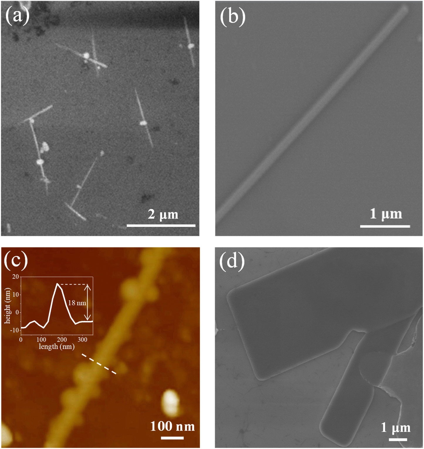 | ||
| Fig. 2 Morphological characterization of the products prepared via liquid phase exfoliation of the bulk BP crystals. (a) SEM image of prepared PNRs. (b) Zoomed-in SEM image of an individual PNR. (c) AFM image of an individual PNR. Inset: the height profile of the PNR measured along the white dashed line perpendicular to the length of the PNR. (d) SEM image of a prepared 2D BP. | ||
The SWCNT films were prepared via the vacuum filtration of the SWCNT solution. Here, SWCNTs were dispersed in an isopropyl alcohol (IPA) solution by ultrasonic treatment, and the solution was then filtered on a polycarbonate (PC) filter membrane with a diameter of 47 mm in a vacuum to obtain a uniform SWCNT film (Fig. 3a). Controlling the concentration and volume of the SWCNT dispersion, we could well control the thickness of the SWCNT film as well as the SWCNT quantity during the fabrication (see the Experimental methods for the details). The SWCNT film was split into small pieces (8 × 8 mm) for device fabrication. The SWCNT film was then transferred to the Si substrate via a wet transfer method showing the disordered network structure under SEM observation (Fig. 3b). The edge of the prepared SWCNT film was straight (Fig. 3c). The SWCNT was also characterized by Raman spectroscopy. Here, the D band and G band of the SWCNT film can be observed at 1360 cm−1 and 1593 cm−1, respectively (Fig. 3d), showing a small D/G intensity ratio. The small D/G intensity ratio indicates that the SWCNTs had few defects, and the sharp G peak indicates the high graphitization degree of the SWCNTs.
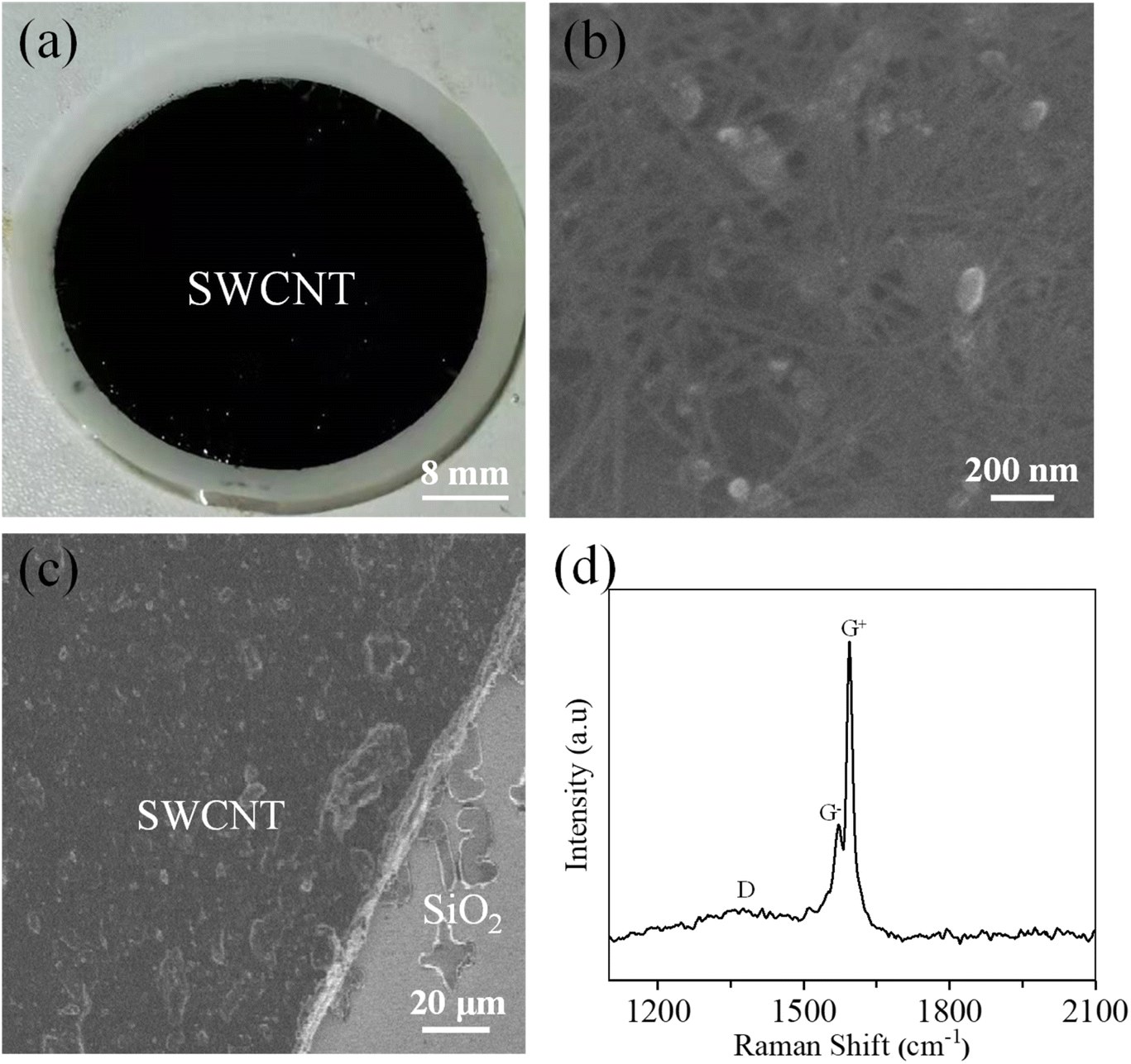 | ||
| Fig. 3 Images and Raman spectrum of the prepared SWCNT film. (a) Optical image of the SWCNT film on the filter membrane. (b) SEM image of the SWCNT film on the SiO2/Si substrate. (c) SEM image of the split SWCNT film with well-defined edges. (d) Raman spectrum of the SWCNT film showing the D band and G band of SWCNTs. | ||
The 2D BP/SWCNT film Schottky diodes were fabricated by stacking the mechanically exfoliated 2D BP flake onto the SWCNT film to form the vertical heterostructure (Fig. 4a and b). A SWCNT film prepared by the vacuum filtration was split into small pieces with a size of 8 × 8 mm and transferred from the filter membrane onto the Si substrate with 100 nm-thick thermally oxidized SiO2. A 2D BP flake with a size of hundreds of micrometers prepared by the tape-assisted mechanical exfoliation method was pressed onto a polydimethylsiloxane (PDMS) substrate. By controlling the times of the tape-assisted exfoliation, we could adjust the thickness of the resulting 2D BP. Using an alignment-transferring platform, we could stack the 2D BP on the SWCNT film precisely to form a 2D BP/SWCNT film vertical heterostructure and control their overlapping area via the dry transfer method. The overlap area between the 2D BP and the SWCNT film was about 1200 μm long and 400 μm wide (Fig. 4c). The silver (Ag) electrodes were fabricated on the 2D BP flake and the SWCNT film. These served as positive and negative electrodes, respectively. The Si substrate was used as the gate of the device, while the SiO2 layer was used as the gate insulator of the device. More fabrication details can be seen in the Experimental methods.
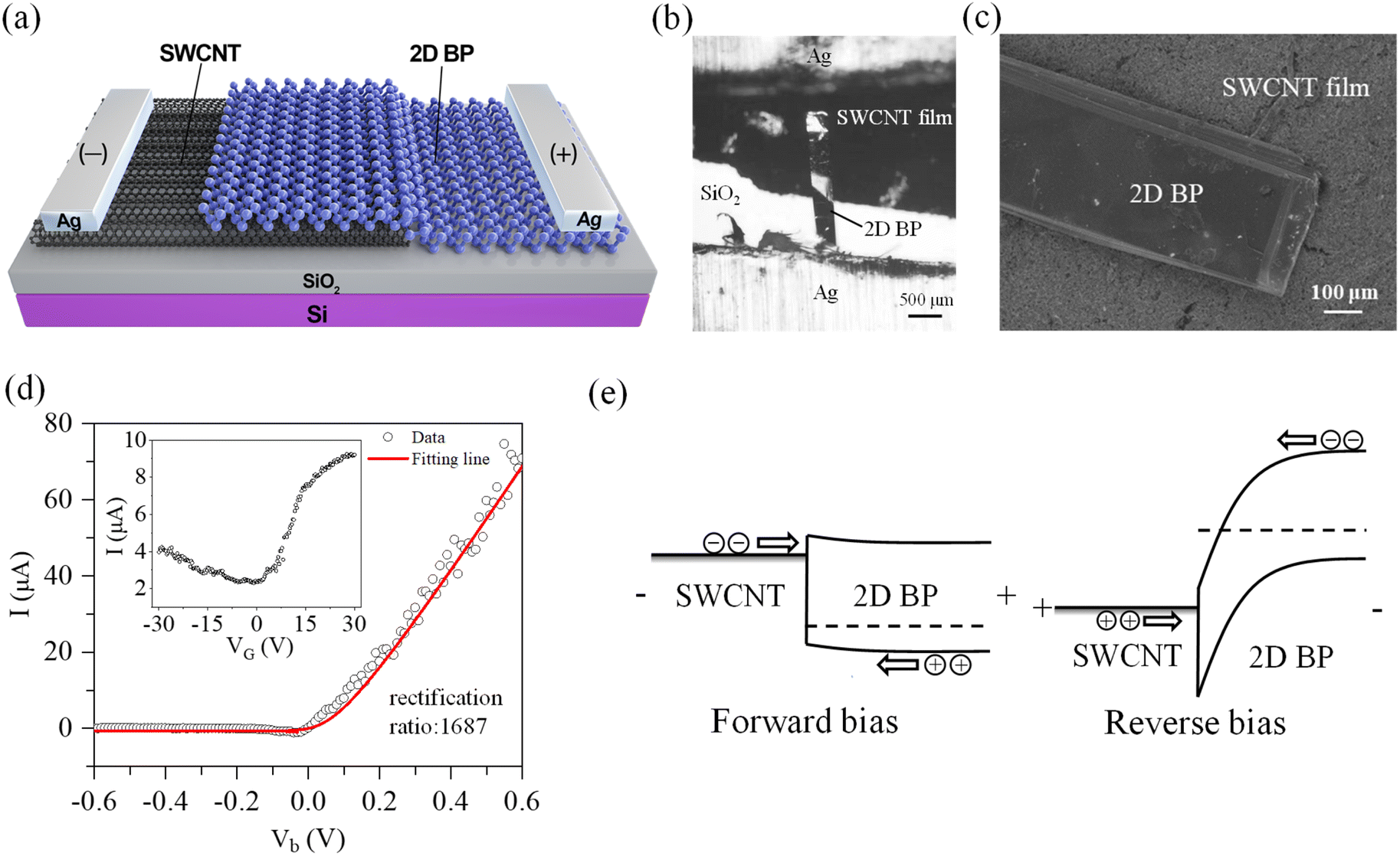 | ||
| Fig. 4 Measurements and operation mechanism of the 2D BP/SWCNT film Schottky diode. (a) Structural schematic of the device. (b) Optical image of the device. (c) Zoomed-in SEM image of the 2D BP/SWCNT film vertical heterostructure. (d) I–V characteristic curve of the diode, showing that the rectification ratio at Vb = ±0.58 V is 1687 and I0 is 115 nA. A red fitting line was obtained via fitting the experimental data using the diode formula with n = 1.1 and Rs = 6.8 kΩ. Inset: the device current as a function of the VG at Vb = 20 mV. (e) Energy band diagrams of the device under the forward bias (left) and the reverse bias (right). | ||
The I–V characteristics of a typical 2D BP/SWCNT film Schottky diode are shown in Fig. 4d. The device current increased rapidly as increasing voltage under forward bias and it tended to be saturated as decreasing voltage under reverse bias, thus showing typical rectification characteristics. The rectification ratio of the diode was 1687 at bias voltage (Vb) = ±0.58 V. The device had a small reverse saturation current of 115 nA. The high rectification ratio and small reverse saturation current could be attributed to the fact that large Schottky barriers were formed between BP and carbon materials. The diode showed a low threshold voltage (Vth) of 0.05 V. To obtain more figures of merit about the diode, the I–V characteristic curve of the device was fitted by the following diode formula,13
 | (1) |
| Junction of the device | n | Rectification ratio | I 0 (nA) | V th (V) | Source |
|---|---|---|---|---|---|
| 2D BP/SWCNT film Schottky junction | 1.5 | 2978 | 0.002 | 0.55 | This work |
| PNR film/graphene Schottky junction | 1.9 | 4455 | 0.002 | 0.7 | This work |
| BP p–n junction | 1.06 | 115 | 50 | 0.08 | Ref. 36 |
| 2D BP/2D MoS2 vertical heterojunction | 1.59 | 1200 | 0.1 | 0.4 | Ref. 27 |
| 2D BP/2D MoS2 vertical heterojunction | 2 | 1500 | 50 | 0.75 | Ref. 28 |
| 2D BP/GaAs vertical heterojunction | 2 | 1000 | 10 | 0.3 | Ref. 29 |
| 2D BP/2D InGaAs vertical heterojunction | 1.6 | 4600 | 0.2 | 0.15 | Ref. 30 |
| 2D BP/2D InSe vertical heterojunction | — | 180 | 0.15 | 0.25 | Ref. 33 |
| 2D BP/graphene vertical heterojunction | 1.5 | 100 | — | 0.1 | Ref. 31 |
| 2D BP/zinc oxide nanowire vertical heterojunction | 1.3 | 10000 |
1 | 0.1 | Ref. 32 |
| Pd/CNT/Al Schottky junction | — | 1012 | 0.01 | 0.2 | Ref. 17 |
| Graphene/Si vertical heterojunction | 2.5 | 100 | 1000 | 0.05 | Ref. 37 |
The rectification behaviors of the 2D BP/SWCNT film diode can be explained by the energy band diagram. Under forward bias, the hole and electron transport currents are both large because there is no Schottky barrier for the hole transport and the Schottky barrier for the electron transport is also small (Fig. 4e, left). Under reverse bias (Fig. 4e, right), the hole and electron transport currents are both small because the Schottky barrier for hole transport is large and the electrons transport as the minority carriers.
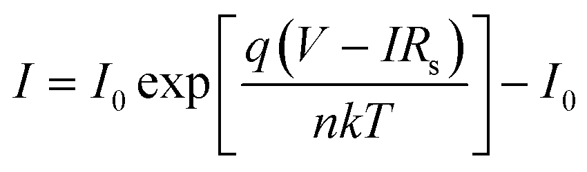
To study the effect of the 2D-BP thickness, we also used a thinner 2D BP of 10 nm to form the heterostructure with a SWCNT film to fabricate the device. The fabrication details are provided in the Experimental methods. Fig. 5a shows an AFM image of the thin layer 2D BP/SWCNT film Schottky diode. Fig. 5b shows a zoomed-in image of the heterostructure of the thin layer 2D BP and the SWCNT film. The thickness of the 2D BP was measured to be 10 nm considering a van der Waals distance of 0.3 nm between the 2D BP and the substrate (inset in Fig. 5b). The thickness of the SWCNT film was also measured to be about 24 nm. The overlap area between the 2D BP and the SWCNT film was about 14 μm2. Fig. 5c shows a zoomed-in AFM image of the SWCNT film. It can be observed that the prepared SWCNT film is very dense. Based on the AFM observation of SWCNTs dispersed on the substrate, we could also judge that most SWCNTs are individual (not bundled) and part of them are bundled. In this device, the electrodes deposited on the 2D BP and the SWCNT film acted as the positive and negative electrodes of the device, respectively. The resulting diode exhibited a rectification ratio of 2978 at Vb = ±1.38 V (Fig. 5d) and an ideal factor of 1.5. The rectification ratio of the thin 2D BP/SWCNT film Schottky diode was larger than that of the thick 2D BP/SWCNT film Schottky diode, which was attributed to the 10 nm-thick 2D BP having a larger bandgap. According to the relationship between the bandgap of the channel material and the Ion/Ioff of the fabricated field-effect transistors (FETs),34 the bandgap of the 2D BP with a thickness of 10 nm can be estimated to be about 0.37 eV from the previous study in ref. 35. The 10 nm-thick 2D BP caused a larger hole Schottky barrier at the contact between it and the SWCNT film compared to the thick 2D BP (Fig. 5e), which led to a smaller reverse saturation current.
 | ||
| Fig. 5 The Schottky diode based on the heterostructure of the thin 2D BP and the SWCNT film. (a) AFM image of the device. (b) Zoomed-in AFM image of the thin 2D BP/SWCNT film heterostructure according to the highlighted region (black square box) in (a). Inset: height profile of the 2D BP, which was measured along the blue dashed line. (c) Zoomed-in AFM image of the SWCNT film according to the highlighted region (white square box) in (a). (d) I–V characteristic curve of the diode. The rectification ratio is 2978 at Vb = ±1.38 V. A red fitting line was obtained via fitting the experimental data using the diode formula. (e) Energy band diagrams of the Schottky contact between thin 2D BP and SWCNT film (left) and the Schottky contact between thick 2D BP and SWCNT film (right) under the reverse bias. | ||
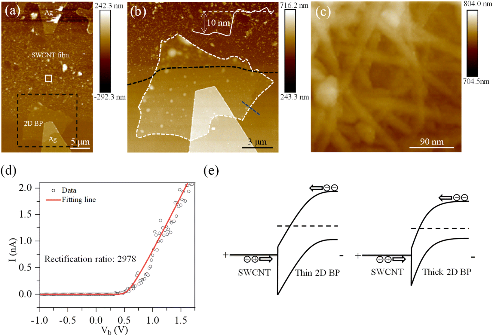
Although the 2D BP could tune the band gap by decreasing the thickness, few-layer large-area BP is difficult to be obtained with current technology. Previously, a theoretical investigation showed that the 1D BP had a larger bandgap compared to its 2D counterpart with similar thickness due to a strong quantum confinement effect in the width direction and the edge effect.10 Based on this consideration, we used the 1D PNR to construct devices with higher rectification ratios. By transferring graphene onto the PNR film to form the PNR film/graphene vertical heterostructure (Fig. 6a), we obtained the PNR film/graphene Schottky diode. The resulting BP dispersions were filtered with a polyvinylidene fluoride (PVDF) filter membrane in vacuum to obtain the PNR film with a thickness of hundreds of nanometers. The PNR film was split into small pieces sized 12 × 2 mm and transferred from the filter membrane onto the small piece of Si wafers with a 100 nm-thick thermally oxidized SiO2 layer. The graphene (5 × 5 mm) was grown by chemical vapor deposition (CVD) and transferred onto the PNR film by the wet transfer method to form favorable contact between them. The overlapping area between the PNR film and the graphene was about 2.4 mm long and 2.0 mm wide (Fig. 6b). The Ag electrodes were fabricated on the PNR film and the graphene. These were used as the positive and negative electrodes, respectively.
 | ||
| Fig. 6 Measurements and operation mechanism of the PNR film/graphene Schottky diode. (a) Structural schematic of the device. (b) Optical image of diode with the graphene stacked on the PNR film. (c) I–V characteristic curve of the diode. The rectification ratio at Vb = ±2.16 V is 3982 and the I0 is 2.5 nA. The red fitting line obtained by fitting the experimental data using the diode formula. (d) Optical image of diode with the PNR film stacked on the graphene. (e) I–V characteristic curve of the diode. The rectification ratio is 4455 at Vb = ±1 V and the I0 is 0.002 nA. The red fitting line obtained by fitting the experimental data using the diode formula. (f) Energy band diagrams of the PNR film/graphene Schottky contact (left) and the 2D BP/SWCNT film Schottky contact (right) under reverse bias. | ||
The resulting PNR film/graphene Schottky diode showed good rectification characteristics (Fig. 6c). The rectification ratio at Vb = ±2.16 V could reach 3982, which is higher than most previously reported BP-based diodes27–29,31,33,36 and graphene-based diodes.37 A detailed comparison between these devices is listed in Table 1. The device had a low reverse saturation current of 2.5 nA and a threshold voltage of 0.6 V. A n value of 2.9 and an Rs of 620 kΩ were obtained by fitting the measured I–V characteristic curve with the formula (1). The n value of the PNR film/graphene Schottky diode was larger than that of the 2D BP/SWCNT film Schottky diode because the defects on the PNR edges cause more carrier recombination in the junction region.6 The diode exhibited a breakdown voltage of −2.7 V.
We also studied the effect of the stacking order of the heterostructure on the device performance. The PNR film/graphene Schottky diode based on the heterostructure with the PNR film stacked on the graphene was fabricated (Fig. 6d). The rectification ratio of this diode reached 4455 at Vb = ±1 V. By fitting the measured I–V characteristic curve with the formula (1), an n value of 1.9 and an Rs of 20 MΩ were obtained (Fig. 6e). The larger rectification ratio obtained by the device when placing the PNR film on the graphene may have been the result of better contact with the PNR film and the graphene.
It was found that the PNR based diodes had a larger rectification ratio and better breakdown voltage than 2D BP based diodes. These findings were explained by the PNRs having a larger bandgap than the 2D BP due to a strong quantum confinement effect in width and the edge effect.10 In turn, there was a higher and thicker hole Schottky barrier at the PNR film/graphene contact (Fig. 6f, left) than at the 2D BP/SWCNT film contact (Fig. 6f, right). This leads to a smaller reverse saturation current, and a larger reverse bias voltage as required for tunneling current of the holes.
3. Conclusions
In this paper, high-performance Schottky diodes based on the 2D BP/SWCNT film heterostructure and the PNR film/graphene heterostructure were investigated. The 2D BP/SWCNT film Schottky diode had a rectification ratio of 2978 and a low ideal factor of 1.5. The PNR film/graphene Schottky diode exhibited a high rectification ratio of 4455 and an ideal factor of 1.9. The high rectification ratios for both devices were caused by the large Schottky barriers formed between BP and carbon materials, thus causing a small reverse current. The research showed that the thin 10 nm-thick 2D BP/SWCNT film Schottky diode had a higher rectification ratio than the thick 2D BP/SWCNT film Schottky diode. The diode with the PNR film stacked on the graphene had a higher rectification ratio than the diode with the graphene placed on the PNR film. It was also shown that the rectification ratio and breakdown voltage of the PNR film/graphene Schottky diode were larger than those of the 2D BP/SWCNT film Schottky diode. This finding can be explained by the used PNRs having a larger bandgap than the 2D BP which results in a larger hole Schottky barrier between the PNRs and graphene under the reverse bias. This work has provided a method to fabricate high-performance diodes based on the collaborative application of BP and carbon nanomaterials. This kind of diode can also be applied as photovoltaic devices or photodetectors.4. Experimental methods
4.1 Growth of the bulk BP crystals
High-quality bulk BP crystals were prepared via a short transport reaction. 0.5 g red phosphorus, 20 mg Sn, and 10 mg SnI4 were sealed in a quartz ampoule with an inner diameter of 8 mm at 0.1 Pa. The Sn and SnI4 were used as the mineralizers, and the red phosphorus was the phosphorus source. The ampoules were placed horizontally in a muffle furnace with one end close to the furnace wall and the heating resistance wire; the other end was close to the middle of the furnace. The sample was placed on the end of the ampoule close to the furnace wall. Then, the furnace was heated to 650 °C and kept at this temperature for 30 min. The furnace was then rapidly cooled down to 640 °C within several minutes and kept at this temperature until the total time reached 30 min. We similarly cooled the furnace at a step length of 10 °C until the temperature of the furnace reached 450 °C. Finally, the furnace was naturally cooled to room temperature.4.2 TEM characterizations of the 2D BP
The samples were prepared by dropping diluted BP solutions onto TEM grids, which were laid on a piece of filter paper. The TEM grids were lacey carbon-coated 200 mesh gold grids (SPI Supplies). The resulting TEM grids were dipped and rinsed in dichloroethane for 10 min. The TEM observation and imaging of the samples were performed on a thermofisher TALOS F200X instrument.4.3 Preparation of the PNR films on the SiO2/Si substrates
Here, 30 mg bulk BP crystals were added into 300 ml DMSO. The solution was treated with ultrasonication at 50 W for 6 h to prepare the PNR dispersions. During the ultrasonication treatment, the solution was kept in the nitrogen (N2) atmosphere at 25 °C. The resulting PNR dispersions were centrifuged at 14000 rpm for 1 h. Eventually, the supernatant of the PNR dispersions was collected after centrifugation. The resulting solution was prepared in the PNR thin film via vacuum filtration using the PVDF filter membrane with a pore size of 0.2 μm. The PNR films were dense and had a uniform thickness of hundreds of nanometers. The resulting filter membrane with the PNR film was split into small pieces with a size of several millimeters. These were placed onto the 2 × 2 cm SiO2/Si substrates with PNR films downward. Moderate pressure was then applied on the filter membrane for 20 min in a vacuum. Finally, the filter membrane was carefully torn off leaving the PNR film on the SiO2/Si substrate surface.
4.4 Preparation of the SWCNT films on SiO2/Si substrates
SWCNTs with an average diameter of 1.4 nm (Model: P3, Carbon Solutions Inc., USA) were used. First, 10 mg SWCNTs were added into 150 ml IPA. The solution was then sonicated at 240 W for 2 h in an ice-water bath to form a uniformly dispersed SWCNT solution. The resulting SWCNT dispersions were used to prepare the SWCNT films by vacuum filtration. The PC filter membrane with a pore size of 0.2 μm was used in this process. After vacuum filtration, SWCNT films with a uniform thickness of tens of nanometers to hundreds of nanometers were obtained. The filter membrane containing the SWCNT film was split into small pieces, which were then suspended on the N-methylpyrrolidone (NMP) solution surface with the SWCNT films upward. Thus, the filter membrane was dissolved in the NMP solution and an SWCNT film floating on the solution surface was obtained. Finally, the SWCNT films were lifted and transferred onto the 2 × 2 cm SiO2/Si wafers.4.5 SEM observation of the bulk BP, PNRs, and SWCNT films
The bulk BP, PNRs, and SWCNT films were observed by SEM (Sigma 500 scanning electron microscope, Zeiss, Germany). The PNR samples for SEM observations were prepared as follows: the PNR solution was dropped on the 1 × 1 cm SiO2/Si wafers. These wafers were heated to 65 °C within 20 min and kept at this temperature for 6 h in a quartz tube furnace at 10−3 Pa. The resulting samples were sequentially rinsed with the DMSO and IPA for a couple of minutes to remove the large BP impurities and then blown dry. The accelerating voltage of the SEM was 5 kV.4.6 XRD characterization of the BP crystals
The XRD characterization of the BP crystals used a multifunctional X-ray powder diffractometer (D8 ADVANCE Da Vinci diffractometer, Bruker, Germany) with Cu Kα radiation and wavelengths of λ1 = 1.54056 Å and λ2 = 1.54439 Å.4.7 AFM characterization of the thin layer 2D BP/SWCNT film Schottky diode and the PNRs
Atomic force microscopy (Dimension Icon & Fast-Scan Bio AFM from Bruker, Germany) was used for observing and measuring the PNR samples. Commercial AFM tips (Olympus Micro Cantilevers Company, Model: OMCL-AC240TS-R3) were used. The AFM tip has a tip radius of 7 nm, a spring constant of 1.7 N m−1, and a resonant frequency of 70 kHz. To obtain a more accurate width, the same AFM tips were used to measure the apparent widths and heights of the CVD-grown multiwalled carbon nanotubes. These have similar heights as the measured PNRs to deduce the effect of the AFM tip size on the PNR width. According to our measurement, the actual width of the PNR was about 14 nm less than the measured apparent width when the effect of the AFM tip size was corrected.4.8 Raman measurements of the SWCNT films
A Raman system (TESCAN RISE-MAGNA, Czech) was used to measure the Raman spectrum of the SWCNT film. A 532 nm laser was used as the excitation light whose spot size was 0.46 μm under 100× objective. A laser power of 0.507 mW, a numerical aperture of 0.75, and an exposure time of 15 s per spot were used in the Raman measurements.4.9 Fabrication of the 2D BP/SWCNT film Schottky diodes
The SWCNT film on the filter membrane was spilt into small pieces with a size of 8 × 8 mm and transferred onto the 2 × 2 cm Si wafers with a 100 nm-thick thermally oxidized SiO2 layer via the above-mentioned wet transfer method. Next, different thicknesses of 2D BP can be obtained by the tape-assisted exfoliation method5 with different exfoliation times. The thick and 10 nm-thick 2D BP were selected for usage. The 2D BP was first pressed onto a PDMS substrate. The 2D BP on the PDMS was then transferred onto the SWCNT film via a dry transfer method in an alignment-transferring platform to form a 2D BP/SWCNT film vertical heterostructure. The overlap region of the 2D BP and the SWCNT film was about 980 μm long and 400 μm wide. The Ag electrodes were fabricated on the 2D BP and the SWCNT film to act as the positive and negative electrodes of the device. A gold film was deposited on the back of the Si wafer by applying the gate voltage to the Si substrate used as the gate electrode. The SiO2 layer in the device was used as the gate insulator.4.10 Fabrication of the PNR film/graphene Schottky diodes
PNR films with a size of 12 × 2 mm were first prepared on the 2 × 2 cm Si substrates with 100 nm-thick thermally oxidized SiO2 layer. Graphene on the copper (Cu) foil grown by the CVD method (Hefei Microcrystalline Material Technology Co., Ltd) was used in the experiment. The polymethyl methacrylate (PMMA) photoresist was spin-coated on the graphene/Cu structure to act as the supporting layer of the graphene. The PMMA/graphene/Cu structure was split into 5 × 5 mm sizes. This then floated on the copper etching solution surface for 3 h to remove the copper substrate. The PMMA/graphene structure was transferred into IPA and floated on its surface for later usage.To fabricate the diodes based on graphene stacking on the PNR film, the prepared graphene was lifted and transferred onto the SiO2/Si substrate with the PNR film to form the PNR film/graphene vertical heterostructure. The overlap region of the PNR film and the graphene was about 2.4 mm long and 2.0 mm wide. The resulting structure was soaked in acetone for 60 min to remove the PMMA and then blown dry by N2. The Ag electrodes were fabricated on the PNR film and the graphene acts as the positive and negative electrodes of the device.
To fabricate the diodes based on PNR film stacking on the graphene, the prepared graphene was transferred onto the SiO2/Si substrate and then the resulting samples were soaked in acetone for 60 min and blown dry by N2. The PNR film was transferred onto the wafer with the graphene to form the vertical heterostructure. The overlap region of the PNR film and the graphene was about 2 mm long and 0.5 mm wide. Finally, the Ag electrodes were fabricated on the PNR film and the graphene acted as the positive and negative electrodes of the device.
4.11 Electrical measurements of the diodes
The electrical characteristics of the 2D BP/SWCNT film Schottky diode and the PNR film/graphene Schottky diode were tested with an Agilent B1500A semiconductor performance analyzer. Here, the bias voltage was applied to the 2D BP or PNR film with the SWCNT film or graphene grounded. The devices were tested in a vacuum with a vacuum degree of 8 × 10⁻⁵ Pa. The device current as a function of the gate voltage was also measured.Author contributions
C. C. conceived and designed the experiments. X. Y., Y. Z., S. G., X. Z., K. X., L. W., S. J., F. S., J. Y. and Z. C. performed the experiments. X. Y., Y. Z., S. G., X. Z., K. X., S. J. and C. C. analysed the data. C. C., X. Y. and Y. Z. wrote the manuscript. All the authors discussed the results and commented on the manuscript. C. C. planned and supervised the project.Conflicts of interest
There are no conflicts to declare.Acknowledgements
This work was supported by the National Natural Science Foundation of China for Excellent Young Scholars (No. 61622404), National Natural Science Foundation of China (No. 62074098), Chang Jiang (Cheung Kong) Scholars Program of Ministry of Education of China (No. Q2017081) and Project from Zhejiang Fulai New Material Company. The authors thank the Center for Advanced Electronic Materials and Devices (AEMD) at Shanghai Jiao Tong University for the support of device processes.References
- Y. Liu, Y. Cai, G. Zhang, Y. W. Zhang and K. W. Ang, Al-doped black phosphorus p–n homojunction diode for high performance photovoltaic, Adv. Funct. Mater., 2017, 27(7), 1604638 CrossRef.
- D. Jariwala, V. K. Sangwan, C. C. Wu, P. L. Prabhumirashi, M. L. Geier, T. J. Marks, L. J. Lauhon and M. C. Hersam, Gate-tunable carbon nanotube–MoS2 heterojunction pn diode, Proc. Natl. Acad. Sci. U. S. A., 2013, 110(45), 18076–18080 CrossRef CAS PubMed.
- W. Xin, X. K. Li, X. L. He, B. W. Su, X. Q. Jiang, K. X. Huang, X. F. Zhou, Z. B. Liu and J. G. Tian, Black-phosphorus-based orientation-induced diodes, Adv. Mater., 2018, 30(2), 1704653 CrossRef PubMed.
- J. Qiao, X. Kong, Z. X. Hu, F. Yang and W. Ji, High-mobility transport anisotropy and linear dichroism in few-layer black phosphorus, Nat. Commun., 2014, 5(1), 1–7 Search PubMed.
- J. Miao, S. Zhang, L. Cai and C. Wang, Black phosphorus Schottky diodes: channel length scaling and application as photodetectors, Adv. Electron. Mater., 2016, 2(4), 1500346 CrossRef.
- Y. Saito and Y. Iwasa, Ambipolar insulator-to-metal transition in black phosphorus by ionic-liquid gating, ACS Nano, 2015, 9(3), 3192–3198 CrossRef CAS PubMed.
- P. K. Srivastava, Y. Hassan, D. J. de Sousa, Y. Gebredingle, M. Joe, F. Ali, Y. Zheng, W. J. Yoo, S. Ghosh, J. T. Teherani, B. Singh and C. Lee, Resonant tunnelling diodes based on twisted black phosphorus homostructures, Nat. Electron., 2021, 4(4), 269–276 CrossRef CAS.
- M. Huang, M. Wang, C. Chen, Z. Ma, X. Li, J. Han and Y. Wu, Broadband black-phosphorus photodetectors with high responsivity, Adv. Mater., 2016, 28(18), 3481–3485 CrossRef CAS PubMed.
- S. Das, W. Zhang, M. Demarteau, A. Hoffmann and M. Dubey, Tunable Transport Gap in Phosphorene, Nano Lett., 2014, 14(10), 5733–5739 CrossRef CAS PubMed.
- M. Poljak and T. Suligoj, Immunity of electronic and transport properties of phosphorene nanoribbons to edge defects, Nano Res., 2016, 9(6), 1723–1734 CrossRef CAS.
- P. C. Ma, N. A. Siddiqui, G. Marom and J. K. Kim, Dispersion and functionalization of carbon nanotubes for polymer-based nanocomposites: a review, Composites, Part A, 2010, 41(10), 1345–1367 CrossRef.
- M. F. De Volder, S. H. Tawfick, R. H. Baughman and A. J. Hart, Carbon nanotubes: present and future commercial applications, Science, 2013, 339(6119), 535–539 CrossRef CAS PubMed.
- X. Liu, C. Chen, L. Wei, N. Hu, C. Song, C. Liao, R. He, X. Dong, Y. Wang, Q. Liu and Y. Zhang, A pin junction diode based on locally doped carbon nanotube network, Sci. Rep., 2016, 6(1), 1–6 CrossRef CAS PubMed.
- T. Dürkop, S. A. Getty, E. Cobas and M. S. Fuhrer, Extraordinary mobility in semiconducting carbon nanotubes, Nano Lett., 2004, 4(1), 35–39 CrossRef.
- B. H. Nguyen and V. H. Nguyen, Promising applications of graphene and graphene-based nanostructures, Adv. Nat. Sci.: Nanosci. Nanotechnol., 2016, 7(2), 023002 Search PubMed.
- A. K. Geim and I. V. Grigorieva, Van der Waals heterostructures, Nature, 2013, 499(7459), 419–425 CrossRef CAS PubMed.
- C. X. Chen, T. N. Jin, L. M. Wei, Y. Li, X. D. Liu, Y. Wang, L. Y. Zhang, C. H. Liao, N. T. Hu, C. J. Song and Y. F. Zhang, High-work-function metal/carbon nanotube/low-work-function metal hybrid junction photovoltaic device, NPG Asia Mater., 2015, 7(10), e220 CrossRef CAS.
- C. X. Chen, C. J. Song, J. R. Yang, D. Q. Chen, W. H. Zhu, C. H. Liao, X. S. Dong, X. D. Liu, L. M. Wei, N. T. Hu, R. He and Y. F. Zhang, Intramolecular p-i-n junction photovoltaic device based on selectively doped carbon nanotubes, Nano Energy, 2017, 32, 280–286 CrossRef CAS.
- D. Li, B. Wang, M. Chen, J. Zhou and Z. Zhang, Gate-Controlled BP–WSe2 Heterojunction Diode for Logic Rectifiers and Logic Optoelectronics, Small, 2017, 13(21), 1603726 CrossRef PubMed.
- M. Engel, M. Steiner and P. Avouris, Black phosphorus photodetector for multispectral, high-resolution imaging, Nano Lett., 2014, 14(11), 6414–6417 CrossRef CAS PubMed.
- M. Batmunkh, M. Bat-Erdene and J. G. Shapter, Black phosphorus: synthesis and application for solar cells, Adv. Energy Mater., 2018, 8(5), 1701832 CrossRef.
- X. Q. Tian, X. R. Wang, Y. D. Wei, L. Liu, Z. r. Gong, J. Gu, Y. Du and B. I. Yakobson, Highly tunable electronic structures of phosphorene/carbon nanotube heterostructures through external electric field and atomic intercalation, Nano Lett., 2017, 17(12), 7995–8004 CrossRef CAS PubMed.
- G. Tiouitchi, M. A. Ali, A. Benyoussef, M. Hamedoun, A. Lachgar, M. Benaissa, A. Kara, A. Ennaoui, A. Mahmoud, F. Boschini, H. Oughaddou, A. El Kenz and O. Mounkachi, An easy route to synthesize high-quality black phosphorus from amorphous red phosphorus, Mater. Lett., 2019, 236, 56–59 CrossRef CAS.
- M. Koepf, N. Eckstein, D. Pfister, C. Grotz, L. Krüger, M. Greiwe, T. Hansen, H. Kohlmann and T. Nilges, Access and in situ growth of phosphorene-precursor black phosphorus, J. Cryst. Growth, 2014, 405, 6–10 CrossRef CAS.
- J. Sun, G. Y. Zheng, H. W. Lee, N. Liu, H. T. Wang, H. B. Yao, W. S. Yang and Y. Cui, Formation of stable phosphorus-carbon bond for enhanced performance in black phosphorus nanoparticle-graphite composite battery anodes, Nano Lett., 2014, 14(8), 4573–4580 CrossRef CAS PubMed.
- D. Abdula and M. Shim, Performance and photovoltaic response of polymer-doped carbon nanotube p–n diodes, ACS Nano, 2008, 2(10), 2154–2159 CrossRef CAS PubMed.
- X. Jiang, M. Zhang, L. Liu, X. Shi, Y. Yang, K. Zhang, H. Zhu, L. Chen, X. Liu, Q. Sun and D. Zhang, Multifunctional black phosphorus/MoS2 van der Waals heterojunction, Nanophotonics, 2020, 9(8), 2487–2493 CAS.
- L. Ye, H. Li, Z. Chen and J. Xu, Near-infrared photodetector based on MoS2/black phosphorus heterojunction, ACS Photonics, 2016, 3(4), 692–699 CrossRef CAS.
- P. Gehring, R. Urcuyo, D. L. Duong, M. Burghard and K. Kern, Thin-layer black phosphorus/GaAs heterojunction pn diodes, Appl. Phys. Lett., 2015, 106(23), 233110 CrossRef.
- Y. Lee, D. S. Um, S. Lim, H. Lee, M. P. Kim, T. Yang, Y. Chueh, H. Kim and H. Ko, Gate-tunable and programmable n-InGaAs/black phosphorus heterojunction diodes, ACS Appl. Mater. Interfaces, 2019, 11(26), 23382–23391 CrossRef CAS PubMed.
- D. Li, M. Chen, Q. Zong, Q. Zong and Z. Zhang, Floating-gate manipulated graphene-black phosphorus heterojunction for nonvolatile ambipolar Schottky junction memories, memory inverter circuits, and logic rectifiers, Nano Lett., 2017, 17(10), 6353–6359 CrossRef CAS PubMed.
- P. J. Jeon, Y. T. Lee, J. Y. Lim, J. S. Kim, D. K. Hwang and S. Im, Black phosphorus–zinc oxide nanomaterial heterojunction for p–n diode and junction field-effect transistor, Nano Lett., 2016, 16(2), 1293–1298 CrossRef CAS PubMed.
- S. Zhao, J. Wu, K. Jin, H. Ding, T. Li, C. Wu, N. Pan and X. Wang, Highly Polarized and Fast Photoresponse of Black Phosphorus-InSe Vertical p–n Heterojunctions, Adv. Funct. Mater., 2018, 28(34), 1802011 CrossRef.
- C. Chen, Y. Lin, W. Zhou, M. Gong, Z. He, F. Shi, X. Li, J. Wu, K. Lam, J. Wang, F. Yang, Q. Zeng, J. Guo, W. Gao, J. Zuo, J. Liu, G. Hong, A. Antaris, M. Lin, W. Mao and H. Dai, Sub-10-nm graphene nanoribbons with atomically smooth edges from squashed carbon nanotubes, Nat. Electron., 2021, 4(9), 653–663 CrossRef CAS.
- S. P. Koenig, R. A. Doganov, H. Schmidt, A. H. C. Neto and B. Özyilmaz, Electric field effect in ultrathin black phosphorus, Appl. Phys. Lett., 2014, 104, 103106 CrossRef.
- W. Xin, X. K. Li, X. L. He, X. He, B. Su, X. Jiang, K. Huang, X. Zhou, Z. Liu and J. Tian, Black-phosphorus-based orientation-induced diodes, Adv. Mater., 2018, 30(2), 1704653 CrossRef PubMed.
- G. Luongo, A. Di Bartolomeo, F. Giubileo, F. Giubileo, C. A. Chavarin and C. Wenger, Electronic properties of graphene/p-silicon Schottky junction, J. Phys. D: Appl. Phys., 2018, 51(25), 255305 CrossRef.
Footnote |
| † These authors contributed equally to this work. |
| This journal is © The Royal Society of Chemistry 2023 |